

NTE NTE1292 Datasheet

NTE1292
Integrated Circuit
IF Amplifier and Detector
Description:
The NTE1292 is a monolithic integrated circuit in a 14–Lead DIP type package specifically designed
for audio detection in TV and FM radio receivers. It incorporates an 8–stage limiting IF amplifier and
balanced detector plus a DC operated volume control.
Pin3 and Pin4 are connected to the collector and base of a transistor which may be used as an AF–
preamplifier or as a switch.
At Pin12 a zener–diode is accessible which can be used to stabilize the supply voltage of this integrated circuit or the voltage of other circuit elements in the set.
Features:
D Electronic Attenuator: Replaces Conventional AC Volume Control
D Volume Reduction Range: 85dB Typ
D Sensitivity: 3dB Limiting Voltage 30µV Typ
D Excellent AM Rejection 68dB Typ at 10mV
D Audio Output Voltage: 1V Typ
D Wide Supply Voltage Range: V
D Internal Zener Diode Regulator
D Very Low External Component Requirement
D Simple Detector Alignment: One Coil
= 6V to 18V
CC
Absolute Maximum Ratings:
Supply Voltage, V
Volume Control Voltage, V
Zener Current, I
Transistor Collector Current, I
Transistor Base Current, I
Bias Resistance (Max), R
11
5
12
3
4
13–14
Operating Temperature Range, T
Storage Temperature Range, T
stg
opr
18V. . . . . . . . . . . . . . . . . . . . . . . . . . . . . . . . . . . . . . . . . . . . . . . . . . . . . . . . . . . . . . . . .
4V. . . . . . . . . . . . . . . . . . . . . . . . . . . . . . . . . . . . . . . . . . . . . . . . . . . . . . . . . . .
20mA. . . . . . . . . . . . . . . . . . . . . . . . . . . . . . . . . . . . . . . . . . . . . . . . . . . . . . . . . . . . . . . .
5mA. . . . . . . . . . . . . . . . . . . . . . . . . . . . . . . . . . . . . . . . . . . . . . . . . . . . . .
2mA. . . . . . . . . . . . . . . . . . . . . . . . . . . . . . . . . . . . . . . . . . . . . . . . . . . . . . . . .
1kΩ. . . . . . . . . . . . . . . . . . . . . . . . . . . . . . . . . . . . . . . . . . . . . . . . . . . . . . .
–15° to +70°C. . . . . . . . . . . . . . . . . . . . . . . . . . . . . . . . . . . . . . . . .
–65° to +150°C. . . . . . . . . . . . . . . . . . . . . . . . . . . . . . . . . . . . . . . . . .
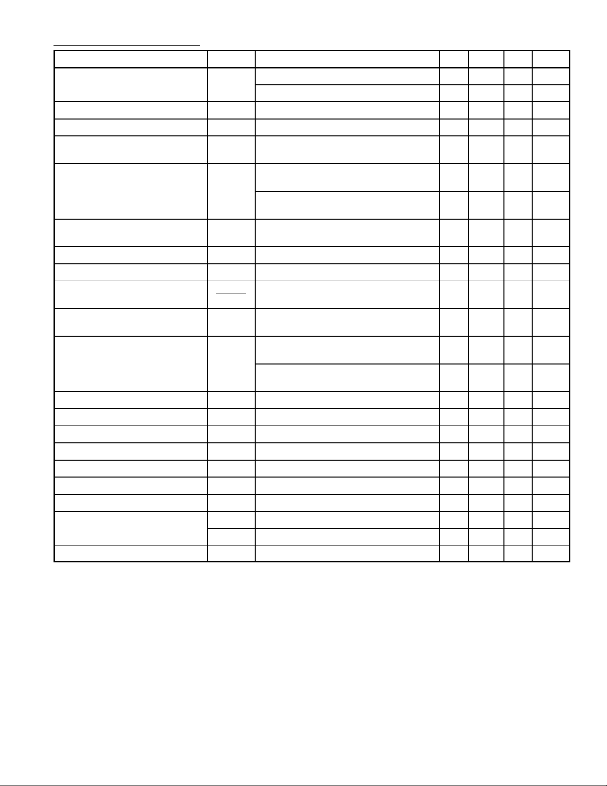
Electrical Characteristics: (VCC = 12V, TA = +25°C unless otherwise specified)
Parameter Symbol Test Conditions Min Typ Max Unit
Supply Current I
CC
R5 = ∞ 10 14 18 mA
R5 = 0 11 – 20 mA
IF Voltage Gain G
IF Output Voltage (Each Output) V
AF Output Voltage V
AF
f = 5.5MHz – 68 – dB
V
At Limiting 170 250 – mV
O
f = 5.5MHz, ∆f = ±50kHz,f
V
= 10mV, Q = 45
I
Distortion f = 5.5MHz, ∆f = 25khz, f
V
= 10mV, Q = 45
I
f = 10.7MHz, ∆f = ±50kHz,f
= 10mV, Q = 20
V
I
Input Voltage Before Limiting V
LIM
f = 5.5MHz, ∆f = ±50kHz,f
Q = 45
Input Impedance Z
Output Resistance R
f = 5.5MHz 15/6 40/4.5 – kΩ/pF
I
O
Volume Control Range Vaf Max
V
Min
af
DC Component of the Output
V
VI = 0 6.2 7.3 8.4 V
8
Signal
AM Rejection a
AM
f = 5.5MHZ, ∆f = ±50kHZ, f
= 500µV, MOD = 30%
V
I
f = 5.5MHZ, ∆f = ±50HZ, f
= 10mV, MOD = 30%
V
I
Potentiometer Resistance R
Potentiometer Voltage V
Potentiometer Resistance R
Potentiometer Voltage V
Noise Voltage at Output V
Zener Voltage V
Zener Slope Resistance R
Breakdown Voltage V
(BR)CBO
V
(BR)CEOI3
Current Gain h
FE
1dB Attenuation – 3.7 4.7 kΩ
5
1dB Attenuation – 2.2 2.5 V
5
70dB Attenuation 1.0 1.4 – kΩ
5
70dB Attenuation – 1.2 – V
5
VI = 10mV – 30 – µV
5
I12 = 5mA 11.2 12.0 13.4 V
12
Z
= 500µA 18 24 – V
I3 = 1mA 50 100 500
MOD
MOD
MOD
MOD
MOD
MOD
= 1kHz,
= 1kHz,
= 1kHz,
= 1kHz,
= 1kHZ,
= 1kHZ,
P–P
0.7 1.0 – V
– 1.5 – %
– 0.2 – %
– 30 60 µV
1.9 2.6 3.3 kΩ
70 85 – dB
50 60 – dB
– 68 – dB
– 30 50 Ω
45 65 – V
 Loading...