

NTE NTE1285, NTE1286 Datasheet

NTE1285 & NTE1286
Integrated Circuit
Audio Power Amplifier, 5.8W
Description:
The NTE1285 and NTE1286 are audio power amplifiers in a 7–Lead SIP type package designed especially for car radio and car stereo applications. These devices are encapsulated in newly developed
small packages featuring low thermal resistance, providing easy design for 2Ω. At 14.4V the devices
give output power of 7W with RL = 4Ω and 11W with RL = 2Ω.
Features:
D High Output Power
D Low Transient Noise at Power Supplu Switch ON
D Mirror Image Pin Configurations
D Protection Circuits are Provided for the Following:
Load Dump Protection
Thermal Shut–Down Protection
Overvoltage Protection
Output Terminal Short–Circuit Protection
Absolute Maximum Ratings: (TA = +25°C unless otherwise specified)
Supply Voltage (Surge PW = 200ms), VCCsurge 40V. . . . . . . . . . . . . . . . . . . . . . . . . . . . . . . . . . . . . . . .
Supply Voltage (Quiescent, Note 1), VCC1 25V. . . . . . . . . . . . . . . . . . . . . . . . . . . . . . . . . . . . . . . . . . . . .
Supply Voltage (Operational), VCC2 18V. . . . . . . . . . . . . . . . . . . . . . . . . . . . . . . . . . . . . . . . . . . . . . . . . .
Peak Circuit Current, ICCpeak 4.5A. . . . . . . . . . . . . . . . . . . . . . . . . . . . . . . . . . . . . . . . . . . . . . . . . . . . . . .
Packag Dissipation, P
Operating Temperature Range (Note 1), T
Storage Temperature Range, T
D
opr
stg
–30° to +75°C. . . . . . . . . . . . . . . . . . . . . . . . . . . . . . . . . .
–55° to +150°C. . . . . . . . . . . . . . . . . . . . . . . . . . . . . . . . . . . . . . . . . .
Note 1. Using an aluminum heat sink 100mm x 100mm x 1mm.
Recommended Operating Conditions: (TA = +25°C unless otherwise specified)
Supply Voltage Range, V
Load Impedance, R
L
CC
9.5V to 16V. . . . . . . . . . . . . . . . . . . . . . . . . . . . . . . . . . . . . . . . . . . . . . . . . .
4Ω to 2Ω. . . . . . . . . . . . . . . . . . . . . . . . . . . . . . . . . . . . . . . . . . . . . . . . . . . . . . . . . . .
12W. . . . . . . . . . . . . . . . . . . . . . . . . . . . . . . . . . . . . . . . . . . . . . . . . . . . . . . . . . . .
Electrical Characteristics: (TA = +25°C, f = 1kHz, RL = 4Ω unless otherwise specified)
Parameter Symbol Test Conditions Min Typ Max Unit
Circuit Current I
Output Power P
CC
u
= 0, VCC = 13.2V 23 45 80 mA
in
RL = 4Ω, THD = 10%, VCC = 13.2V 5.0 5.8 – W
O
RL = 4Ω, THD = 10%, VCC = 14.4V – 7.0 – W
RL = 2Ω, THD = 10%, VCC = 13.2V – 9.2 – W
RL = 2Ω, THD = 10%, VCC = 14.4V – 11.0 – W
Total Harmonic Distortion THD PO = 0.5W – 0.3 1.0 %
Voltage Gain Au PO = 0.5W 51.0 53.5 56.0 dB
Output Noise Level u
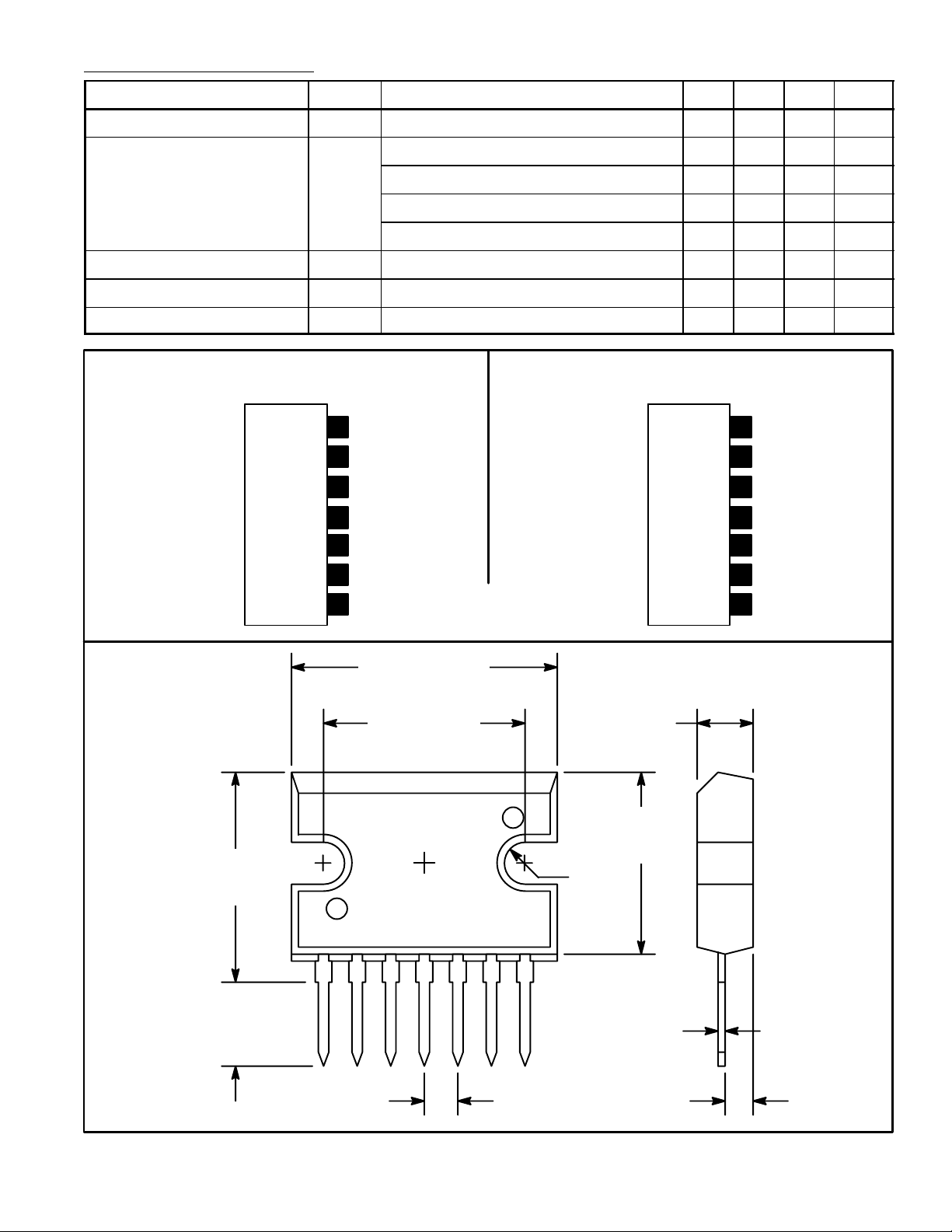
Pin Connection Diagram
(Front View)
7
6
5
NTE1285 NTE1286
4
3
Rg = 10kΩ – 1.4 4.0 mV
n
Pin Connection Diagram
(Front View)
Input
V
CC
Bootstrap
Output
GND
Feedback
7
Bypass
6
Feedback
5
GND
4
Output
3
rms
.590
(15.0)
Max
.256
(6.5)
Bypass
2
1
Input
.787 (20.0) Max
.590 (15.0)
Max
17
.158 (4.0)
Max
.512
(13.0)
Max
.071
(1.8)
R
.010 (.254)
Bootstrap
2
1
V
CC
.100 (2.45)
.083 (2.1)
 Loading...