

NTE NTE1254 Datasheet

NTE1254
Integrated Circuit
Phase–Lock Loop (PLL) Frequency
Synthesizer for CB
Features:
D Programmable Divider – Divided by 3 to 255
D 10–Bit Divider
D Phase Detector
D Reference Oscillation Circuit
D On–Chip Filter Amplifier
D Code Converter
D Only two or three crystals required for CB radio AM frequency selection
D Unlocked signals are detected at instant stop “IS” terminal
D Two type program mode can be selected to change input mode level
M: Low level Binary code input enables, divided by 3 to 255.
M: High level BCD code enables that the data at P
D Internal active filter amplifier has a long holding time due to very high input impedance charac-
teristics of the CMOS–this is to obtain very good spurious response.
D Output signal of the “I” can be used to stop the spurious radiation when the channel selector
makes misprogramming such as rotary switch’s lose contact.
D High speed and low power consumption due to CMOS
D Single power supply and fully TTL compatible: V
D Operating Temperature: T
D Pull down resistors installed in program and mode switch inputs
= –30° to 65°C
A
DD
to P6 port is offset 90 by code converter.
1
= 5 ± 0.5 Volts
Absolute Maximum Ratings:
Supply Voltage –0.3 to +6.0V. . . . . . . . . . . . . . . . . . . . . . . . . . . . . . . . . . . . . . . . . . . . . . . . . . . . . . . . . . . .
Input Voltage –0.3 to +6.0V. . . . . . . . . . . . . . . . . . . . . . . . . . . . . . . . . . . . . . . . . . . . . . . . . . . . . . . . . . . . .
Operating Temperature Range, T
Storage Temperature Range, T
opr
stg
–35° to +75°C. . . . . . . . . . . . . . . . . . . . . . . . . . . . . . . . . . . . . . . . .
–55° to +125°C. . . . . . . . . . . . . . . . . . . . . . . . . . . . . . . . . . . . . . . . . .
Electrical Characteristics: (TA = – 35° to +75°C unless otherwise specified)
Parameter Symbol Test Conditions Min Typ Max Unit
Power Supply V
Total Current I
High Level Input Voltage V
Low Level Input Voltage V
High Level Output Voltage V
Low Level Output Voltage V
Leakage Current I
Input Capacitance C
Maximum Frequency
Response
fdmax X1 – X2, Divider 11 – – MHz
fpmax Programmable Divider – 2 – MHz
DD
f = 0 – – 10 mA
DD
All Inputs 0.8V
IH
All Inputs –0.3 – 0.2V
IL
All Outputs Except D2, IO = –0.3mA,
OH
V
= 4.5V
DD
IO = –0.15mA, VDD = 4.5V 0.85V
All Inputs, IO = 0.5mA, VDD = 4.5V –0.3 – 0.15V
OL
EO (Floating), Al TA = +25°C – 1.0 – nA
L
PI, FD, FP, X1, Vi = 0 – – 10 pF
i
4.5 5.0 5.5 V
DD
DD
– V
– V
– V
DD
0.85V
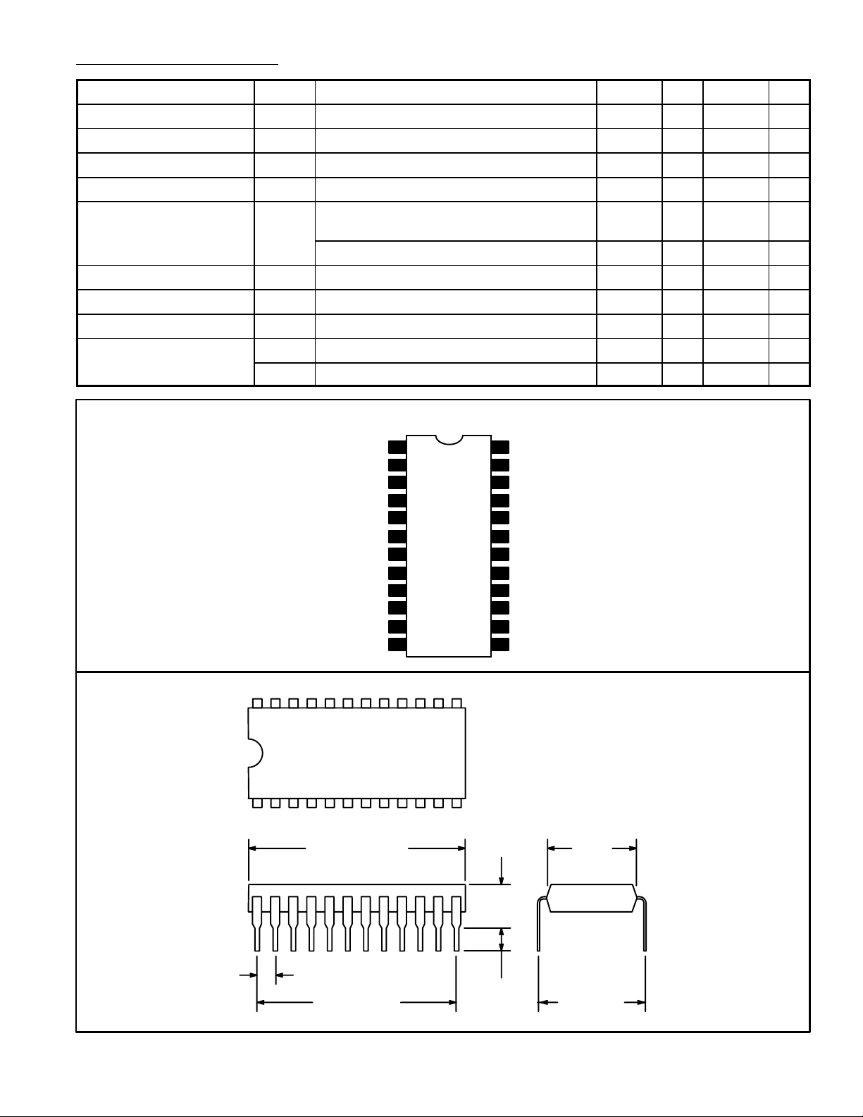
Pin Connection Diagram
Program Input P1
Program Input P2
Program Input P3
Program Input P4
Program Input P6
X’tal Input
X’tal Input
V
DD
1
2
3
4
5Program Input P5
6
7Program Input P7
8Program Input P8
91/2 Output Reference
10
11
12
24
Inhibit Output
23
V
SS
22
Instant Stop
21
Phase Error Output
20
Filter Amp Input
19
Filter Amp Output
Detector Input
18
17
Divider Output
Detector Input
16
Divider Output
15
14
Input Mode Switch
Divider Input
13
DD
DD
DD
DD
DD
V
V
V
V
V
24 13
112
1.300 (33.02)
.100 (2.54)
1.100 (27.94)
Max
.225
(5.73)
Max
.126
(3.22)
Min
.520
(13.2)
.600
(15.24)
 Loading...