

NTE NTE1199 Datasheet

NTE1199
Integrated Circuit
CMOS Frequency Divider
Description:
The NTE1199 is an LSI CMOS circuit in a 24–Lead DIP type package designed for use in frequency
divider applications in CB transceivers. This device contains a prescaler, divider, and binary input
programmable circuitry.
Absolute Maximum Ratings:
Supply Voltage, V
Input Voltage, V
Output Voltage, V
Output Current, I
DD
I
O
O
(TA = +25°C unless otherwise specified)
Pins 17, 21, 22, 24 ±5mA. . . . . . . . . . . . . . . . . . . . . . . . . . . . . . . . . . . . . . . . . . . . . . . . . . . . . . . . .
Pins 13, 19 ±10mA. . . . . . . . . . . . . . . . . . . . . . . . . . . . . . . . . . . . . . . . . . . . . . . . . . . . . . . . . . . . . . .
Operating Temperature Range, T
Storage Temperature Range, T
Electrical Characteristics:
Parameter Symbol Test Conditions Min Typ Max Unit
Input Voltage
High Level
Low Level V
Output Voltage (Pins 17, 21, 22, 24)
High Level
Low Level V
Output Voltage (Pins 13, 19)
High Level
Low Level V
Total Current I
Count Pulse Rise Time t
Count Pulse Fall Time t
Input Capacitance (Pins 14, 16, 18) C
Frequency Response f
opr
stg
(VDD = +5V, TA = –30° to +60°C unless otherwise specified)
–0.3 to +6.0V. . . . . . . . . . . . . . . . . . . . . . . . . . . . . . . . . . . . . . . . . . . . . . . . . . . . . . .
–0.3 to +6.0V. . . . . . . . . . . . . . . . . . . . . . . . . . . . . . . . . . . . . . . . . . . . . . . . . . . . . . . . . .
–0.3 to +6.0V. . . . . . . . . . . . . . . . . . . . . . . . . . . . . . . . . . . . . . . . . . . . . . . . . . . . . . . .
–30° to +60°C. . . . . . . . . . . . . . . . . . . . . . . . . . . . . . . . . . . . . . . . .
–55° to +125°C. . . . . . . . . . . . . . . . . . . . . . . . . . . . . . . . . . . . . . . . . .
V
V
OH
V
OH
DD
f
f
All Inputs
IH
All Inputs –0.3 – 1.25 V
IL
IO = –300µA
IO = 300µA –0.3 – 0.4 V
OL
IO = –4.8mA
IO = 4.8mA –0.3 – 0.4 V
OL
f = 0 – 10 – mA
See Pulse Definition (Fig. 1) – – 5 µs
r
f
VI = 0 – – 10 pF
I
Prescaler 10 – – MHz
s
Divider 7 – – MHz
d
Programmable Divider
p
(Apply Program Table, Fig. 2)
4.0 – +V
2.4 – +V
2.4 – +V
– – 5 µs
5 – – MHz
DD
DD
DD
V
V
V
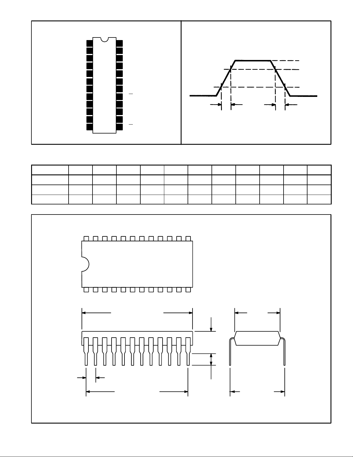
Fig. 1 Pulse DefinitionPin Connection Diagram
P
1
1
P
2
2
3
P
3
P
4
4
5
P
5
6
P
6
7
P
7
P
8
8
P
9 16
9
P
10
10
11
P
11
12 13
V
DD
D
24
6
23
GND
22
D
7
D
21
8
20
M
19 DO
18
DI
SO
17
SI
C
15
14
PI
PO
V
IH
VIH (Min)
(Min)
V
IL
t
r
t
f
Fig. 2 Program Table
P
1
P
2
P
3
P
4
P
5
P
6
P
7
P
8
P
9
P
10
P
Pat. 1 1 0 0 1 1 0 0 1 1 1 1
Pat. 2 0 1 1 0 0 1 1 0 0 0 0
Pat. 3 1 1 0 0 0 0 0 0 0 0 0
V
IL
11
24 13
112
1.300 (33.02)
Max
.520
(13.2)
.225
(5.73)
Max
.100 (2.54)
.126
1.100 (27.94)
(3.22)
Min
.600
(15.24)
 Loading...