

NTE NTE1172 Datasheet
NTE1172
Integrated Circuit
Phase–Frequency Detector
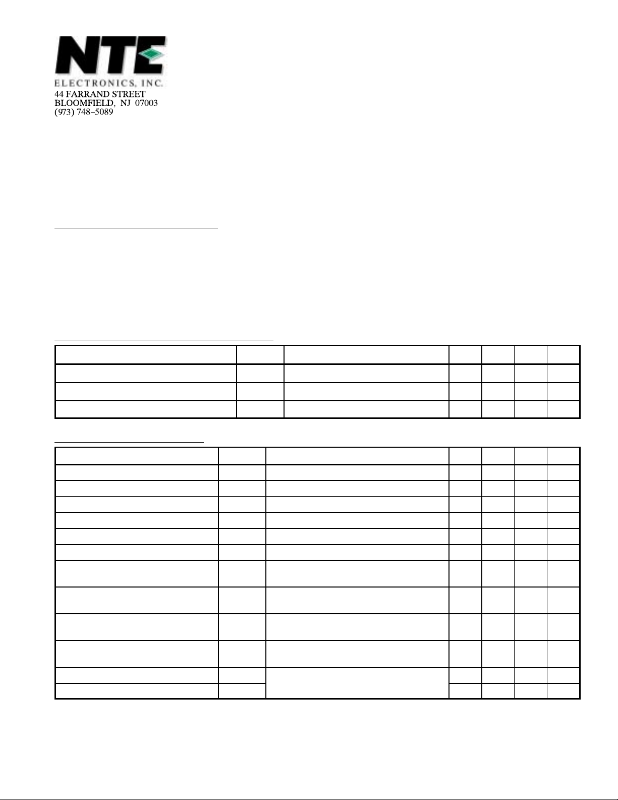
Absolute Maximum Ratings: (TA = +25°C unles otherwise specified)
Supply Voltage, V
Input Voltage, V
Output Voltage, V
Power Dissipation, P
Operating Temperature Range, T
Storage Temperature Range, T
Recommended Operating Conditions:
Parameter Symbol Test Conditions Min Typ Max Unit
CC
I
O
D
opr
stg
7V. . . . . . . . . . . . . . . . . . . . . . . . . . . . . . . . . . . . . . . . . . . . . . . . . . . . . . . . . . . . . . . . .
5.5V. . . . . . . . . . . . . . . . . . . . . . . . . . . . . . . . . . . . . . . . . . . . . . . . . . . . . . . . . . . . . . . . . .
5.5V. . . . . . . . . . . . . . . . . . . . . . . . . . . . . . . . . . . . . . . . . . . . . . . . . . . . . . . . . . . . . . . .
360mW. . . . . . . . . . . . . . . . . . . . . . . . . . . . . . . . . . . . . . . . . . . . . . . . . . . . . . . . . .
–15° to +75°C. . . . . . . . . . . . . . . . . . . . . . . . . . . . . . . . . . . . . . . . .
–40° to +125°C. . . . . . . . . . . . . . . . . . . . . . . . . . . . . . . . . . . . . . . . . .
Supply Voltage V
Input Voltage, High Level V
Input Voltage, Low Level V
CC
IH
IL
4.75 5.0 5.25 V
2.0 – 5.0 V
0 – 0.8 V
Electrical Charactersitics: (TA = –15° to +75°C, GND = Pin7, Note 1 unless otherwsie specified)
Parameter Symbol Test Conditions Min Typ Max Unit
Low Level Input Current (Pin1) I
Low Level Input Current (Pin3) I
Low Level Input Current (Pin11) I
High Level Input Current (Pin1) I
High Level Input Current (Pin3) I
High Level Input Current (Pin11) I
Low Level Output Voltage (Pin6) V
Low Level Output Voltage (Pin12) V
High Level Output Voltage (Pin6) V
High Level Output Voltage (Pin12) V
High Level Output Voltage (Pin2) V
Low Level Output Voltage (Pin13) V
IH
IH
IH
OL
OL
OH
OH
OH
OL
IL
IL
IL
VCC = 5.25V, V
VCC = 5.25V, V
VCC = 5.25V, V
VCC = 5.25V, V
VCC = 5.25V, V
VCC = 5.25V, V
VCC = 4.75V, V
I
= 20mA
OL(6)
VCC = 4.75V, V
= 20mA
I
OL(12)
VCC = 4.75V, V
I
= –1.6mA
OH(6)
VCC = 4.75V, V
I
= –1.6mA
OH(12)
VCC = 4.75V, V
I
= –1.6mA, I
OH(2)
= 0.4V – – –4.8 mA
IL(1)
= 0.4V – – –4.8 mA
IL(3)
= 0.4V – – –1.6 mA
IL(11)
= 2.5V – – 120 µA
IH(1)
= 2.5V – – 120 µA
IH(3)
= 2.5V – – 40 µA
IH(11)
IH(1,3)
IH(1,3)
IH(1,3)
IH(1,3)
OL(1,3)
OL(13)
= 1.8V,
= 1.2V,
= 1.8V,
= 1.8V,
= 1.1V,
= 20mA, Note 2
– – 0.4 V
– – 0.4 V
2.5 – – V
2.5 – – V
2.5 – – V
– – 0.4 V
Note 1. Pin numbers shown in ( ).
Note 2. This value is measured at Input State 9 of the truth table and varies depending on the situa-
tion of sequential logic.
Electrical Charactersitics:
(TA = –15° to +75°C GND = Pin7, Note 1 unless otherwsie specified)
Parameter Symbol Test Conditions Min Typ Max Unit
High Level Output Voltage (Pin2) V
Low Level Output Voltage (Pin13) V
Short Circuit Output Current (Pin2) I
Short Circuit Output Current (Pin6) I
Short Circuit Output Current (Pin12) I
Short Circuit Output Current (Pin13) I
Output Voltage (Pin10) V
Output Current (Pin8) I
Output Leakage Current (Pin2) I
OH
OL
OS
OS
OS
OS
EH
O
OLK
VCC = 4.75V, V
I
= –0mA, I
OH(2)
V
= 1.8V, GND (2, 3, 7) –20 – –65 mA
IH(1)
= 1.1V,
OL(1,3)
= –1.6mA, Note 3
OL(13)
VCC = 5V, GND (1, 3, 6, 7) –20 – –65 mA
VCC = 5V, GND (1, 3, 7 ,12) –20 – –65 mA
VCC = 5V, V
I
= –1mA, V
OH(10)
V
= 5.25V, I
CC(8)
V
CC (2,14)
= 1.8V, GND (3, 7, 13) –20 – –65 mA
IH(1)
= 1.1V 1.5 – – V
IL(11)
= 2µA 0.8 – – mA
A(9)
= 5V, V
IH(1)
= 1.8V,
2.5 – – V
– – 0.4 V
– – 250 µA
GND (3, 7)
Output Leakage Current (Pin6) I
Output Leakage Current (Pin12) I
Output Leakage Current (Pin13) I
OLK
OLK
OLK
V
CC (6,14)
V
CC (12,14)
V
CC (2,14)
= 5V, GND (1, 3, 9) – – 250 µA
= 5V, GND (1, 3, 7) – – 250 µA
= 5V, V
IH(1)
= 1.8V,
– – 250 µA
GND (3, 7)
Collector–Emitter Voltage V
Output Leakage Current (Pin8) I
Output Leakage Current (Pin10) I
Supply Current I
CE
OLK
OLK
CC
I
= 1mA, GND (4, 7) 0.5 – – V
in(15)
V
= 5.25V, GND (7, 9) – – 120 µA
CC(8)
VCC = 5.25V, V
= 1.5V
V
O(10)
IH(11)
= 2.5V,
– – 5 µA
VCC = 5V – – 40 mA
Switching Characteristics
Maximum Count Pulse Frequency f
Propagation Delay Time t
max1
f
max2
PHL1
t
PLH1
t
PHL2
t
PLH2
CL = 15pF, RL = 300Ω – 30 – MHz
– 30 – MHz
– 13 – ns
– 19 – ns
– 4.5 – ns
– 10 – ns
Note 1. Pin numbers shown in ( ).
Note 2. This value is measured at Input State 13 of the truth table and varies depending on the situa-
tion of sequential logic.
Truth Table:
Input
Input
State
Ref Variable Upper 1 Down 1 Upper 2 Down2
1 0 0 X X 1 1
2 1 0 X X 0 1
3 1 1 X X 1 0
4 1 0 X X 0 1
5 0 0 X X 1 1
6 1 0 X X 0 1
7 0 0 X X 1 1
8 1 0 X X 0 1
9 0 0 0 1 1 1
10 0 1 0 1 1 1
11 0 0 1 1 1 1
12 0 1 1 1 1 1
13 0 0 1 0 1 1
14 0 1 1 0 1 1
15 0 0 1 0 1 1
16 1 0 1 0 0 1
17 0 0 1 1 1 1
(0 = L, 1 = H, X = Don’t Care)
Input Output
Pin Connection Diagram
Reference
Down 1
Variable
Charge Pump Upper
Down 2
GND
1
2
3
4
5
6
7
V
14
CC
13
Upper 1
12
Upper 2
11
Charge Pump DownCharge Pump Upper
10
Charge Pump Down
Filter Amp
9
8
Filter Amp
 Loading...