

NTE NTE1115A, NTE1115 Datasheet
NTE1115 & NTE1115A
Integrated Circuit
Audio Power Amplifier, 7W
Description:
The NTE1115 and NTE1115A are monolithic integrated circuits designed for use as low frequency
class B amplifiers. These devices provide 7W power output at 16V/4Ω, 6W at 14.4V/4Ω, 2.5W at
9V/Ω, 1W at 6V/4Ω and works with a wide range of supply voltages (4V to 20V); and gives high output
current (up to 2.5A), high efficiency (75% at 6W output), very low harmonic and cross–over distortion.
In addition, thermal protection is provided.
Absolute Maximum Ratings:
Supply Voltage, V
Output Peak Current (Non–Repetitive), I
Output Current (Repetitive), I
Power Dissipation, P
S
O
O
tot
TA = +70°C 1W. . . . . . . . . . . . . . . . . . . . . . . . . . . . . . . . . . . . . . . . . . . . . . . . . . . . . . . . . . . . . . . . . .
T
= +100°C 5W. . . . . . . . . . . . . . . . . . . . . . . . . . . . . . . . . . . . . . . . . . . . . . . . . . . . . . . . . . . . . . . .
tab
Operating Junction Temperature Range, T
Storage Temperature Range, T
stg
Thermal Resistance, Junction–to–Tab, R
J
thJ–TAB
NTE1115 10°C/W. . . . . . . . . . . . . . . . . . . . . . . . . . . . . . . . . . . . . . . . . . . . . . . . . . . . . . . . . . . . . . . .
NTE1115A 12°C/W. . . . . . . . . . . . . . . . . . . . . . . . . . . . . . . . . . . . . . . . . . . . . . . . . . . . . . . . . . . . . . .
Thermal Resistance, Junction–to–Ambient, R
NTE1115 80°C/W. . . . . . . . . . . . . . . . . . . . . . . . . . . . . . . . . . . . . . . . . . . . . . . . . . . . . . . . . . . . . . . .
NTE1115A (Note 1) 70°C/W. . . . . . . . . . . . . . . . . . . . . . . . . . . . . . . . . . . . . . . . . . . . . . . . . . . . . . .
–40° to +150°C. . . . . . . . . . . . . . . . . . . . . . . . . . . . . . . . . .
–40° to +150°C. . . . . . . . . . . . . . . . . . . . . . . . . . . . . . . . . . . . . . . . . .
thJA
20V. . . . . . . . . . . . . . . . . . . . . . . . . . . . . . . . . . . . . . . . . . . . . . . . . . . . . . . . . . . . . . . . .
3.5A. . . . . . . . . . . . . . . . . . . . . . . . . . . . . . . . . . . . . . . . . . . .
2.5A. . . . . . . . . . . . . . . . . . . . . . . . . . . . . . . . . . . . . . . . . . . . . . . . . . . . . .
Note 1. Obtained with tabs soldered to printed circuit with minimized copper area.
Elecrtrical Characteristics:
Parameter Symbol Test Conditions Min Typ Max Unit
Supply Voltage (Pin1) V
Quiescent Output Voltage (Pin12) V
Quiescent Drain Current I
Bias Current (Pin8) I
(TA = +25°C unless otherwise specified)
S
VS = 14.4V 6.4 7.2 8.0 V
O
d
b
4 – 20 V
– 12 20 mA
– 0.4 – µA
Elecrtrical Characteristics (Cont’d): (TA = +25°C unless otherwise specified)
Parameter Symbol Test Conditions Min Typ Max Unit
Power Output P
Input Voltage V
Input Sensitivity V
Input Resistance (Pin8) R
Frequency Response (–3dB) B VS = 14.4V, RL = 4Ω C3 = 820pF 40 to 20,000 Hz
Total Harmonic Distortion THD PO = 50mW to 3W, VS = 14.4V, RL = 4Ω,
Voltage Gain (Open Loop) G
Voltage Gain (Closed Loop) G
Input Noise Voltage e
Input Noise Current i
Efficiency h PO = 5W, VS = 14.4V, RL = 4Ω, f = 1kHz – 70 – %
i(rms)
THD = 10%, RL = 4Ω,
O
f = 1kHz
PO = 6W, VS = 14.4V,
i
RL = 4Ω, f = 1kHz
i
f = 1kHz
VS = 14.4V, RL = 4Ω, f = 1kHz – 80 – dB
V
V
VS = 14.4V, Rg = 0,
N
B (–3dB) = 20Hz to 20kHz
VS = 14.4V, B (–3dB) = 20Hz to 20kHz – 0.1 – nA
N
VS = 16V – 7.0 – W
VS = 14.4V 5.5 6.0 – W
VS = 9V – 2.5 – W
VS = 6V – 1.0 – W
– – 22 mW
Rf = 56Ω – 80 – mV
Rf = 22Ω – 35 – mV
– 5 – MΩ
C3 = 1500pF 40 to 10,000 Hz
– 0.3 – %
34 37 40 dB
– 2 – µV
Supply Voltage Rejection SVR VS = 14.4V, RL = 4Ω, f
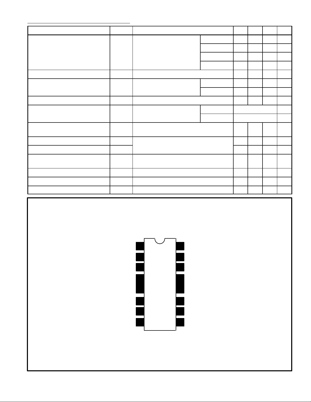
Pin Connection Diagram
V
CC
N.C.12
N.C.
3
12
11
10
Tab
Tab
Bootstrap
Compensation
Feedback
4
5
6
9
8
7
= 100Hz – 38 – dB
ripple
Output
N.C.
GND
Substrate GND
Input
Ripple Rejection
 Loading...