

Page 1

NTE7242
Integrated Circuit 12 Watt Low Power
Off Line SMPS Primary Switcher
8−Lead DIP
Description:
The NTE7242 combines a dedicated current mode PWM controller with a high voltage Power MOSFET
on the same silicon chip. Typical applications cover off line power supplies for battery charger adapters,
standby power supplies for TV or monitors, auxiliary supplies for motor control, etc. The internal control
circuit offers the following benefits:
D Large input voltage range on the V
This feature is well adapted to battery charger adapter configurations.
D Automatic burst mode in low load condition.
D Overvoltage protection in hiccup mode.
Features:
D Fixed 60 KHZ Switching Frequency
D 9V to 38V Wide Range V
Voltage
DD
D Current Mode Control
D Auxiliary Undervoltage Lockout with Hysteresis
D High Voltage Start Up Current Source
D Overtemperature, Overcurrent and Overvoltage Protection with Autorestart
pin accommodates changes in auxiliary supply voltage.
DD
Absolute Maximum Ratings:
Supply Voltage, V
Switching Drain Source Voltage (T
Start Up Drain Source Voltage (T
Continuous Drain Current, I
Feedback Current, I
Operating Junction Temperature Range, T
Case Operating Temperature Range, T
Storage Temperature Range, T
Thermal Resistance, Junction−to−Case, R
DD
FB
= +25 to +125°C, Note 1), V
J
= +25 to +125°C, Note 2), V
J
D
J
C
stg
thJC
Thermal Resistance, Junction−to−Ambient (Note 3), R
Electrostatic Discharge, V
Machine Model (R=0W; C=200pF)
(ESD
)
thJA
DS(sw)
DS(st)
−0.3 to 730V............
−0.3 to 400V..............
Internally limited.............................................
Internally limited.................................
−40 to +150°C....................................
−55 to +150°C..........................................
50V................................................................
3mA.............................................................
+15°C/W....................................
+45°C/W..........................
200V............................................
Charged Device Model 1.5kV......................................................
Note 1. This parameter applies when the start up current source is off. This is the case when the V
voltage has reached V
and remains above V
DDon
DDoff
.
Note 2. This parameter applies when the start up current source is on. This is the case when the V
voltage has not yet reached V
Note 3. When mounted on a standard single−sided FR4 board with 200mm
or has fallen below V
DDon
DDoff
.
2
of Cu (at least 35mm thick)
connected to all DRAIN pins.
DD
DD
Page 2
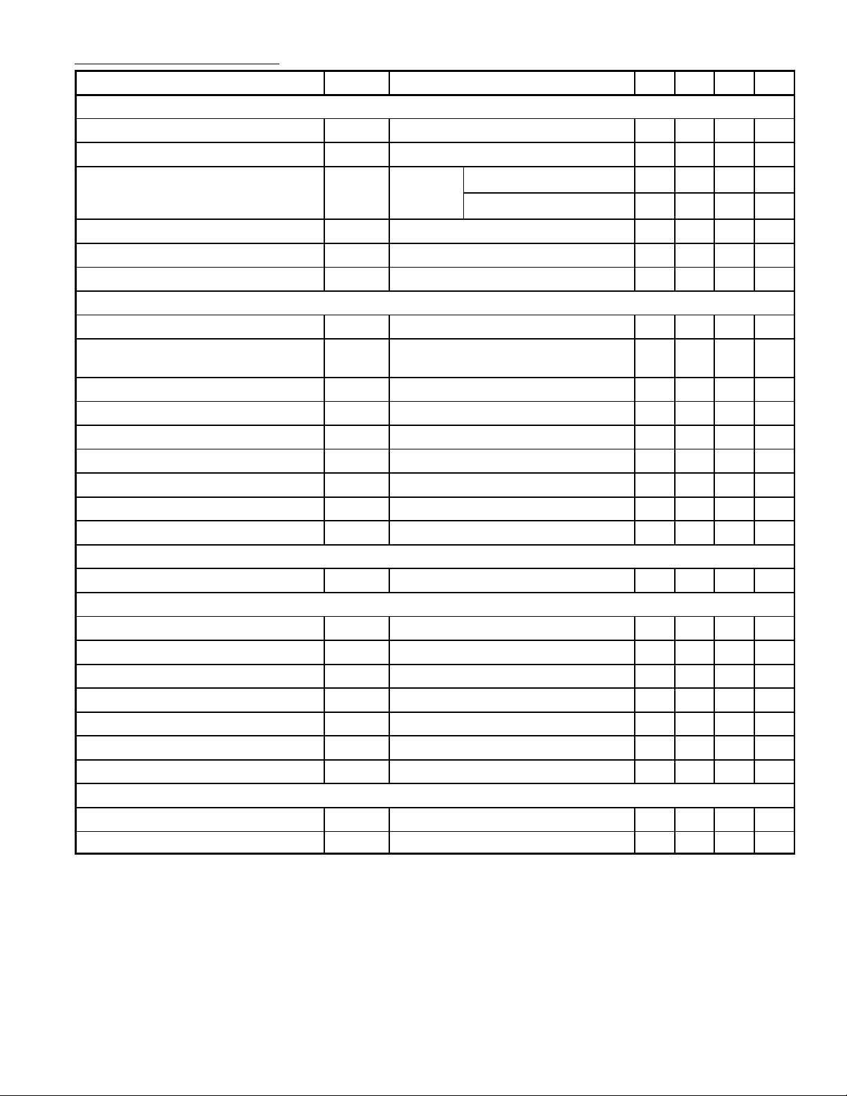
Electrical Characteristics: (TJ=+25°C, VDD=18V, unless otherwise specified)
Parameter Symbol Test Conditions Min Typ Max Unit
Power
Drain−Source Voltage BV
Off State Drain Current I
Static Drain−Source On State
R
Resistance
Fall Time t
Rise Time t
Drain Capacitance C
Supply
Start Up Charging Current I
Start Up Charging Current in Thermal
DDch
I
DDoff
Shutdown
Operating Supply Current Not Switching I
Operating Supply Current Switching I
Restart Duty Cycle D
VDD Undervoltage Shutdown Threshold V
VDD Start Up Threshold V
VDD Threshold Hysteresis V
VDD Overvoltage Hysteresis V
DDhyst
DDovp
Oscillator
DSSID
DSS
DSonID
VDS=500V, VFB=2V, TJ=+125°C − − 0.1 mA
ID=0.2A, VIN=300V, Note 4 − 100 − ns
f
ID=0.4A, VIN=300V, Note 4 − 50 − ns
r
VDS=25V − 40 − pF
oss
VDS=100V, VDD=0V to V
VDD=5V, VDS=100V, TJ > TSD − T
DD0
DD1
RST
DDoff
DDon
IFB=2mA − 3 5 mA
IFB=0.5mA, ID=50mA, Note 5 − 4.5 − mA
=1mA, VFB=2V 730 − − V
=0.4A − 15 17
TJ=+100°C − − 31
DDon
HYST
− −1 − mA
0 − − mA
W
W
− 16 − %
7 8 9 V
13 14.5 16 V
5.8 6.5 7.2 V
38 42 46 V
Oscillator Frequency Total Variation F
OSC
VDD=V
to 35V, TJ=0 to +100°C 54 60 66 kHz
DDoff
PWM Comparator
IFB to ID Current Gain G
Peak Current Limitation I
IFB Shutdown Current I
FB Pin Input Impedance R
Current Sense Delay to Turn−Off t
Blanking Time t
Minimum Turn On Time t
ONmin
ID
Dlim
FBsd
FB
d
b
VFB=0V 0.56 0.7 0.84 A
ID=0mA
ID=0.4A − 200 − ns
− 560 − −
− 0.9 − mA
− 1.2 −
kW
− 500 − ns
− 700 − ns
Overtemperature
Thermal Shutdown Temperature T
Thermal Shutdown Hysteresis T
SD
HYST
140 170
− 40
°C
−
°C
−
Note 4. On clamped inductive load.
Note 5. These test conditions obtained with a resistive load are leading to the maximum conduction
time of the device.
Page 3

Pin Connection Diagram
Source
Source
VDD Drain
FB
1
2
3
4
85
.280 (7.1)
Drain
8
7
Drain
6
Drain
5
14
.400 (10.16)
Max
.200
(5.08)
.100 (2.54)
.300
(7.62)
.125 (3.17) Min
07/26/2016
 Loading...