NSC MM54C04J-883, MM54C04W-883 Datasheet

TL/F/5877
MM54C00/MM74C00, MM54C02/MM74C02, MM54C04/MM74C04,
MM54C10/MM74C10, MM54C20/MM74C20
February 1988
MM54C00/MM74C00 Quad 2-Input NAND Gate
MM54C02/MM74C02 Quad 2-Input NOR Gate
MM54C04/MM74C04 Hex Inverter
MM54C10/MM74C10 Triple 3-Input NAND Gate
MM54C20/MM74C20 Dual 4-Input NAND Gate
General Description
These logic gates employ complementary MOS (CMOS) to
achieve wide power supply operating range, low power consumption, high noise immunity and symmetric controlled
rise and fall times. With features such as this the 54C/74C
logic family is close to ideal for use in digital systems. Function and pin out compatibility with series 54/74 devices minimizes design time for those designers already familiar with
the standard 54/74 logic family.
All inputs are protected from damage due to static discharge by diode clamps to V
CC
and GND.
Features
Y
Wide supply voltage range 3V to 15V
Y
Guaranteed noise margin 1V
Y
High noise immunity 0.45 VCC(typ.)
Y
Low power consumption 10 nW/package (typ.)
Y
Low power Fan out of 2
TTL compatibility driving 74L
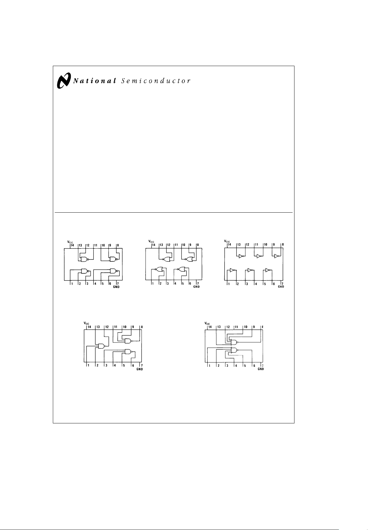
Connection Diagrams
Dual-In-Line Packages
MM54C00/MM74C00
TL/F/5877– 1
Top View
Order Number MM54C00 or
MM74C00
MM54C02/MM74C02
TL/F/5877– 2
Top View
Order Number MM54C02 or
MM74C02
MM54C04/MM74C04
TL/F/5877– 3
Top View
Order Number MM54C04
or MM74C04
MM54C10/MM74C10
TL/F/5877– 4
Top View
Order Number MM54C10 or
MM74C10
MM54C20/MM74C20
TL/F/5877– 5
Top View
Order Number MM54C20 or
MM74C20
C
1995 National Semiconductor Corporation RRD-B30M115/Printed in U. S. A.

Absolute Maximum Ratings
If Military/Aerospace specified devices are required,
please contact the National Semiconductor Sales
Office/Distributors for availability and specifications.
Voltage at Any Pin
b
0.3V to V
CC
a
0.3V
Operating Temperature Range
54C
b
55§Ctoa125§C
74C
b
40§Ctoa85§C
Storage Temperature Range
b
65§Ctoa150§C
Operating V
CC
Range 3.0V to 15V
Maximum VCCVoltage 18V
Power Dissipation (PD)
Dual-In-Line 700 mW
Small Outline 500 mW
Lead Temperature
(Soldering, 10 seconds) 300
§
C
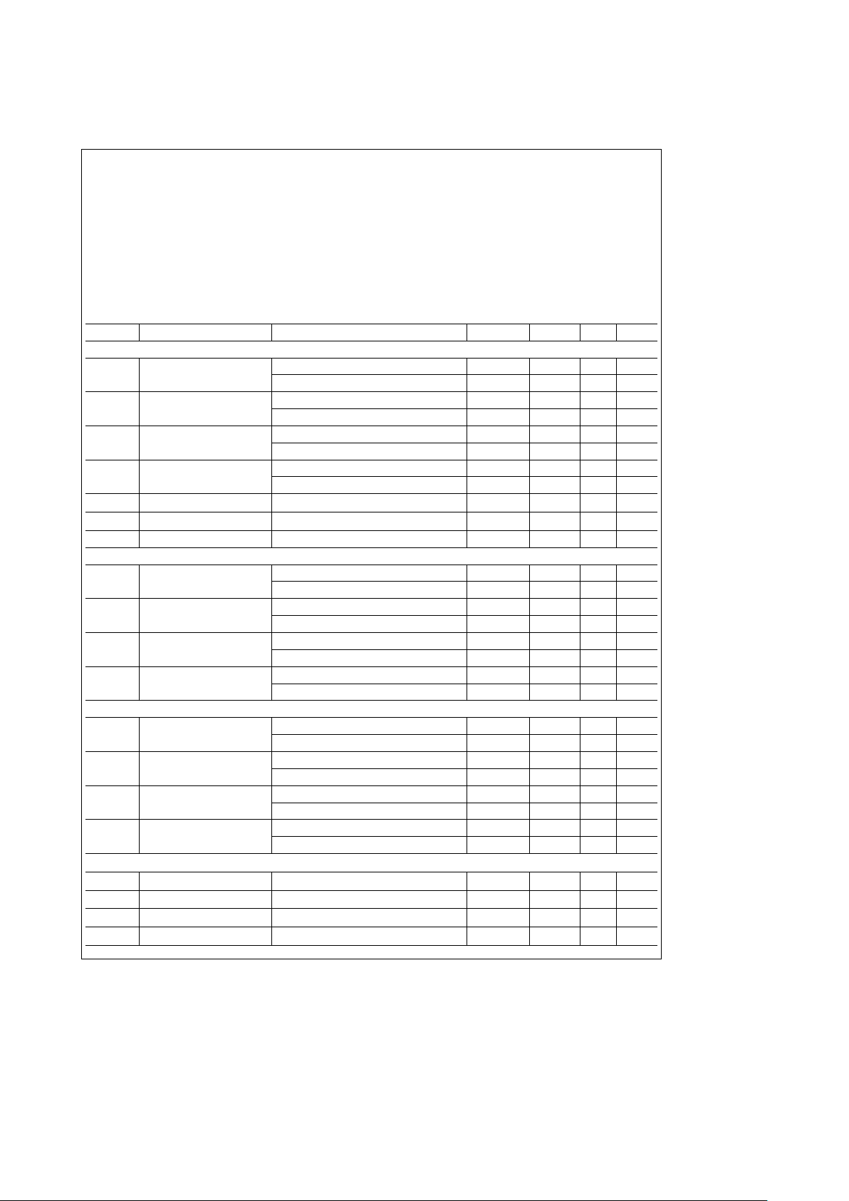
DC Electrical Characteristics
Min/Max limits apply across the guaranteed temperature range unless otherwise noted
Symbol Parameter Conditions Min Typ Max Units
CMOS TO CMOS
V
IN(1)
Logical ‘‘1’’ Input Voltage V
CC
e
5.0V 3.5 V
V
CC
e
10V 8.0 V
V
IN(0)
Logical ‘‘0’’ Input Voltage V
CC
e
5.0V 1.5 V
V
CC
e
10V 2.0 V
V
OUT(1)
Logical ‘‘1’’ Output Voltage V
CC
e
5.0V, I
O
eb
10 mA 4.5 V
V
CC
e
10V, I
O
eb
10 mA 9.0 V
V
OUT(0)
Logical ‘‘0’’ Output Voltage V
CC
e
5.0V, I
O
e
10 mA 0.5 V
V
CC
e
10V, I
O
e
10 mA 1.0 V
I
IN(1)
Logical ‘‘1’’ Input Current V
CC
e
15V, V
IN
e
15V 0.005 1.0 mA
I
IN(0)
Logical ‘‘0’’ Input Current V
CC
e
15V, V
IN
e
0V
b
1.0
b
0.005 mA
I
CC
Supply Current V
CC
e
15V 0.01 15 mA
LOW POWER TO CMOS
V
IN(1)
Logical ‘‘1’’ Input Voltage 54C, V
CC
e
4.5V V
CC
b
1.5 V
74C, V
CC
e
4.75V V
CC
b
1.5 V
V
IN(0)
Logical ‘‘0’’ Input Voltage 54C, V
CC
e
4.5V 0.8 V
74C, V
CC
e
4.75V 0.8 V
V
OUT(1)
Logical ‘‘1’’ Output Voltage 54C, V
CC
e
4.5V, I
O
eb
10 mA 4.4 V
74C, V
CC
e
4.75V, I
O
eb
10 mA 4.4 V
V
OUT(0)
Logical ‘‘0’’ Output Voltage 54C, V
CC
e
4.5V, I
O
e
10 mA 0.4 V
74C, V
CC
e
4.75V, I
O
e
10 mA 0.4 V
CMOS TO LOW POWER
V
IN(1)
Logical ‘‘1’’ Input Voltage 54C, V
CC
e
4.5V 4.0 V
74C, V
CC
e
4.75V 4.0 V
V
IN(0)
Logical ‘‘0’’ Input Voltage 54C, V
CC
e
4.5V 1.0 V
74C, V
CC
e
4.75V 1.0 V
V
OUT(1)
Logical ‘‘1’’ Output Voltage 54C, V
CC
e
4.5V, I
O
eb
360 mA 2.4 V
74C, V
CC
e
4.75V, I
O
eb
360 mA 2.4 V
V
OUT(0)
Logical ‘‘0’’ Output Voltage 54C, V
CC
e
4.5V, I
O
e
360 mA 0.4 V
74C, V
CC
e
4.75V, I
O
e
360 mA 0.4 V
OUTPUT DRIVE (see 54C/74C Family Characteristics Data Sheet) T
A
e
25§C (short circuit current)
I
SOURCE
Output Source Current V
CC
e
5.0V, V
IN(0)
e
0V, V
OUT
e
0V
b
1.75 mA
I
SOURCE
Output Source Current V
CC
e
10V, V
IN(0)
e
0V, V
OUT
e
0V
b
8.0 mA
I
SINK
Output Sink Current V
CC
e
5.0V, V
IN(1)
e
5.0V, V
OUT
e
V
CC
1.75 mA
I
SINK
Output Sink Current V
CC
e
10V, V
IN(1)
e
10V, V
OUT
e
V
CC
8.0 mA
2
 Loading...