NSC MM5452VX, MM5452N, MM5452MDC, MM5452V, MM5452MWC Datasheet

TL/F/6137
MM5452/MM5453 Liquid Crystal Display Drivers
February 1995
MM5452/MM5453 Liquid Crystal Display Drivers
General Description
The MM5452 is a monolithic integrated circuit utilizing
CMOS metal gate, low threshold enhancement mode devices. It is available in a 40-pin molded package. The chip can
drive up to 32 segments of LCD and can be paralleled to
increase this number. The chip is capable of driving a 4 (/2digit 7-segment display with minimal interface between the
display and the data source.
The MM5452 stores display data in latches after it is
clocked in, and holds the data until new display data is received.
Features
Y
Serial data input
Y
No load signal required
Y
DATA ENABLE (MM5452)
Y
Wide power supply operation
Y
TTL compatibility
Y
32 or 33 outputs
Y
Alphanumeric and bar graph capability
Y
Cascaded operation capability
Applications
Y
COPSTMor microprocessor displays
Y
Industrial control indicator
Y
Digital clock, thermometer, counter, voltmeter
Y
Instrumentation readouts
Y
Remote displays
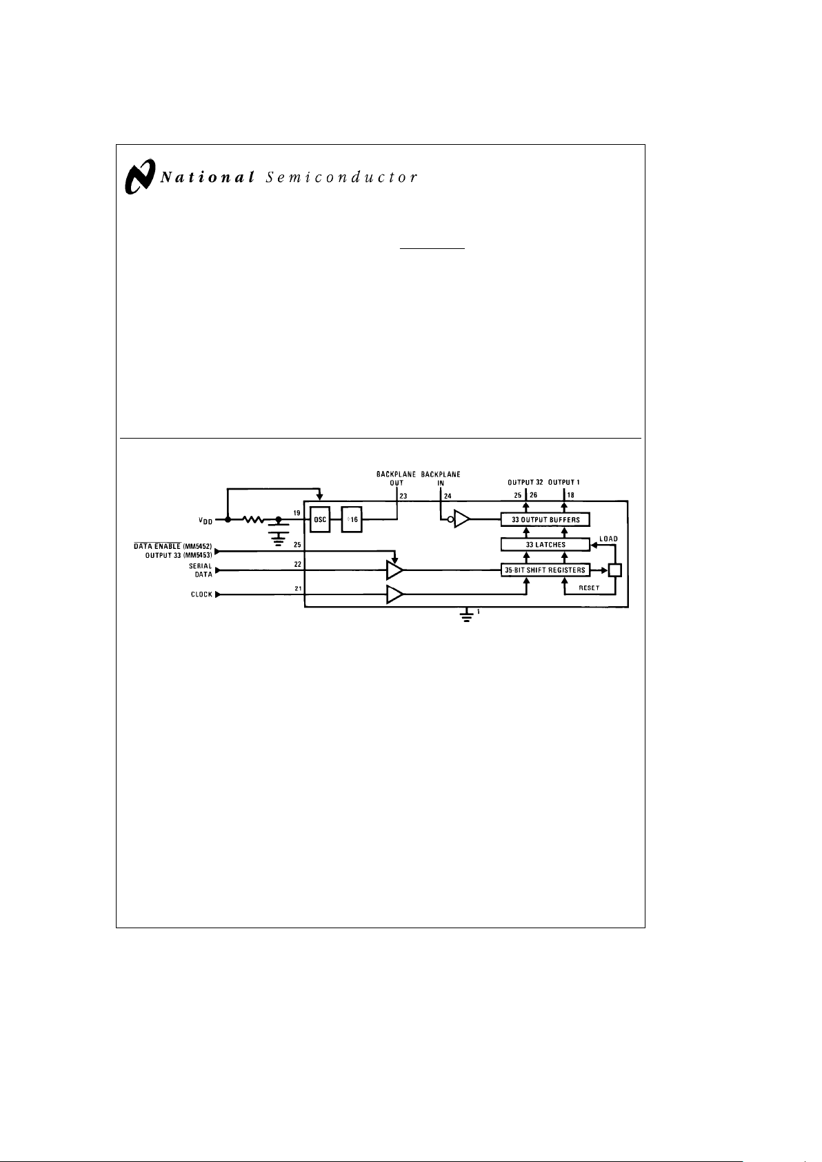
Block Diagram
TL/F/6137– 1
FIGURE 1
COPSTMis a trademark of National Semiconductor Corp.
C
1995 National Semiconductor Corporation RRD-B30M105/Printed in U. S. A.

Absolute Maximum Ratings
If Military/Aerospace specified devices are required,
please contact the National Semiconductor Sales
Office/Distributors for availability and specifications.
Voltage at Any Pin V
SS
to V
SS
a
10V
Operating Temperature 0§Ctoa70§C
Storage Temperature
b
65§Ctoa150§C
Power Dissipation 300 mW ata70§C
350 mW at
a
25§C
Junction Temperature
a
150§C
Lead Temperature (Soldering, 10 sec.) 300§C
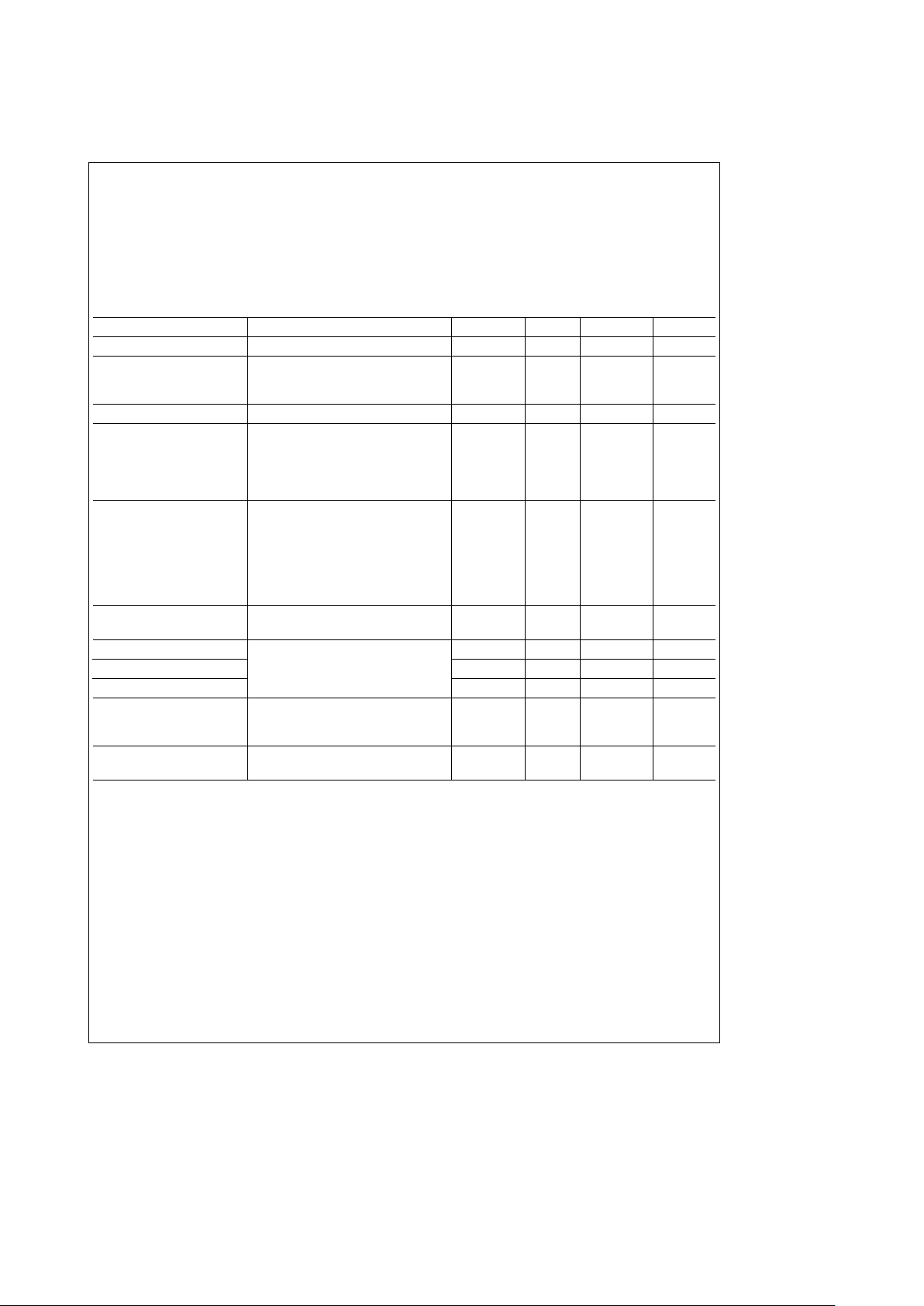
Electrical Characteristics
TAwithin operating range, V
DD
e
3.0V to 10V, V
SS
e
0V, unless otherwise specified
Parameter Conditions Min Typ Max Units
Power Supply 3 10 V
Power Supply Current Excluding Outputs
OSC
e
VSS,BPIN@32 Hz 40 mA
V
DD
e
5V, Open Outputs, No Clock 10 mA
Clock Frequency 500 kHz
Input Voltages
Logical ‘0’ Level V
DD
k
4.75
b
0.3 0.1 V
DD
V
V
DD
t
4.75
b
0.3 0.8 V
Logical ‘1’ Level V
DD
l
5.25 0.8 V
DD
V
DD
V
V
DD
s
5.25 2.0 V
DD
V
Output Current Levels
Segments
Sink V
DD
e
3V, V
OUT
e
0.3V
b
20 mA
Source V
DD
e
3V, V
OUT
e
V
DD
b
0.3V 20 mA
Backplane
Sink V
DD
e
3V, V
OUT
e
0.3V
b
320 mA
Source V
DD
e
3V, V
OUT
e
V
DD
b
0.3V 320 mA
Output Offset Voltage Segment Load 250 pF
g
50 mV
Backplane Load 8750 pF (Note 1)
Clock Input Frequency, f
C
(Notes 2 and 3) 500 kHz
High Time, t
h
950 ns
Low Time, t
l
950 ns
Data Input
Set-Up Time, t
DS
300 ns
Hold Time, t
DH
300 ns
Data Enable Input
100 ns
Set-Up Time, t
DES
Note 1: This parameter is guaranteed (not 100% production tested) over operating temperature and supply voltage ranges. Not to be used in Q.A. testing.
Note 2: AC input waveform for test purpose: t
r
s
20 ns, t
f
s
20 ns, fe500 kHz, 50%g10% duty cycle.
Note 3: Clock input rise and fall times must not exceed 300 ns.
2

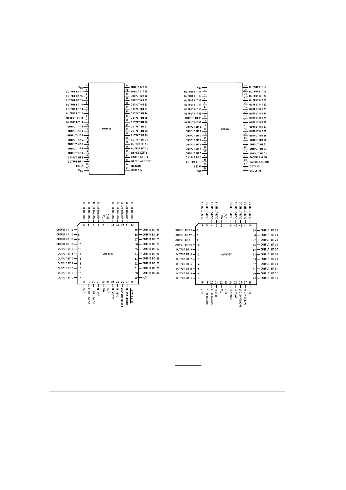
Connection Diagrams
Dual-In-Line Package
TL/F/6137– 2
Top View
FIGURE 2a
Plastic Chip Carrier
TL/F/6137– 11
Top View
Dual-In-Line Package
TL/F/6137– 3
Top View
FIGURE 2b
Plastic Chip Carrier
TL/F/6137– 12
Top View
Order Number MM5452N, MM5453N,
MM5452V or MM5453V
See NS Package Number N40A or V44A
Functional Description
The MM5452 is specifically designed to operate 4 (/2-digit 7segment displays with minimal interface with the display and
the data source. Serial data transfer from the data source to
the display driver is accomplished with 2 signals, serial data
and clock. Since the MM5452 does not contain a character
generator, the formatting of the segment information must
be done prior to inputting the data to the MM5452. Using a
format of a leading ‘‘1’’ followed by the 32 data bits allows
data transfer without an additional load signal. The 32 data
bits are latched after the 36th clock is complete, thus providing non-multiplexed, direct drive to the display. Outputs
change only if the serial data bits differ from the previous
time.
A block diagram is shown in
Figure 1.
For the MM5452 a
DATA ENABLE
is used instead of the 33rd output. If the
DATA ENABLE
signal is not required, the 33rd output can
be brought out. This is the MM5453 device.
3
 Loading...