NSC LP3913SQ-AA, LP3913 Datasheet

PRELIMINARY
March 2007
LP3913
Power Management IC for Flash Memory Based Portable
Media Players
General Description
The LP3913 is a programmable system power management
unit that is optimized for Flash Memory based Portable Media
Players.
The LP3913 incorporates 2 low-dropout LDO voltage regulators, 3 integrated Buck DC/DC converters with Dynamic Voltage Scaling (DVS), a 4-channel 8-bit A/D converter, and a
dual source Li-Ion/polymer battery charger. The charger has
the capability to charge and maintain a single cell battery from
a regulated wall adapter or USB power. When both USB and
adapter sources are present, then the adapter source takes
precedence and switching between USB and adapter power
sources is seamless. In addition, the battery charger supports
power routing, which allows system usage immediately after
an external power source has been detected. The LP3913
also incorporates some advanced battery management functions such as battery temperature measurement, reverse current blocking for USB, LED charger status indication,
thermally regulated internal power FETs, battery voltage
monitoring, over-current protection and a 10 hour safety
timer.
The 4-channel A/D converter measures the battery voltage
and charge current, which can be used for fuel gauging. Two
undedicated channels can be used to measure other analog
parameters such as discharge current, battery temperature,
keyboard resistor scanning and more.
The various IC parameters are programmable through a
400 kHz I2C compatible interface.
The LP3913 is available in a thermally-enhanced
6x6x0.8 mm 48 LLP package and operates over an ambient
temperature range of –40°C to +85°C.
Features
■
2 low-dropout regulators -- LDO1 is used for general
purpose applications, LDO2 is used for low-noise analog
applications. Both LDOs have programmable output
voltages.
■
Green and Red LED charger status drivers
■
4-channel 8-bit dual slope a/d converter
■
3 High-efficiency DVS Buck converters
■
400 kHz I2C compatible interface
■
Linear constant-current / constant-voltage charger for
single cell lithium-ion batteries
■
USB and Adapter charging
■
System power supply management
■
6x6x0.8mm 48 LLP package
■
Voltage and thermal supervisory circuits
■
Continuous battery voltage monitoring
■
Interrupt Request output with 8 sources
■
LP3913 is pin for pin and software compatible with the
LP3910 Hard Drive based PMIC
Key Specifications
■
LDO1: 150 mA, 1.2V–3.3V
■
LDO2: 150 mA, 1.3V–3.3V
■
Buck1: 600 mA, 0.8V–2.0V
■
Buck2: 600 mA, 1.8V–3.3V
■
Buck3: 500 mA, 1.8V–3.3V
■
50 mΩ battery path resistance
■
100 mA–1000 mA full-rate charge current using wall
adapter
■
Selectable 0.05C and 0.1C EOC current
■
USB current limit of 100 mA, 500 mA, and 800 mA
■
USB pre-qual current of 50 mA
■
Selectable 4.1V, 4.2V or 4.38V battery termination
voltages
■
0.35% battery termination accuracy
■
±1 LSB INL/DNL on 8-bit a/d converter
Applications
■
Flash-based portable media players
■
Portable gaming devices
■
Portable navigation systems
© 2007 National Semiconductor Corporation 300001 www.national.com
LP3913 Power Management IC for Flash Memory Based Portable Media Players
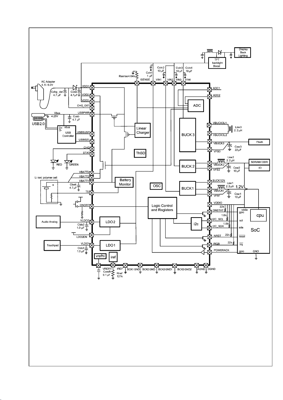
Typical Application Circuit
30000101
FIGURE 1. Application Diagram
www.national.com 2
LP3913
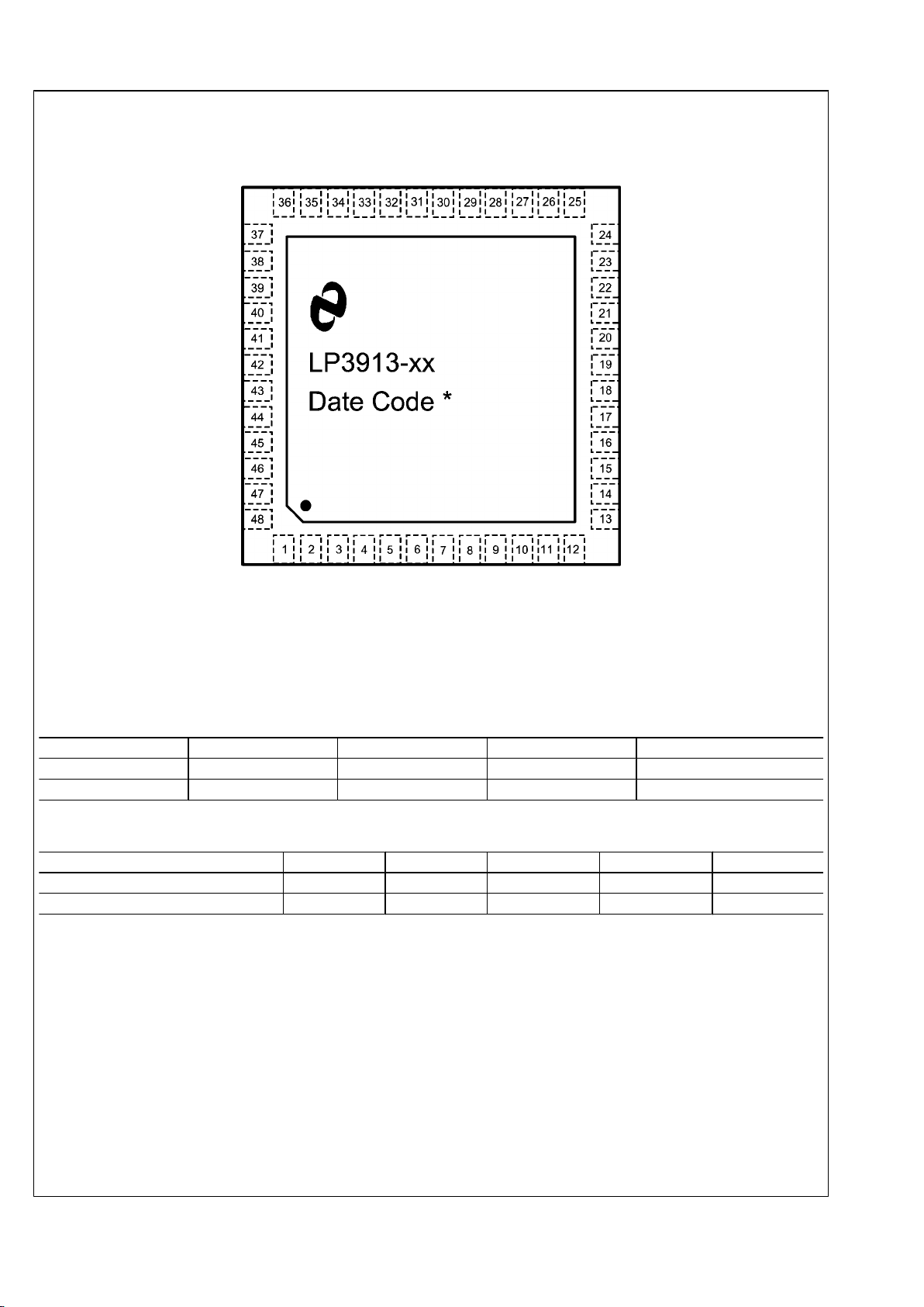
Connection Diagram
Device Connection Diagram
30000102
48 LLP Package (Top View)
SQF48A
The physical placement of the package marking will vary from
part to part.
(*) UZXYTT format: ‘U’ – wafer fab code; ‘Z’ – assembly code;
‘XY’ 2 digit date code; ‘TT’ – die run code
See http://www.national.com/quality/
marking_conventions.html for more information on marking
information.
Ordering Information
Order Number Package Type NSC Package Drawing Top Mark Supplied As
LP3913SQ-AA 48-lead LLP SQF48A LP3913SQ-AA 250 tape & reel
LP3913SQX-AA 48-lead LLP SQF48A LP3913SQX-AA 3000 tape & reel
Device Default Options
Order Number LDO1 LDO2 Buck1 Buck2 Buck3
LP3910SQ-AA 2.0V 3.3V 1.2V 3.3V 3.3V
LP3910SQX-AA 2.0V 3.3V 1.2V 3.3V 3.3V
3 www.national.com
LP3913
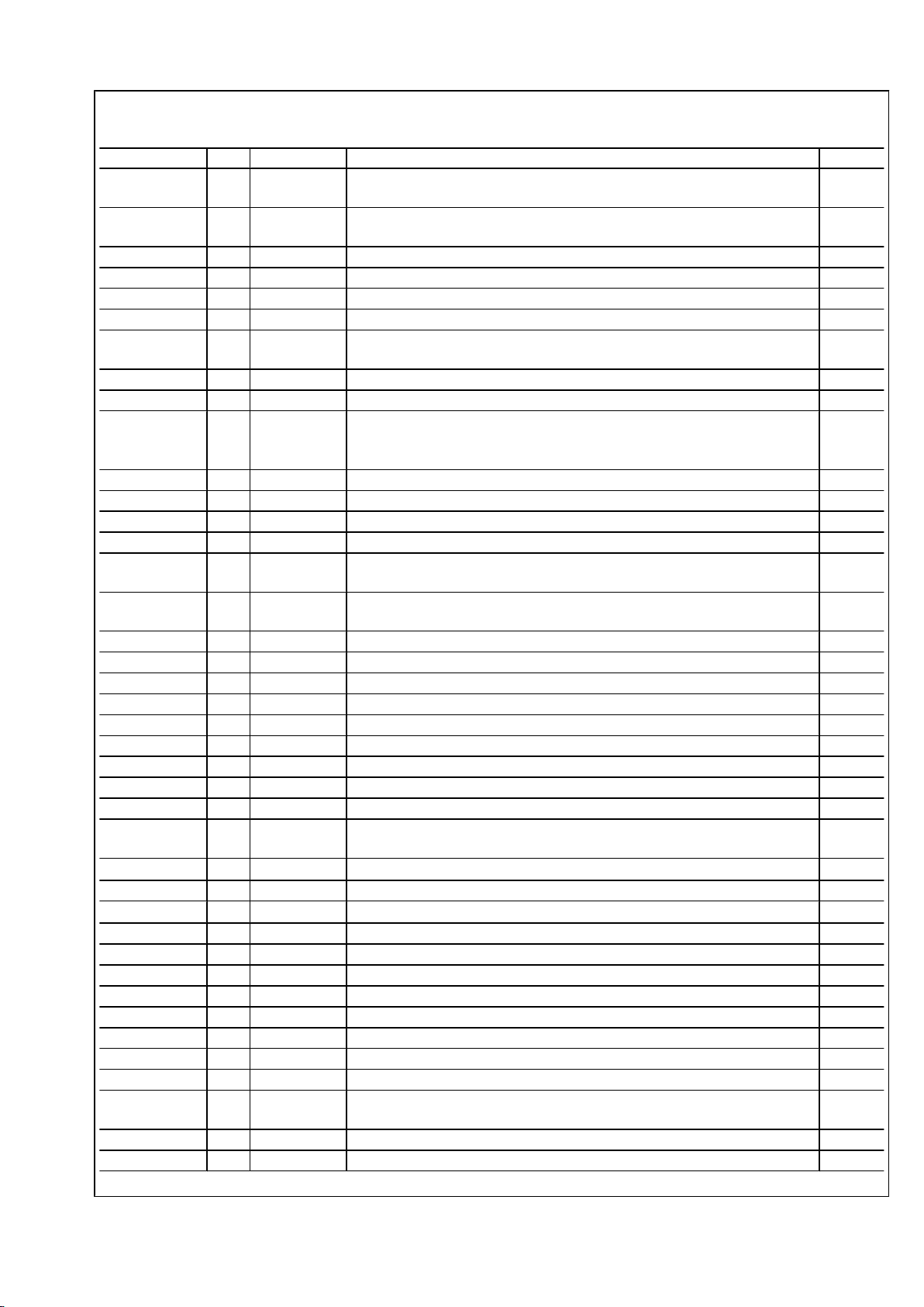
Pin Descriptions
Name I/O Type Functional Description Pin #
TS I A Battery temperature sense pin. This pin is normally connected to the thermistor
pin of the battery cell.
1
VBATT1 O A Positive battery terminal. This pin must be externally shorted to VBATT2 and
VBATT3
2
AGND G G Analog Ground 3
VREFH O A Connection to bypass capacitor for internal high reference 4
LDO2EN I D Digital input to enable/disable LDO2 5
VLDO2 O A LDO2 Output 6
VIN1 I PWR Power input to LDO1 and LDO2. VIN1 pin must be externally shorted to the VDD
pins.
7
VLDO1 O A LDO1 Output 8
POWERACK I D Digital power acknowledgement input (see Power Sequencing) 9
ISENSE I A
A 4.64 kΩ resistor must be connected between this pin and GND. A fraction of
the charge current flows through this resistor to enable the A to D converter to
measure the charge current.
10
ADC2 I A Channel 2 input to AD converter 11
ADC1 I A Channel 1 input to AD converter 12
IRQB O Open Drain Open drain active low interrupt request 13
NRST O Open Drain Open drain active low reset during Standby 14
CHG O D This output indicates that a valid charger supply source (USB adapter) has been
detected, and the IC is charging. (Red LED)
15
STAT O D Battery Status output indicator - Off during CC, 50% duty cycle during CV, 100%
duty cycle with a fully charged Li-ion battery (Green LED)
16
BUCK1EN I D Digital input to enable/disable BUCK1 17
VFB1 I A Buck1 Feedback input terminal 18
BCKGND1 G G Buck1 Ground 19
VBUCK1 O A Buck1 Output 20
VIN2 I PWR Power input to BUCK1. VIN2 pin must be externally shorted to the VDD pins. 21
VIN3 I PWR Power input to BUCK2. VIN3 pin must be externally shorted to the VDD pins. 22
VBUCK2 O A Buck2 Output 23
BCKGND2 G G Buck2 Ground 24
VFB2 I A Buck2 Feedback input terminal 25
ONOFF I D Power ON/OFF pin configured either as level (High or Low) triggered or edge
(High or Low) triggered.
26
I2C_SCL I D I2C compatible interface clock terminal 27
VDDIO I D Supply to input / output stages of digital I/O 28
I2C_SDA I/O D I2C compatible interface data terminal 29
ONSTAT O Open Drain Open Drain output that reflects the debounced state of ONOFF pin. 30
VFB3 I A Buck3 Feedback input terminal 31
VBUCK3 O A Buck3Output voltage 32
VBUCK3L2 I A Buck3 inductor 33
BCK3GND1 G G Buck3t high current ground 34
VBUCK3L1 I A Buck3 inductor 35
VIN4 I PWR Power input to Buck3. VIN4 pin must be externally shorted to the VDD pins. 36
USBSUSP I D This pin needs to be pulled high during USB suspend mode. 37
USBISEL I D Pulling this pin low limits the USB charge current to 100 mA. Pulling this pin high
limits the USB charge current to 500 mA.
38
BUCK3GND2 G G Buck3 Core Ground 39
DGND G G Digital ground 40
www.national.com 4
LP3913
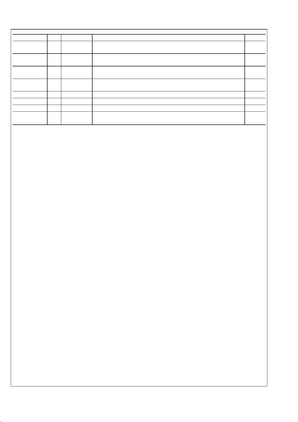
Name I/O Type Functional Description Pin #
VDD3 I PWR Power input to supply application. This pin must be externally shorted to VDD1
and VDD2.
41
VDD2 I PWR Power input to supply application This pin must be externally shorted to VDD1
and VDD3.
42
VBATT3 O A Positive battery terminal. This pin must be externally shorted to V\BATT1 and
VBATT2.
43
VBATT2 O A Positive battery terminal. This pin must be externally shorted to VBATT1 and
VBATT3.
44
USBPWR I PWR USB power input pin 45
VDD1 I PWR Power input to supply application This pin is shorted to VDD2 and VDD3. 46
CHG_DET I A Wall adapter power input pin 47
IREF I A
A 121 kΩ resistor must be connected between this pin and AGND. The resistor
value determines the reference current for the internal bias generator.
48
5 www.national.com
LP3913
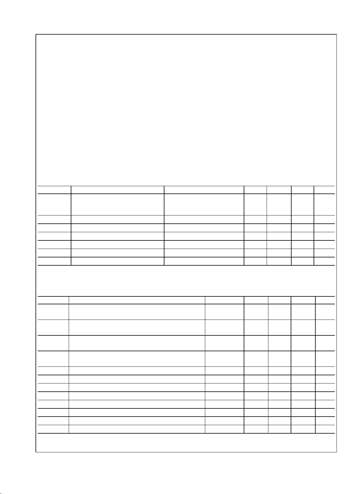
Absolute Maximum Ratings (Notes 1, 2)
If Military/Aerospace specified devices are required,
please contact the National Semiconductor Sales Office/
Distributors for availability and specifications.
Supply voltage range CHG_DET −0.3V to +6.5V
Voltage range USBPWR,
VIN1,VIN2,VIN3,VIN4,
VDD1,VDD2,VDD3 −0.3V to +6.2V
Battery voltage range VBATT1, 2, 3 −0.3V to +5V
All other pins −0.3V to VDD +0.3V
Storage Temperature Range −45ºC to +150ºC
Power Dissipation (TA = 70°C (Note 3)):
2.6W
ESD Rating (Note 4)
Human Body Model:
Machine Model:
2.0 kV
200V
Operating Ratings (Notes 6, 7, 10)
CHG_DET 4.5V to 6.0V
USBPWR 4.35V to 6.0V
VBATT1, 2, 3 0V to 4.5V
VIN1, VIN2, VIN3, VIN4, VDD1,
VDD2, VDD3
2.5V to 6.0V
VDDIO 2.5V to VDD
Junction Temperature (TJ) Range −40°C to +125°C
Ambient Temperature (TA) Range −40°C to +85°C
Power Dissipation for T
JjMAX
and T
AMAX
1.6W
Thermal Information
Junction-to-Ambient Thermal Resistance (θJA),
48-pin LLP SQF48A Package (Note 7)
25°C/W
Electrical Characteristics
General Electrical Characteristics
Unless otherwise noted, VDD = 5V, VBATT = 3.6V. Typical values and limits appearing in normal type apply for TJ = 25°C. Limits
appearing in boldface type apply over the entire junction temperature range for operation, TJ = 0°C to +125°C. (Notes 2, 7, 8, 9)
Symbol Parameter Conditions Min Typ Max Units
I
Q_BATT
Battery Standby Supply Current All circuits off except for POR and
battery monitor. No adapter or USB
power connected.
6 20 µA
V
POR
Power-On Reset Threshold VDD Falling Edge
1.9 V
T
SD
Thermal Shutdown Threshold
160 °C
T
SDH
Themal Shutdown Hysteresis
20 °C
T
TH-ALERT
Thermal Interrupt Threshold
115 °C
VDDIO IO Supply
2.5
V
DD
V
F
CLK
Internal System Clock Frequency
2 MHz
I2C Interface Electrical Characteristics
Unless otherwise noted, VDDIO = 3.6V. Typical values and limits appearing in normal type apply for TJ = 25°C. Limits appearing
in boldface type apply over the entire junction temperature range for operation, TJ = 0°C to +125°C. (Notes 2, 7, 8, 9)
Symbol Parameter Conditions Min Typ Max Units
V
IL
Low Level Input Voltage I2C_SDA &
I2C_SCL
0.3VDDI
O
V
V
IH
High Level Input Voltage I2C_SDA &
I2C_SCL
0.7VDDI
O
V
V
OL
Low Level Output Voltage I2C_SDA &
I2C_SCL
0
0.2VDDI
O
V
V
HYS
Schmitt Trigger Input Hysterisis I2C_SDA &
I2C_SCL
0.1VDDI
O
V
F
CLK
Clock Frequency
400 kHz
t
BF
Bus-Free Time between START and STOP (Note 9)
1.3 µs
t
HOLD
Hold Time Repeated START Condition (Note 9)
0.6 µs
t
CLK-LP
CLK Low Period (Note 9)
1.3 µs
t
CLK-HP
CLK High Period (Note 9)
0.6 µs
t
SU
Set-up Time Repeated START Condition (Note 9)
0.6 µs
t
DATA-HOLD
Data Hold Time (Note 9)
0 µs
t
DATA-SU
Data Set-up Time (Note 9)
100 ns
www.national.com 6
LP3913
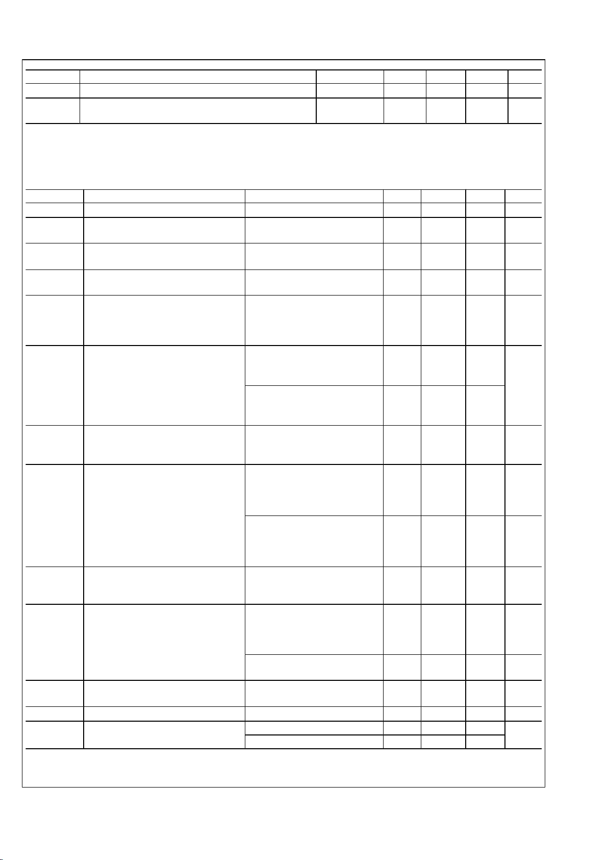
Symbol Parameter Conditions Min Typ Max Units
t
SU
Set-Up Time for STOP Condition (Note 9)
0.6 µs
t
TRANS
Maximum Pulse Width of Spikes That Must Be Suppressed
by the Input Filter of Both Data and CLK Signals.
(Note 9)
50 µs
Li-Ion Battery Charger Electrical Characteristics
Unless otherwise noted, VDD = 5.0V,VBATT = 3.6V, C
BATT
= 4.7 µF, C
CHG_DET
= 10 µF, R
IREF
= 121 kΩ. Typical values and limits
appearing in normal type apply for TJ = 25°C. Limits appearing in boldface type apply over the entire junction temperature range
for operation, TJ = 0°C to +125°C. (Notes 2, 6, 7, 8, 10)
Symbol Parameter Conditions Min Typ Max Units
V
USB
Minimum External USB Supply Soltage USB Current Limit = 500 mA
4.15 4.25 4.35 V
V
UVLO_USB
USBPWR Detect Input Under Voltage
Lockout
110 mV
CHG_DET Minimum External Adapter Supply
Voltage Range
Adapter Current Limit = 1A
V
FWD
Schottky = 350 mV
4.4 4.5 4.6 V
V
UVLO_CHG
CHG_DET Input
Under Voltage Lockout
150 mV
I
USB_SUSP
Quiescent Current in USB Suspend
Mode
USB Suspend Mode,
V
USB
= 5.0V
USBSUSP = USBPWR
USBISEL = 0V
30 60 µA
V
TERM_TOL
Battery Charge Termination Voltage
Tolerance
TA = 25°C,
I
PROG
= 500 mA
I
CHG
= 50 mA
-0.35
−0.5
−0.5
4.2V
4.1V
4.38V
+0.35
+0.5
+0.5
%
TA = 0°C to 125°C,
I
PROG
= 500 mA,
I
CHG
= 50 mA
−1
−1.5
−1.5
4.2V
4.1V
4.38V
+1
+1.5
+1.5
I
CHG_WA
Full-rate Charging Current from Wall
Adapter Input (See Full-rate Charging
Mode Description)
CHG_DET = 5.25V
V
BATT
= 3.6V
I
PROG
= 500 mA
450 500 550 mA
I
CHG_USB
Full-rate Charging Current from
USBPWR Input (See Full-rate Charging
Mode Description)
USB = 5V
V
BATT
= 3.6V
I
PROG
= 500 mA
USB_ISEL = 800 mA
450 500 550 mA
USB = 5V
V
BATT
= 3.6V
I
PROG
= 500 mA
USB_ISEL = 500 mA
405 450 495 mA
USB I
LIMIT
USB_ISEL = 100 mA
USB_ISEL= 500 mA
USB_ISEL = 800 mA
90
450
720
95
475
760
100
500
800
mA
I
PREQUAL
Pre-qualification Current V
BATT
= 2.5V, Wall Adapter Charge
Current.
Percentage of Programmed Full
Rate Current.
8 10 12
%
VBATT = 2.5V, USB Charge
Current
40 50 60 mA
V
FULL_RATE
Full-rate Qualification Threshold V
BATT
Rising, Transition from PreQualification to Full-rate Charging
2.75 2.85 2.95 V
V
TH_H
Upper TS Comparator Limit
2.82 2.87 2.93 V
V
TH_L
Lower TS Comparator Limit 45°C CHSPV Reg D3 = 0 0.315 0.33 0.345
V
50°C CHSPV Reg D3 = 1 0.255 0.27 0.285
7 www.national.com
LP3913
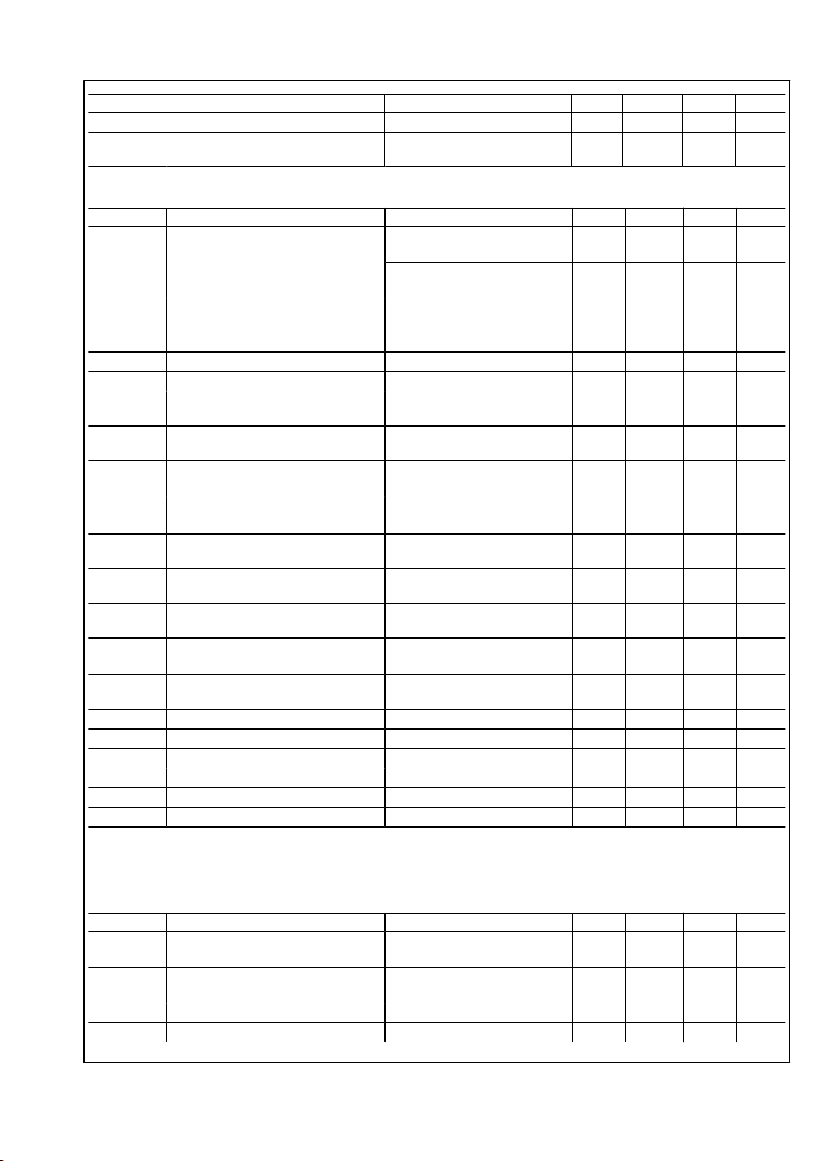
Symbol Parameter Conditions Min Typ Max Units
I
TSENSE
Battery Temperature Sense Current
7.75 8.00 8.25 µA
T
REG
Regulated Charger Junction
Temperature
105 115 125 °C
Detection and Timing
Symbol Parameter Conditions Min Typ Max Units
I
EOC
End-of-Charge Current I
PROG
= 500 mA,
10% EOC Setting
40 50 60 mA
I
PROG
= 500 mA
5% EOC Setting
20 25 30 mA
V
RESTARTl
Battery Restart Charging Voltage V
TERM
= 4.1V
V
TERM
= 4.2V
V
TERM
= 4.38V
3.82
3.94
4.14
3.9V
4.0V
4.2 V
3.94
4.06
4.26
V
T
CHG_IN
Deglitch Adapter Insertion
28 32 36 ms
T
USB
Deglitch USB Power Insertion
28 32 36 ms
T
PQ_FULL
Deglitch Time for Pre-qualification to Fullrate Charge Transition
8 10 12 ms
T
FULL_PQ
Deglitch Time for Full-rate to Prequalification Transition
8 10 12 ms
T
BATTLOWF
Deglitch Time for V
BATT
Falling below
V
BATTLOW
Threshold
4 5 6 ms
T
BATTLOWR
Deglitch Time for V
BATT
Rising above
V
BATTLOW
Threshold
4 5 6 ms
T
BATTEMP
Deglitch Time for Recovery from Battery
Temperature Fault
8 10 12 ms
T
ONOFF_F
Deglitching on Falling Edge of ONOFF
Pin
28 32 36 ms
T
ONOFF_R
Deglitching on Rising Edge of ONOFF
Pin
28 32 36 ms
T
RESTART
Deglitching on Falling V
BATT
Crossing
V
RESTART
8 10 12 ms
T
CCCV
Deglitching of CC->CV Charging
Transition
8 10 12 ms
T
CvEOC
Deglitching of CV->EOC (End of Charge)
8 10 12 ms
T
POWERACK
Deglitching of POWERACK Pin
4 5 6 ms
T
TSHD
Deglitching of Thermal Shutdown
2 ms
T
TOPOFF
Topoff Timer
17 21 25 min
T
10HR
10 Hour Safety Timer
9 10 11 hours
T
1HR
1 Hour Prequal Safety Timer
0.9 1 1.1 hour
Outputs Electrical Characteristics: CHG, STAT
Unless otherwise noted, VDD = 5V, V
BATT
= 3.6V. C
BATT
= 4.7 µF, C
CHG_DET
= 10 µF. Typical values and limits appearing in normal
type apply for TJ = 25°C. Limits appearing in boldface type apply over the entire junction temperature range for operation, TJ =
0°C to +125°C. (Notes 2, 6, 7, 8, 10)
Symbol Parameter Conditions Min Typ Max Units
I
LED
Output High Level V
LED
= 2.0V
CHSPV Register (02)h bit 5 = 1
4 5 6 mA
I
LED
Output High Level V
LED
= 2.0V
CHSPV Register (02)h bit 5 = 0
8 10 12 mA
I
LEAKAGE
Leakage Current V
LED
= 1.5V, LED off
0.1 5 µA
LED
FREQ
Blinking Frequency
0.8 1 1.2 Hz
www.national.com 8
LP3913
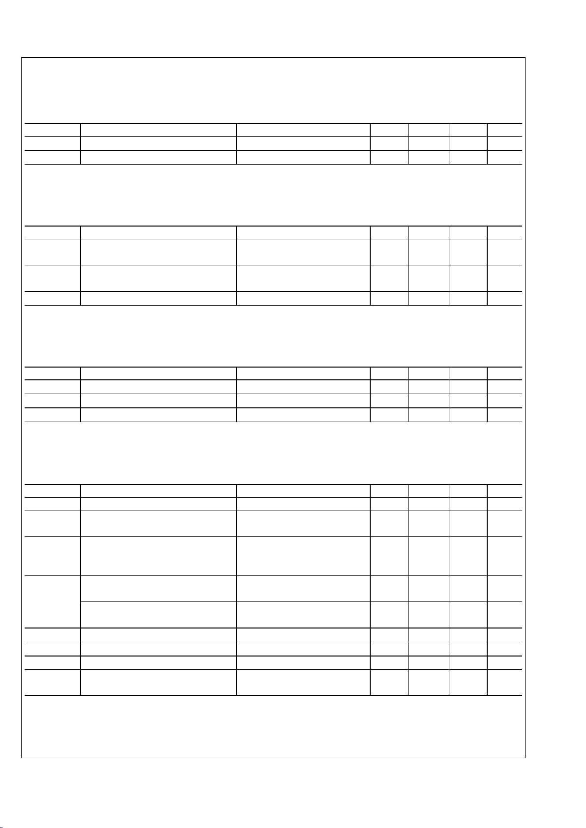
Outputs Electrical Characteristics: NRST, IRQB, ONSTAT
Unless otherwise noted, VDD = 5V, VBATT = 3.6V. C
BATT
= 4.7 µF, C
CHG_DET
= 10 µF. Typical values and limits appearing in
normal type apply for TJ = 25°C. Limits appearing in boldface type apply over the entire junction temperature range for operation,
TJ = 0°C to +125°C. (Notes 2, 6, 7, 8, 10)
Symbol Parameter Conditions Min Typ Max Units
V
OL
Output Low Level IOL = 4 mA
0.4 V
I
LEAKAGE
Leakage Current VDD = 2.5V, Output Logic High
−1 1 µA
Inputs Electrical Characteristics: USBSUSP, USBISEL
Unless otherwise noted, V
USB
= 5V, V
BATT
= 3.6V. C
BATT
= 4.7 µF, C
CHG_DET
= 10 µF. Typical values and limits appearing in normal
type apply for TJ = 25°C. Limits appearing in boldface type apply over the entire junction temperature range for operation, TJ =
0°C to +125°C. (Notes 2, 6, 7, 8, 10)
Symbol Parameter Conditions Min Typ Max Units
V
IL
Input Low Level
0.3*V
US
B
V
V
IH
Input High Level 0.7*V
US
B
V
I
LEAKAGE
Input Leakage
−1 1 µA
Inputs Electrical Characteristics: POWERACK, ONOFF, LDO2EN, BUCK1EN
Unless otherwise noted, VDD = 5V, V
BATT
= 3.6V. C
BATT
= 4.7 µF, C
CHG_IN
= 10 µF. Typical values and limits appearing in normal
type apply for TJ = 25°C. Limits appearing in boldface type apply over the entire junction temperature range for operation, TJ =
0°C to +125°C. (Notes 2, 6, 7, 8, 10)
Symbol Parameter Conditions Min Typ Max Units
V
IL
Input Low Level
0.4 V
V
IH
Input High Level
1.4 V
I
LEAKAGE
Input Leakage
−1 1 µA
LDO1: Low Drop Out Linear Regulators
Unless otherwise noted, VIN1 = 3.6V, I
MAX
= 150 mA, V
OUT
= Default Value, C
VDD
= 10 µF, C
LDO1
= 1.0 µF, ESR =
5 mΩ–500 mΩ, C
VREFH
= 100 nF. Typical values and limits appearing in normal type apply for TJ = 25°C. Limits appearing in
boldface type apply over the entire junction temperature range for operation, 0°C to +125°C.
Symbol Parameter Conditions Min Typ Max Units
VIN1 Operational Voltage Range 2.5 6.0 V
V
OUT
Range Output Voltage Programming Range TA = 25°C
1.2V–3.3V in 100 mV Steps
1.2 3.3 V
V
OUT
Accuracy
Output Voltage Accuracy
1 mA ≤ I
OUT
≤ I
MAX
, Over Full Line
and Load Regulation.
V
OUT
= Default Value.
−3 3 %
ΔV
OUT
Line Regulation VIN = (V
OUT
+ 500 mV) to 5.5V,
Load Current = I
MAX
3 mV
Load Regulation VIN = 3.6V,
Load Current = 1 mA to I
MAX
10 mV
I
SC
Short Circuit Current Limit V
OUT
= 0V
600 750 mA
VIN – V
OUT
Dropout Voltage Load Current = I
MAX
60 150 mV
PSRR Power Supply Ripple Rejection F = 10 kHz, Load Current = I
MAX
30 dB
R
SHUNT
LDO Output Impedance LDO Disabled, V
OUT
= Default
Value
200
Ω
9 www.national.com
LP3913
LDO2: Low Drop Out Linear Regulator
Unless otherwise noted VIN1 = 3.6V, I
MAX
= 150 mA, V
OUT
= Default Value, C
VDD
= 10.0 µF, C
LDO2
= 1.0 µF, ESR = 5 mΩ–
500 mΩ, C
VREFH
= 100 nF. Typical values and limits appearing in normal type apply for TJ = 25°C. Limits appearing in boldface
type apply over the entire junction temperature range for operation, 0°C to +125°C.
Symbol Parameter Conditions Min Typ Max Units
VIN2 Operational Voltage Range 2.5 6.0 V
V
OUT
Range Output Voltage Programming Range TA = 25°C
1.3V–3.3V in 100 mV Steps
1.3 3.3 V
V
OUT
Accuracy
Output Voltage Accuracy
(Default V
OUT
)
1 mA ≤ I
OUT
≤ I
MAX
, Over Full Line
and Load Regulation.
−3 3 %
ΔV
OUT
Line Regulation VIN = (V
OUT
+ 500 mV) to 5.5V,
Load Current = I
MAX
3 mV
Load Regulation VIN = 3.6V,
Load Current = 1 mA to I
MAX
10 mV
I
SC
Short Circuit Current Limit V
OUT
= 0V
600 750 mA
VIN – V
OUT
Dropout Voltage Load Current = I
MAX
60 150 mV
PSRR Power Supply Ripple Rejection F = 1 kHz, Load Current = I
MAX
50
dB
F = 10 kHz, Load Current = I
MAX
35
e
N
Analog Supply Output Noise Voltage 10 Hz < F < 100 kHz
50 µVrms
R
SHUNT
LDO Output Impedance LDO Disabled, V
OUT
= Default
Value
200
Ω
BUCK1 Converter Electrical Characteristics
Unless otherwise noted, VIN2 = 3.6 V, V
OUT
= default value, C
VIN2
= 10 µF, C
SW1
= 10 µF, L
SW1
= 2.2 µH Typical values and limits
appearing in normal type apply for TJ = 25°C. Limits appearing in boldface type apply over the entire junction temperature range
for operation, 0°C to +125°C. Modulation mode is PWM mode with automatic switch to PFM at light loads.
Symbol Parameter Conditions Min Typ Max Units
VIN2 Input Voltage 2.7 6.0 V
V
OUT
Range Output Voltage Programming Range 0.80V–2.00V in 50 mV Steps
0.8 2.0 V
ΔV
OUT
Static Output Voltage Tolerance I
OUT
= 200 mA, Including Line and
Load Regulation
−3 3 %
Line Regulation I
OUT
= 10 mA
V
IN2
= 2.5V − V
DD
0.2 %/V
Load Regulation 100 mA < I
OUT
< 300 mA
0.002 %/mA
I
OUT
Continuous Output Current 600 mA
Peak Output Current Limit 850 1000 1150 mA
I
PFM
Max I
LOAD
, PFM Mode
75 mA
I
Q
Quiescent Current I
OUT
= 0 mA
30 90
µA
Buck1 Disabled 1
F
OSC
Internal Oscillator Frequency PWM Mode
2 MHz
η
Peak Efficiency
90 %
T
ON
Turn-on Time To 95% Level (Note 9)
1 ms
BUCK2 Converter Electrical Characteristics
Unless otherwise noted, VIN3 = 3.6V, V
OUT
= default value, C
VIN3
= 10 µF, C
SW1
= 10 µF, L
SW2
= 2.2 µH Typical values and limits
appearing in normal type apply for TJ = 25°C. Limits appearing in boldface type apply over the entire junction temperature range
for operation, 0°C to +125°C. Modulation mode is PWM mode with automatic switch to PFM at light loads.
Symbol Parameter Conditions Min Typ Max Units
VIN3 Input Voltage 2.7 6.0 V
V
OUT
Range Output Voltage Programming Range 1.80V–3.30V in 100 mV Steps
1.8 3.3 V
www.national.com 10
LP3913
Symbol Parameter Conditions Min Typ Max Units
ΔV
OUT
Static Output Voltage Tolerance I
OUT
= 200 mA, Including Line and
Load Regulation
−3 3 %
Line Regulation I
OUT
= 10 mA
V
IN3
= 2.5V − V
DD
0.2 %/V
Load Regulation 100 mA < I
OUT
< 300 mA
0.002 %/mA
I
OUT
Continuous Output Current 600 mA
Peak Output Current Limit 780 1000 mA
I
PFM
Max I
LOAD
, PFM Mode
75 mA
I
Q
Quiescent Current I
OUT
= 0 mA
30 90
µA
Buck2 Disabled 1
F
OSC
Internal Oscillator Frequency PWM Mode
2 MHz
η
Peak Efficiency
90 %
T
ON
Turn-on Time To 95% Level (Note 9)
1 ms
BUCK3 Electrical Characteristics
Unless otherwise noted, VIN4 = 3.6V, C
VIN4
= 10 µF, CBB = 22 µF, LBB = 2.2 µH Typical values and limits appearing in normal type
apply for TJ = 25°C. Limits appearing in boldface type apply over the entire junction temperature range for operation, 0°C to +125°
C. Modulation mode is PWM mode with automatic switch to PFM at light loads.
Symbol Parameter Conditions Min Typ Max Units
VIN4 Input Voltage I
OUTMAX
= 500 mA
2.7 5.7 V
V
OUT
Range Output Voltage Programming Range 1.80V – 3.30V in 500 mV Steps
1.8 3.3 V
ΔV
OUT
Static Output Voltage Tolerance I
OUT
= 0 mA–500 mA, Including Line
and Load Regulation
−4 4 %
Line Regulation I
OUT
= 10 mA
0.2 %/V
Load Regulation 100 mA < I
OUT
< 500 mA
0.0016 %/mA
I
OUT
Continuous Output Current 500 mA
Peak Inductor Current Limit V
OUT
= 3.3V
1A Load at VIN = 2.7V
900 1200 mA
I
PFM
Max I
LOAD
, PFM Mode
75 mA
I
Q
Quiescent Current I
OUT
= 0 mA PFM No Switching
80
µA
Buck3 Disabled 1
F
OSC
Internal Oscillator Frequency PWM Mode
2 MHz
η
Peak Efficiency
93 %
T
ON
Turn-on Time To 95% Level (Note 9)
1 ms
ADC Electrical Characteristics
External components:
Symbol Parameter Conditions Min Typ Max Units
V
REF
Reference Voltage T = 25°C 1.220 1.225 1.230 V
T = 0°C to +125°C 1.200 1.225 1.230 V
INL Core ADC Integral Non-linearity V
REF
= 1.225 (Note 9)
-1 1 LSB
DNL Core ADC Differential Non-linearity V
REF
= 1.225 (Note 9)
-0.5 0.5 LSB
V
GP_IN
General Purpose ADC Input Voltage
Range
V
REF
2·V
REF
V
VBATT, Battery Max Voltage Scalar Output VBATT = 3.5V 2.435 2.45 2.465 V
RANGE 0
Battery Min Voltage Scalar Output VBATT = 2.6V
1.217 1.225 1.232 V
V
BATT,
Battery Max Voltage Scalar Output VBATT = 4.4V
2.435 2.45 2.465 V
RANGE 1
Battery Min Voltage Scalar Output V
REF
= 2.6V
1.217 1.225 1.232 V
11 www.national.com
LP3913
Symbol Parameter Conditions Min Typ Max Units
V
ISENSE
ISENSE Max Voltage Scalar Output V
ISENSE
= 0.6463V
(I
CHG
= 0.605A,
R
SENSE
= 4.64 kΩ)
2.373 2.45 2.519 V
RANGE 0
ISENSE Min Voltage Scalar Output V
ISENSE
= 0V
(I
CHG
= 0A,
R
SENSE
= 4.64 kΩ)
1.186 1.225 1.260 V
V
ISENSE
ISENSE Max Voltage Scalar Output V
ISENSE
= 1.175V
(I
CHG
= 1.1A,
R
SENSE
= 4.64 kΩ)
2.373 2.45 2.519 V
RANGE 1
ISENSE Min Voltage Scalar Output V
ISENSE
= 0V (I
CHG
= 0A,
R
SENSE
= 4.64 kΩ)
1.186 1.225 1.260 V
ADC1 &
ADC2
MIN
ADC1 & ADC2 Min Voltage Scalar Output V
REFH
= 1.225
1.218 1.225 1.230 V
ADC1 &
ADC2
MAX
ADC1 & ADC2 Max Voltage Scalar
Output
V
REFH
= 1.225
2.436 2.45 2.46 V
t
CONV
Conversion Time (Note 9)
5 ms
t
WARM
Warm-up Time
2 ms
Note 1: Absolute Maximum Ratings indicate limits beyond which damage to the component may occur. Operating Ratings are conditions under which operation
of the device is guaranteed. Operating Ratings do not imply guaranteed performance limits. For guaranteed performance limits and associated test conditions,
see the Electrical Characteristics tables.
Note 2: All voltages are with respect to the potential at the GND pin.
Note 3: Internal thermal shutdown circuitry protects the device from permanent damage. Thermal shutdown engages at TJ = 160°C (typ.) and disengages at T
J
= 140°C (typ.).
Note 4: The Human body model is a 100 pF capacitor discharged through a 1.5 kΩ resistor into each pin. The machine model is a 200 pF capacitor discharged
directly into each pin. MIL-STD-883 3015.7.
Note 5: In applications where high power dissipation and/or poor package thermal resistance is present, the maximum ambient temperature may have to be
derated. Maximum ambient temperature (T
A-MAX
) is dependent on the maximum operating junction temperature (T
J-MAX-OP
= 125°C), the maximum power
dissipation of the device in the application (P
D-MAX
), and the junction-to-ambient thermal resistance of the part/package in the application (θJA), as given by the
following equation: T
A-MAX
= T
J-MAX-OP
− (θJA × P
D-MAX
).
Note 6: Junction-to-ambient thermal resistance is highly application and board-layout dependent. In applications where high maximum power dissipation exists,
special care must be paid to thermal dissipation issues in board design.
Note 7: Min and Max limits are guaranteed by design, test, or statistical analysis. Typical numbers are not guaranteed, but do represent the most likely norm.
Note 8: Low ESR Surface-Mount Ceramic Capacitors (MLCCs) are used in setting electrical characteristics.
Note 9: Specifications guaranteed by design. Not tested during production.
Note 10: Typical values and limits appearing in normal type for TJ = 25°C. Limits appearing in boldface type apply over the entire junction temperature range
for operation, −40°C to +125°C.
Note 11: LDO2EN, BUCK1EN, and USBSUSP have weak internal pull downs while pins POWERACK, ONOFF do not have this.
www.national.com 12
LP3913
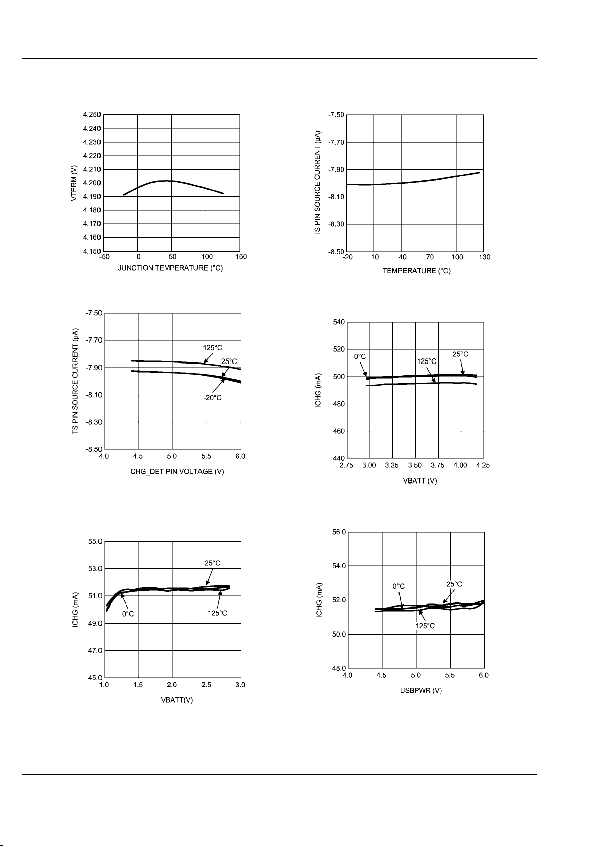
Typical Performance Characteristics — Battery Charger T
A
= 25°C unless otherwise noted
Vterm 4.2V vs. Temperature
30000196
TS Pin Current vs. Temperature
30000197
TS Pin Current vs. CHG_DET
30000198
ICHG vs. VBATT
CHG_DET = 5.0V, CC
30000199
ICHG vs. VBATT
CHG_DET = 5.0V, Prequal
I
PROG
= 500mA
30000139
ICHG vs. USBPWR
VBATT = 2.5V, Prequal
30000140
13 www.national.com
LP3913
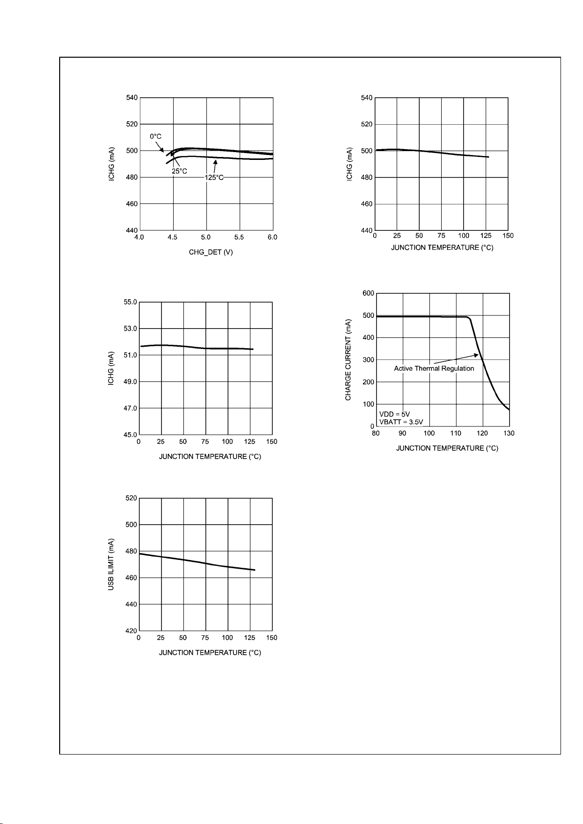
ICHG vs. CHG_DET
VBATT = 3.5V, CC
30000141
ICHG vs. Temperature
CHG_DET = 5V, VBATT = 3.75V, CC
30000142
ICHG vs. Temperature
CHG_DET = 5V, VBATT = 2.5V, Prequal
30000143
Thermal Regulation of Charge Current
30000144
USB ILIMIT vs. Temperature
30000145
www.national.com 14
LP3913
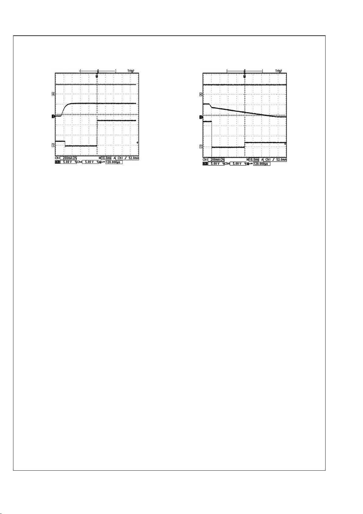
Wall Adapter Insertion with USBPWR present
CH1 = Charge Current (mA); CH3 = CHG_DET (V);
CH4 = USBPWR (V)
300001a0
Wall Adapter Removal with USBPWR present
CH1 = Charge Current (mA); CH3 = CHG_DET (V);
CH4 = USBPWR (V)
300001a1
15 www.national.com
LP3913
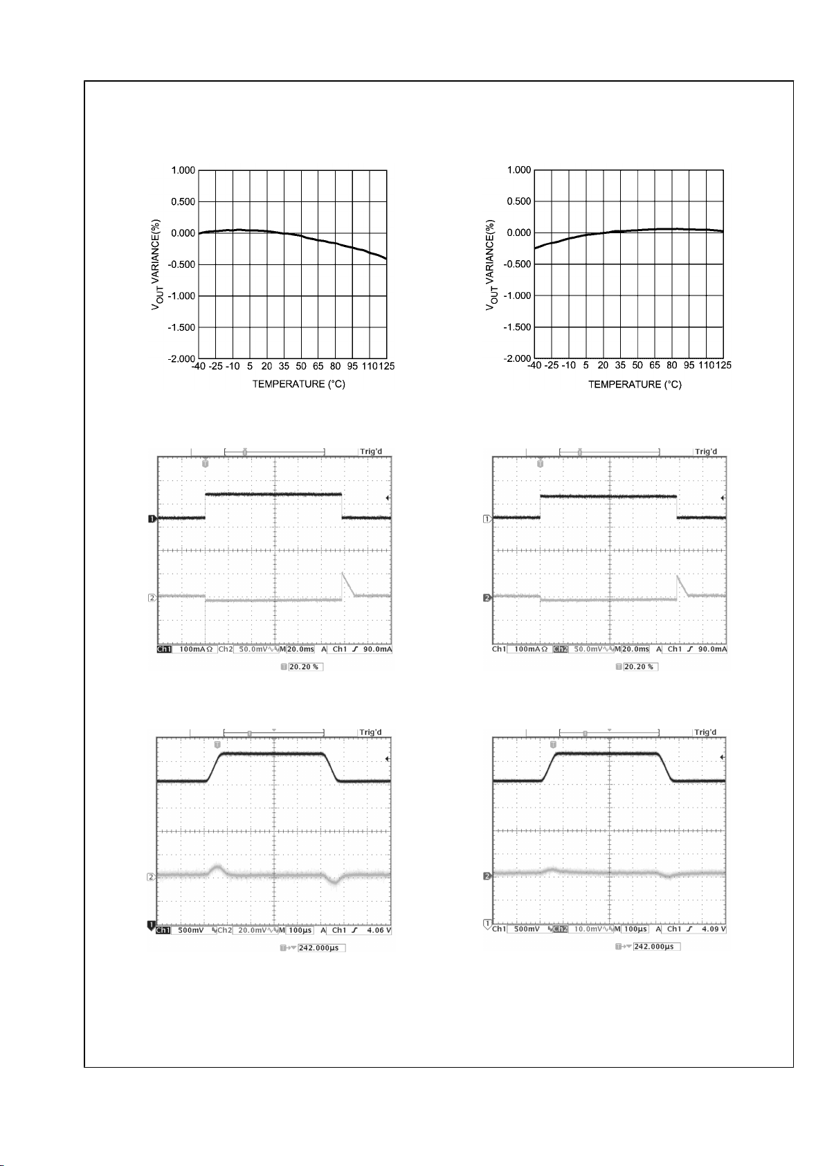
Typical Performance Characteristics — LDO T
A
= 25°C unless otherwise noted
Output Voltage Change vs Temperature (LDO1)
Vin = 4.3V, Vout = 3.3V, 100 mA load
30000146
Output Voltage Change vs Temperature (LDO2)
Vin = 4.3V, Vout = 1.8V, 100 mA load
30000147
Load Transient (LDO1)
3.6 Vin, 3.3 Vout, 0 – 100 mA load
30000148
Load Transient (LDO2)
3.6 Vin, 1.8 Vout, 0 – 100 mA load
30000149
Line Transient (LDO1)
3.6 - 4.5 Vin, 3.3 Vout, 150 mA load
30000150
Line Transient (LDO2)
3 – 4.2 Vin, 1.8 Vout, 150 mA load
30000151
www.national.com 16
LP3913
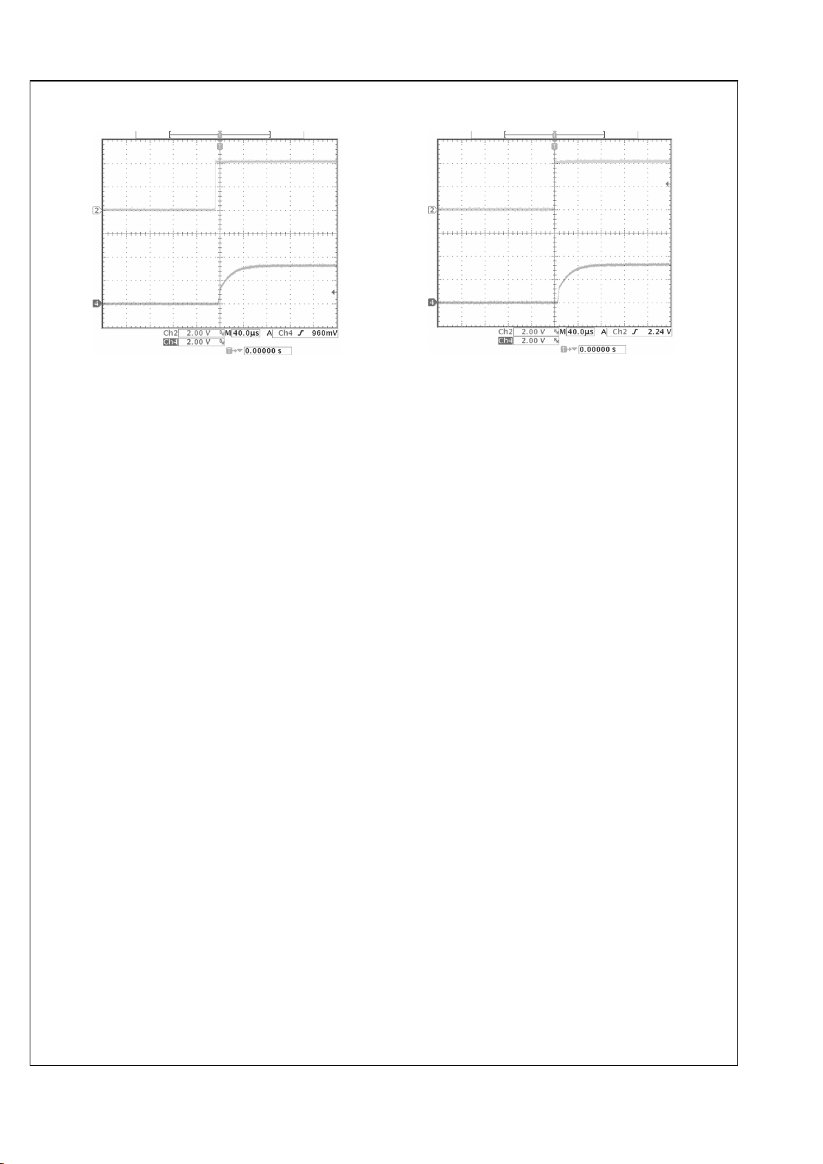
Enable Start-up time (LDO1)
0-3.6 Vin, 3.3 Vout, 1mA load
30000152
Enable Start-up time (LDO2)
0 – 3.6 Vin, 1.8 Vout, 1 mA load
30000153
17 www.national.com
LP3913
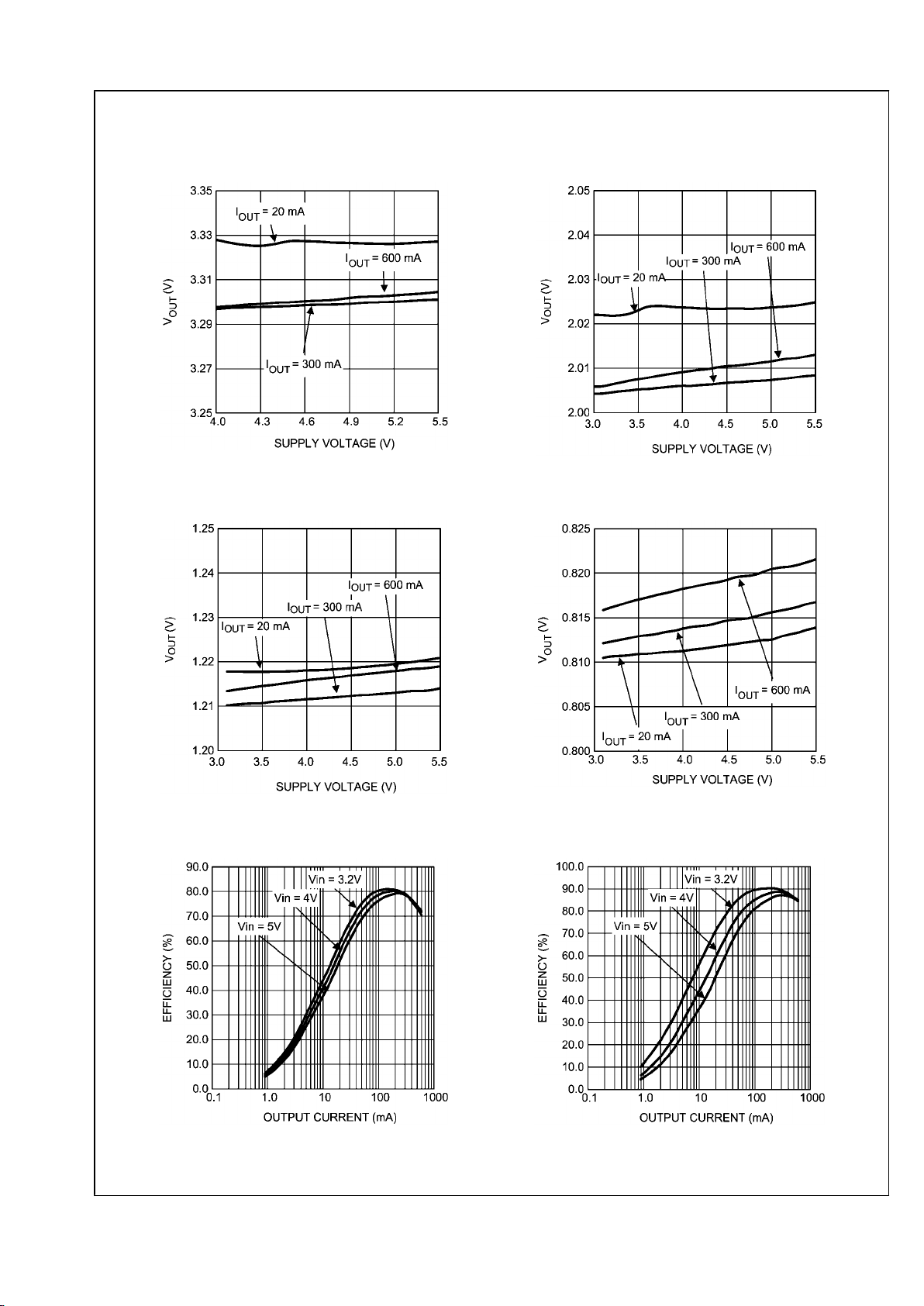
Typical Performance Characteristics - Buck T
A
= 25°C unless otherwise noted
Output Voltage vs. Supply Voltage
(Vout = 3.3 V)
30000154
Output Voltage vs. Supply Voltage
(Vout = 2.0 V)
30000155
Output Voltage vs. Supply Voltage
(Vout = 1.2V)
30000156
Output Voltage vs. Supply Voltage
(Vout = 0.8V)
30000157
Buck 1 Efficiency vs Output Current
(Forced PWM Mode, Vout =1.2V, L= 2.2µH)
30000158
Buck 1 Efficiency vs Output Current
(Forced PWM Mode, Vout =2.0V, L= 2.2µH)
30000159
www.national.com 18
LP3913
 Loading...