NSC LP3470M5-4.38, LP3470M5-4.00, LP3470M5-3.08, LP3470M5-2.63, LP3470IM5X-4.63 Datasheet
...
LP3470
Tiny Power On Reset Circuit
General Description
The LP3470 is a micropower CMOS voltage supervisory circuit designed to monitor power supplies in microprocessor
(µP) and other digital systems. It provides maximum adjustability forpower-on-reset(POR) and supervisory functions. It
is available in the following six standard reset threshold voltage (V
4.63V. If other voltage options between 2.4V and 5.0V are
desired please contact your National Semiconductor representative.
The LP3470 asserts a reset signal whenever the V
voltage falls below a reset threshold. The reset time-out period is adjustable using an external capacitor. Reset remains
asserted for an interval (programmed by an external capacitor) after V
The device is available in the tiny SOT23-5 package.
Key Specifications
n
n Standard Reset Threshold Voltages: 2.63V, 2.93V,
) options: 2.63V, 2.93V, 3.08V, 4.00V, 4.38V, and
RTH
has risen above the threshold voltage.
CC
±
1%Reset Threshold Accuracy Over Temperature
3.08V, 4.00V, 4.38V, and 4.63V
CC
supply
June 1999
n Custom Reset Threshold Voltages: For other voltages
between 2.4V and 5.0V contact your National
Semiconductor representative
n Very Low Quiescent Current (16 µA typical)
n Guaranteed Reset valid down to V
CC
=0.5V
Features
n Tiny SOT23-5 Package
n Open Drain Reset Output
n Programmable Reset Timeout Period Using an External
Capacitor
n Immune to Short V
Transients
CC
Applications
n Critical µP and µC Power Monitoring
n Intelligent Instruments
n Computers
n Portable/Battery-Powered Equipments
LP3470 Tiny Power On Reset Circuit
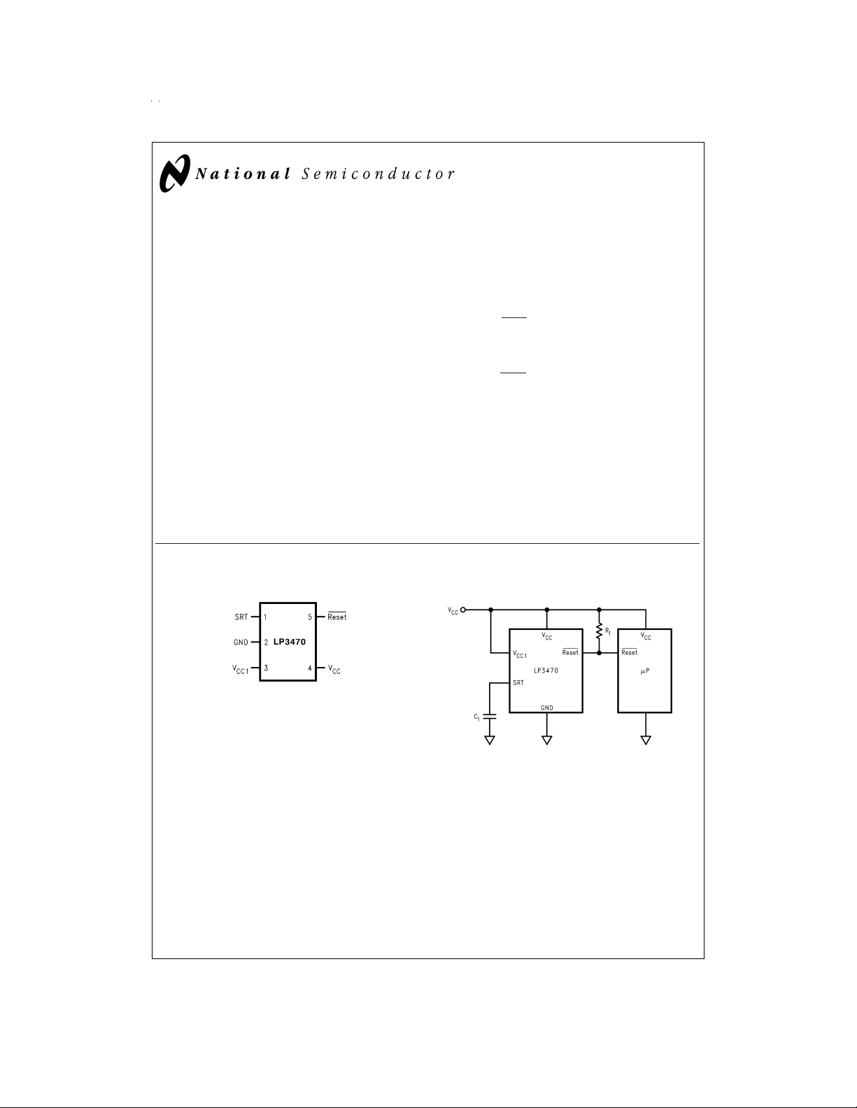
Pin Configuration and Basic Operating Circuit
Pin Configuration
DS100016-2
Top View
See NS Package Number
MA05B
Basic Operating Circuit
DS100016-1
© 1999 National Semiconductor Corporation DS100016 www.national.com

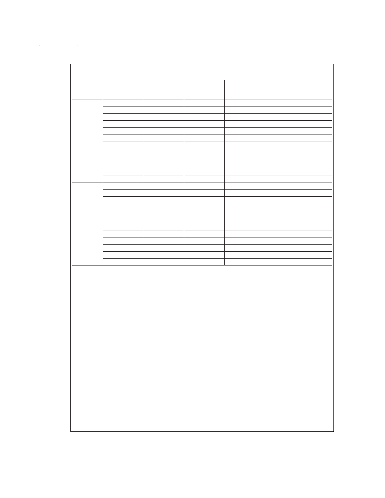
Ordering Information
Operating
Temperature
Range
−20˚C to
+85˚C
−40˚C to
+85˚C
Order
Number
LP3470M5-2.63 2.63 D25B SOT23-5 250 Units on Tape and Reel
LP3470M5X-2.63 2.63 D25B SOT23-5 3k Units on Tape and Reel
LP3470M5-2.93 2.93 D26B SOT23-5 250 Units on Tape and Reel
LP3470M5X-2.93 2.93 D26B SOT23-5 3k Units on Tape and Reel
LP3470M5-3.08 3.08 D28B SOT23-5 250 Units on Tape and Reel
LP3470M5X-3.08 3.08 D28B SOT23-5 3k Units on Tape and Reel
LP3470M5-4.00 4.00 D29B SOT23-5 250 Units on Tape and Reel
LP3470M5X-4.00 4.00 D29B SOT23-5 3k Units on Tape and Reel
LP3470M5-4.38 4.38 D30B SOT23-5 250 Units on Tape and Reel
LP3470M5X-4.38 4.38 D30B SOT23-5 3k Units on Tape and Reel
LP3470M5-4.63 4.63 D31B SOT23-5 250 Units on Tape and Reel
LP3470M5X-4.63 4.63 D31B SOT23-5 3k Units on Tape and Reel
LP3470IM5-2.63 2.63 D25C SOT23-5 250 Units on Tape and Reel
LP3470IM5X-2.63 2.63 D25C SOT23-5 3k Units on Tape and Reel
LP3470IM5-2.93 2.93 D26C SOT23-5 250 Units on Tape and Reel
LP3470IM5X-2.93 2.93 D26C SOT23-5 3k Units on Tape and Reel
LP3470IM5-3.08 3.08 D28C SOT23-5 250 Units on Tape and Reel
LP3470IM5X-3.08 3.08 D28C SOT23-5 3k Units on Tape and Reel
LP3470IM5-4.00 4.00 D29C SOT23-5 250 Units on Tape and Reel
LP3470IM5X-4.00 4.00 D29C SOT23-5 3k Units on Tape and Reel
LP3470IM5-4.38 4.38 D30C SOT23-5 250 Units on Tape and Reel
LP3470IM5X-4.38 4.38 D30C SOT23-5 3k Units on Tape and Reel
LP3470IM5-4.63 4.63 D31C SOT23-5 250 Units on Tape and Reel
LP3470IM5X-4.63 4.63 D31C SOT23-5 3k Units on Tape and Reel
Nominal
(V)
V
RTH
Package
Marking
Package
Type
Supplied As
www.national.com 2

Absolute Maximum Ratings (Note 1)
If Military/Aerospace specified devices are required,
please contact the National Semiconductor Sales Office/
Distributors for availability and specifications.
V
Voltage −0.3V to +6V
CC
Reset Voltage
Output Current (Reset)
−0.3V to +6V
10 mA
Operating Temperature Range
LP3470 −20˚C to +85˚C
LP3470I −40˚C to +85˚C
Junction Temperature (T
Power Dissipation (T
2)
(Note 2) 280˚C/W
θ
JA
) 125˚C
Jmax
= 25˚C) (Note
A
300 mW
Storage Temp. Range −65˚C to +150˚C
Lead Temp. (Soldering, 5 sec) 260˚C
ESD Rating (Note 3) 2 kV
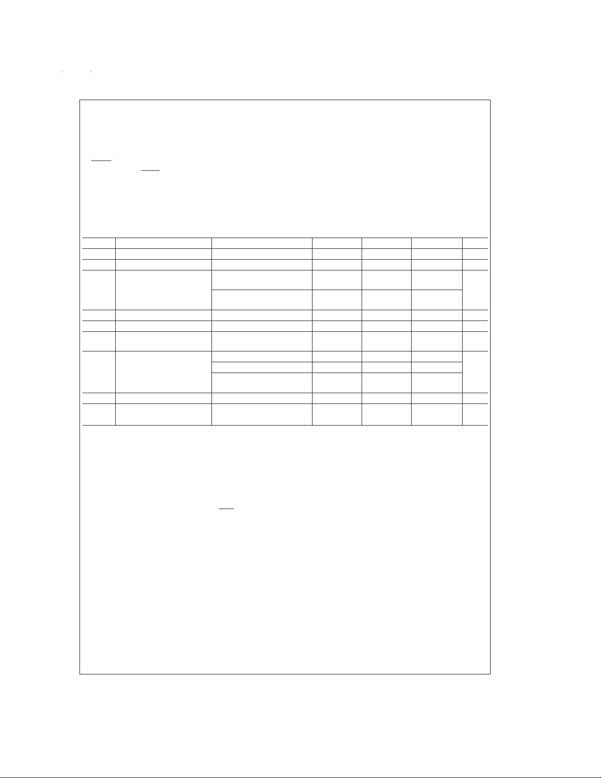
Electrical Characteristics
Limits in standard typeface are for TJ= 25˚C, and limits in boldface type apply over the full operating temperature range, unless
otherwise specified. VCC= +2.4V to +5.0V unless otherwise noted.
Symbol Parameter Conditions Typ (Note 4) Min (Note 5) Max (Note 5) Units
V
I
V
V
t
t
V
R
I
CC
CC
RTH
HYST
PD
RP
OL
1
LEAK
Operating Voltage Range 0.5 5.5 V
VCCSupply Current VCC= 4.5V 16 30 µA
Reset Threshold Voltage
(Note 6)
LP3470 V
LP3470I V
RTH
RTH
0.99 V
0.99 V
0.99 V
0.985 V
RTH
RTH
RTH
RTH
1.01 V
1.01 V
1.01 V
1.015 V
RTH
RTH
RTH
RTH
Hysteresis Voltage (Note 7) 35 15 65 mV
VCCto Reset Delay VCCfalling at 1 mV/µs 100 300 µs
Reset Timeout Period (Note8)C1=1nF 2 1.0 3.5
Reset Output Voltage Low VCC= 0.5V; IOL=30µA 0.1
= 1.0V; IOL= 100 µA 0.1
V
CC
V
CC=VRTH
mA
−100 mV; IOL=4
0.4
External Pull-up Resistor 20 0.68 68 kΩ
Reset Output Leakage
Current
Note 1: Absolute Maximum Ratings indicate limits beyond which damage to the device may occur. Electrical specifications do not apply when operating the device
beyond its operating conditions.
Note 2: The maximum power dissipation must be derated at elevated temperatures and is dictated by T
bient Thermal Resistance), and T
given in the Absolute Maximum Ratings, whichever is lower.
Note 3: The Human Body Model is a 100 pF capacitor discharged through a 1.5 kΩ resistor into each pin.
Note 4: Typical numbers are at 25˚C and represent the most likely parametric norm.
Note 5: Min. and Max. limits in standard typeface are 100%production tested at 25˚C. Min. and Max. limits in boldface are guaranteed through correlation using Sta-
tistical Quality Control (SQC) methods. The limits are used to calculate National’s Average Outgoing Quality Level (AOQL).
Note 6: Factory-trimmed reset thresholds are available in 50 mV increments from 2.4V to 5.0V. Contact your National Semiconductor representative.
Note 7: V
Note 8: tRPis programmable by varying the value of the external capacitor (C1) connected to pin SRT. The equation is: tRP=2000xC1(C1in µF and tRPin ms).
affects the relation between VCCand Reset as shown in the timing diagram.
HYST
(Ambient Temperature).Themaximum allowable power dissipation at any temperature is P
A
0.15 1
(Maximum Junction Temperature),θJA(Junction to Am-
Jmax
Dmax
=(T
Jmax−TA
)/ θJAor the number
6
V
ms
V
µA
www.national.com3
 Loading...