NSC LMX2347TM, LMX2347SLBX, LMX2347MDC, LMX2347EVAL Datasheet
LMX2346/LMX2347
PLLatinum
™
Frequency Synthesizer for RF Personal
Communications
LMX2346 2.0 GHz
LMX2347 2.5 GHz
General Description
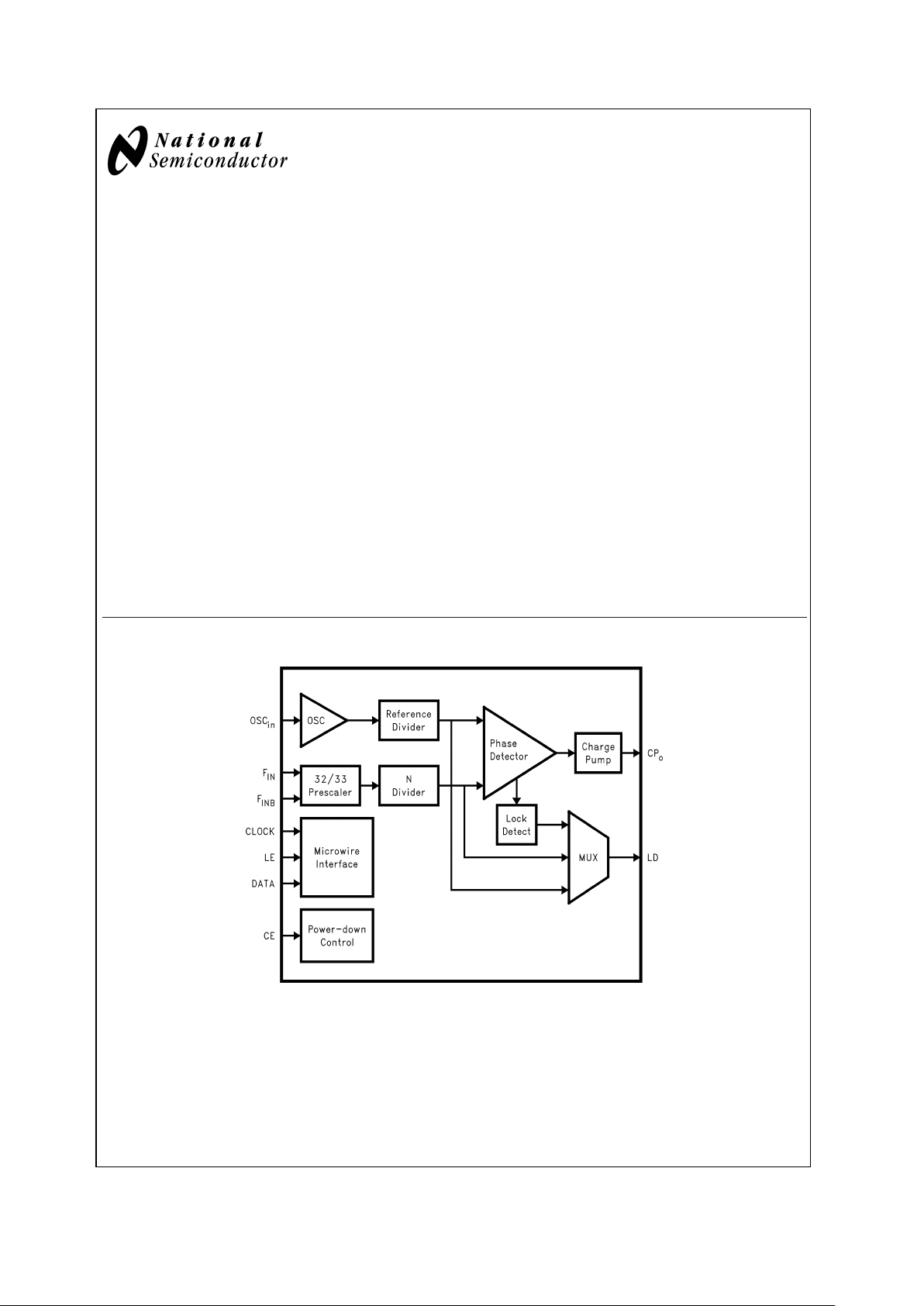
The LMX2346/7 are high performance frequency synthesizers with an integrated 32/33 dual modulus prescaler. The
LMX2346 is designed for RF operation up to 2.0 GHz. The
LMX2347 is designed for RF operation up to 2.5 GHz. Using
a proprietary digital phase locked loop technique, the
LMX2346/7 generates very stable, low noise control signals
for UHF and VHF voltage controlled oscillators.
Serial data is transferred into the LMX2346/7 via a three-line
MICROWIRE interface (DATA, LE, CLOCK). Supply voltage
range is from 2.7V to 5.5V. The charge pump provides 4 mA
output current.
The LMX2346/7 are manufactured using National’s 0.5µ
ABiC V silicon BiCMOS process and is available in 16-pin
TSSOP and 16-pin CSP packages.
Features
n RF operation up to 2.5 GHz
n 2.7V to 5.5V operation
n Digital & Analog Lock Detect
n 32/33 Dual modulus prescaler
n Excellent Phase Noise
n Internal balanced, low leakage charge pump
n Pin Compatible to LMX2323
Applications
n Cellular DCS/PCS/3G infrastructure equipment
n Wireless Local Area Networks (WLANs)
n Other wireless communication systems
Functional Block Diagram
20038406
PLLatinum™is a trademark of National Semiconductor Corporation.
November 2002
LMX2346/LMX2347 PLLatinum Frequency Synthesizer for RF Personal Communications
© 2002 National Semiconductor Corporation DS200384 www.national.com
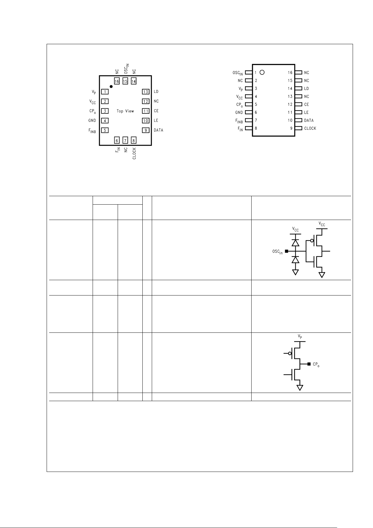
Connection Diagrams
20038407
16-Pin Chip Scale Package
NS Package Number SLB16A
20038401
16-Pin TSSOP Package
NS Package Number MTC16
Pin Descriptions
Pin Name
Pin Number
I/O Description I/O Circuit Configuration
16-Pin
CSP
16-Pin
TSSOP
OSC
IN
15 1 I Reference oscillator input. A CMOS
inverting gate input. The input has a
V
CC
/2 input threshold and can be driven
from an external CMOS or TTL logic
gate.
V
P
1 3 — Charge Pump Power Supply. Must be
equal to V
CC
.
V
CC
2 4 — Main Power Supply. VCCmay range from
2.7V to 5.5V. Bypass capacitors should
be placed as close as possible to this pin
and be connected directly to the ground
plane.
CP
o
3 5 O Charge Pump output. For connection to a
loop filter for driving the voltage control
input of an external VCO.
GND 4 6 — Ground.
LMX2346/LMX2347
www.national.com 2
Pin Descriptions (Continued)
Pin Name
Pin Number
I/O Description I/O Circuit Configuration
16-Pin
CSP
16-Pin
TSSOP
F
INB
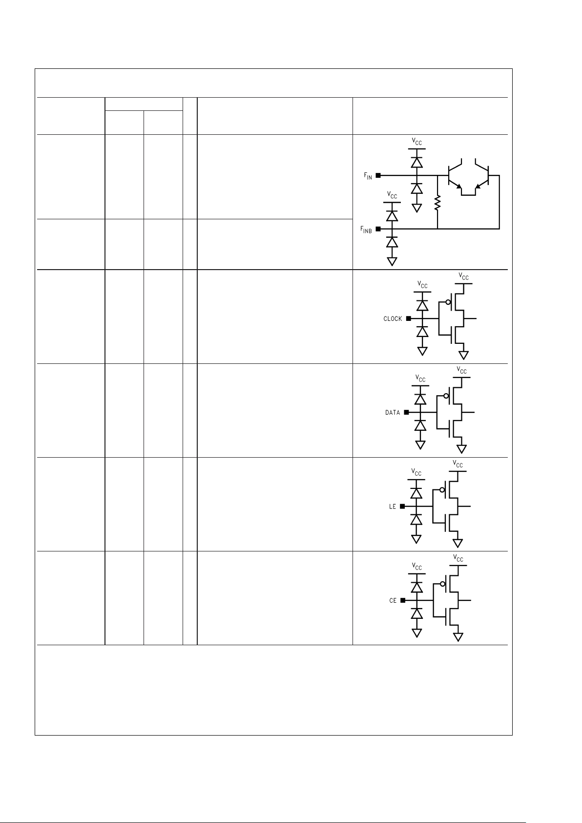
5 7 I RF prescaler complementary input. For
single ended operation, this pin should be
AC grounded. The LMX2346/7 can be
driven differentially when a bypass
capacitor is omitted.
F
IN
6 8 I RF PLL prescaler input. Small signal
input from the VCO.
CLOCK 8 9 I High impedance CMOS Clock input. Data
is clocked in on the rising edge, into the
18-bit shift register.
DATA 9 10 I Binary serial data input. Data entered
MSB first. LSB is control bit. High
impedance CMOS input.
LE 10 11 I Latch Enable input. When Latch Enable
transitions HIGH, data stored in the 18-bit
shift register is loaded into one of the 2
control registers, based on the address
bit. High impendance CMOS input.
CE 11 12 I Chip Enable input. Provides logical
power-down control of the device. Pull-up
to V
CC
if unused. High impedance CMOS
input.
LMX2346/LMX2347
www.national.com3
Pin Descriptions (Continued)
Pin Name
Pin Number
I/O Description I/O Circuit Configuration
16-Pin
CSP
16-Pin
TSSOP
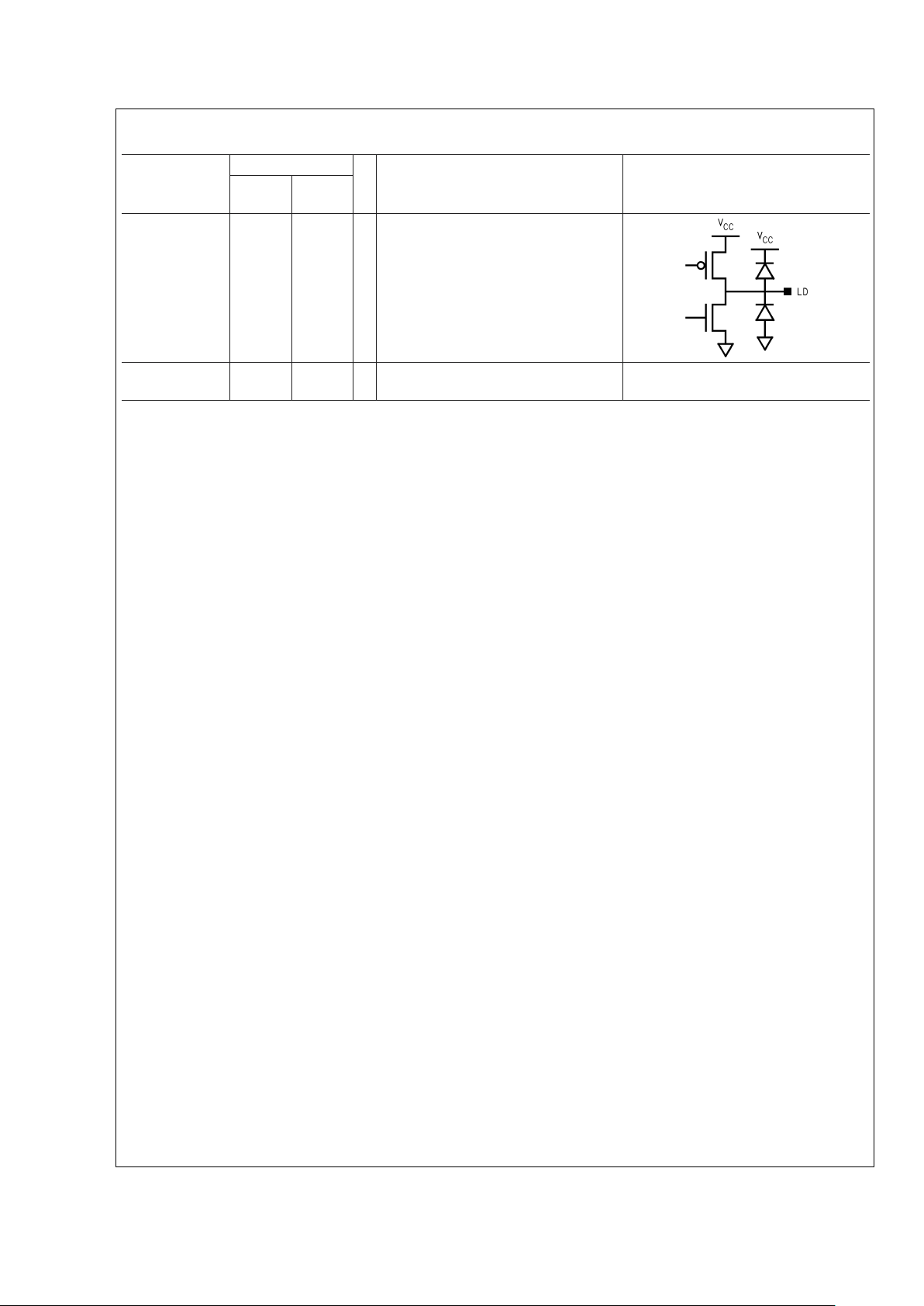
LD 13 14 O Locked Detect output. Multi-function
CMOS output pin that provides
multiplexed access to digital lock detect,
open-drain analog lock detect, as well as
the outputs of the R and N counters.
NC 7, 12, 14,162, 13, 15,16No Connect.
LMX2346/LMX2347
www.national.com 4
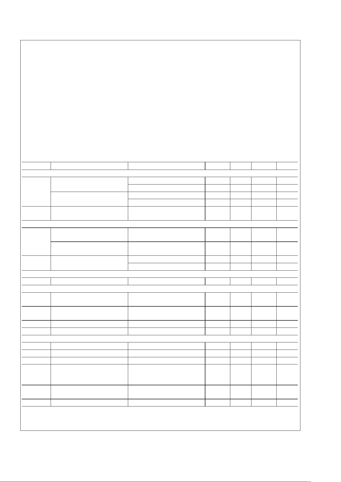
Absolute Maximum Ratings (Notes 1,
2)
If Military/Aerospace specified devices are required,
please contact the National Semiconductor Sales Office/
Distributors for availability and specifications.
Power Supply Voltage,
(V
CC
) −0.3V to +6.5V
Power Supply for Charge
Pump, (V
P
) −0.3V to +6.5V
Voltage on any pin with
GND=0V, (V
i
) −0.3V to VCC+0.3V
Storage Temperature
Range, (TS) −65˚C to +150˚C
Lead Temp. (solder 4 sec.),
(T
L
) +260˚C
Recommended Operating
Conditions
(Note 1)
Min Max Unit
Power Supply Voltage, (V
CC
) 2.7 5.5 V
Power Supply for Charge Pump, (V
P
) 2.7 5.5 V
(V
P
must be equal to VCC)
Operating Temperature, (T
A
) −40 +85 ˚C
Electrical Characteristics
The following conditions apply; VCC=VP= 3.0V; −40˚C ≤ TA≤ 85˚C, unless specified differently.
Symbol Parameter Conditions Min Typ Max Units
I
CC
I
CC
Power Supply Current, LMX2346 3.5 4.5 mA
V
CC
= 5.5V 7.0 mA
Power Supply Current, LMX2347 4.5 5.5 mA
V
CC
= 5.5V 8.0 mA
I
CC
-pwdn Power Down Current CLOCK, DATA, LE = GND
CE = GND
110µA
RF PRESCALER
F
IN
Operating Frequency, RF
Prescaler, LMX2346
0.2 2.0 GHz
Operating Frequency, RF
Prescaler, LMX2347
0.2 2.5 GHz
PF
IN
Input Sensitivity, RF Prescaler 2.7V ≤ VCC≤ 3.0V (Note 6) −15 +0 dBm
3.0V
<
VCC≤ 5.5V (Note 6) −10 +0 dBm
PHASE DETECTOR
F
φ
Phase Detector Frequency 10 MHz
REFERENCE OSCILLATOR
F
OSC
Operating Frequency, Reference
Oscillator Input
(Note 10)
5 104 MHz
V
OSC
Input Sensitivity, Reference
Oscillator Input
(Note 7)
0.4 V
CC
− 0.3 V
PP
I
IH
OSCinHigh-Level Input Current VIH=VCC= 5.5V 100 µA
I
IL
OSCinLow-Level Input Current VIL= 0V, VCC= 5.5V −100 µA
CHARGE PUMP
ICPo-
source
Charge Pump Source Current VCPo = Vp/2V −4.0 mA
ICPo-
sink
Charge Pump Sink Current VCPo = Vp/2V 4.0 mA
ICPo-
tri
Charge Pump TRI-STATE Current 0.5V ≤ VCPo ≤ VP− 0.5V −2.5 2.5 nA
ICPo-
sink
vs.
ICPo-
source
CP Sink vs. Source Mismatch VCPo = Vp/2
T
A
= 25˚
(Note 4)
310%
ICPo vs
VCPo
CP Current vs. Voltage 0.5V ≤ VCPo ≤ V
P
− 0.5V
T
A
= 25˚ (Note 4)
10 15 %
ICPo vs T
A
CP Current vs. Temperature VCPo = Vp/2V (Note 4) 10 %
LMX2346/LMX2347
www.national.com5

Electrical Characteristics (Continued)
The following conditions apply; VCC=VP= 3.0V; −40˚C ≤ TA≤ 85˚C, unless specified differently.
Symbol Parameter Conditions Min Typ Max Units
LOGICAL INTERFACE (CE, CLOCK, LE, DATA, LD)
V
IH
High-level Input Voltage 0.8 V
CC
V
V
IL
Low-level Input Voltage 0.2 V
CC
V
I
IH
High-level Input Current VIH=VCC= 5.5V −1.0 1.0 µA
I
IL
Low-level Input Current VIL= 0V, VCC= 5.5V −1.0 1.0 µA
V
OH
High-level Output Voltage IOH= −500 µA VCC− 0.4 V
V
OL
Low-level Output Voltage IOL= 500 µA 0.4 V
MICROWIRE INTERFACE (CLOCK, LE, DATA)
t
CS
Data to Clock Set Up Time (Note 5) 50 ns
t
CH
Data to Clock Hold Time (Note 5) 10 ns
t
CWH
Clock Pulse Width High (Note 5) 50 ns
t
CWL
Clock Pulse Width Low (Note 5) 50 ns
t
ES
Clock to Latch Enable Set Up
Time
(Note 5)
50 ns
t
EW
Latch Enable Pulse Width (Note 5) 50 ns
PHASE NOISE
L(f) Single Side-Band Phase Noise F
IN
= 900 MHz
F
φ
= 200 kHz
F
OSC
= 10 MHz
V
OSC
= 1.0 V
PP
TA= 25˚C (Note 3)
−91 dBc/Hz
F
IN
= 1750 MHz
F
φ
= 200 kHz
F
OSC
= 10 MHz
V
OSC
= 1.0 V
PP
TA= 25˚C (Notes 3, 9)
−86 dBc/Hz
F
IN
= 1960 MHz
F
φ
= 200 kHz
F
OSC
= 10 MHz
V
OSC
= 1.0 V
PP
TA= 25˚C (Note 3)
−85 dBc/Hz
F
IN
= 2450 MHz
F
φ
= 200 kHz
F
OSC
= 10 MHz
V
OSC
= 1.0 V
PP
TA= 25˚C (Note 3)
−83 dBc/Hz
L
N
(f) Normalized Single Side-Band
Phase Noise
Fφ= 200 kHz
F
OSC
= 10 MHz
V
OSC
= 1.0 V
PP
TA= 25˚C (Note 8)
−164.5 dBc/Hz
Note 1: Absolute Maximum Ratings indicate limits beyond which damage to the device may occur. Recommended Operating Conditions indicate conditions for
which the device is intended to be functional. For guaranteed specifications and test conditions see the Electrical Characteristics.
Note 2: This device is a high performance RF integrated circuit with an ESD rating
<
2 kV. Handling and assembly of this device should only be done at ESD
protected workstations.
Note 3: Phase Noise is measured using a reference evaluation board with a loop bandwidth of approximately 12 kHz. The phase noise specification is the
composite average of 3 measurements made at frequency offsets of 2.0, 2.5 and 3.0 kHz.
Note 4: See Charge Pump Measurement Definitions for detail on how these measurements are made.
Note 5: See Serial Input Data Timing.
Note 6: See F
IN
Sensitivity Test Setup.
Note 7: See OSC
in
Sensitivity Test Setup.
Note 8: Normalized Single-Side Band Phase Noise is defined as: L
N
(f) = L(f) − 20 log (FIN/Fφ), where L(f) is defined as the Single Side-Band Phase Noise.
Note 9: This parameter is derived from Normalized Single Side-Phase Noise, L
n
(f).
Note 10: For F
OSC
frequencies below 10 MHz, it is recommended that the rise time of the signal does not exceed 25ns.
LMX2346/LMX2347
www.national.com 6
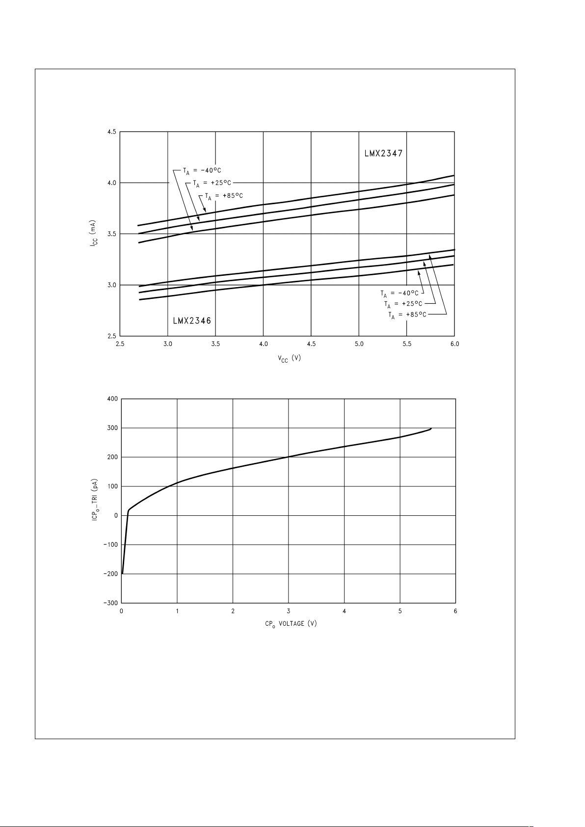
Typical Performance
Characteristics
ICCvs VCCLMX2346/7
20038422
CPOTRI-STATE vs CPOVoltage at 85˚C
20038423
LMX2346/LMX2347
www.national.com7
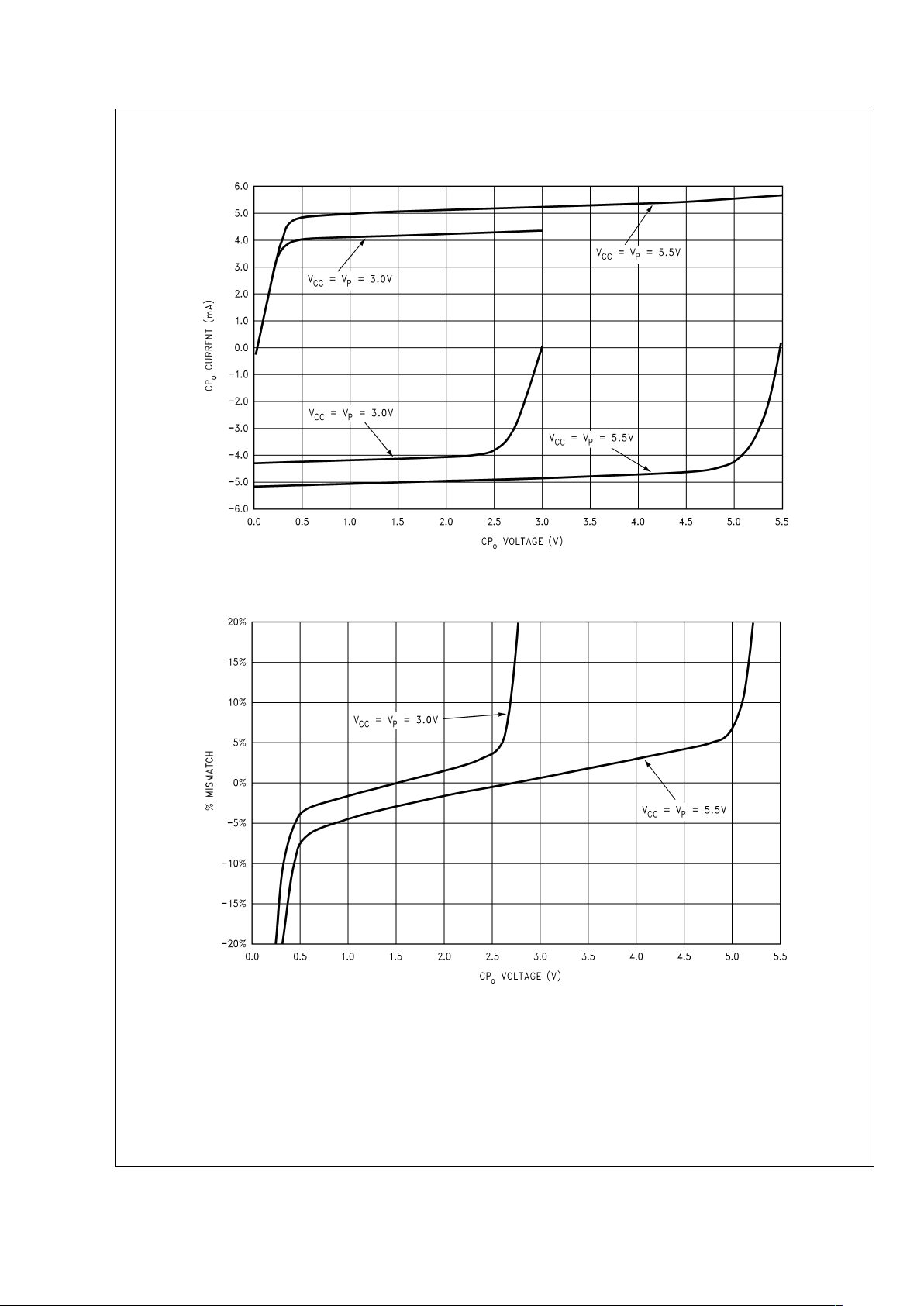
Typical Performance Characteristics (Continued)
LMX2346/7 Charge Pump Sweeps
20038424
Sink vs Source Mismatch
(See forumla under Charge Pump Current Specifications Definitions)
20038425
LMX2346/LMX2347
www.national.com 8
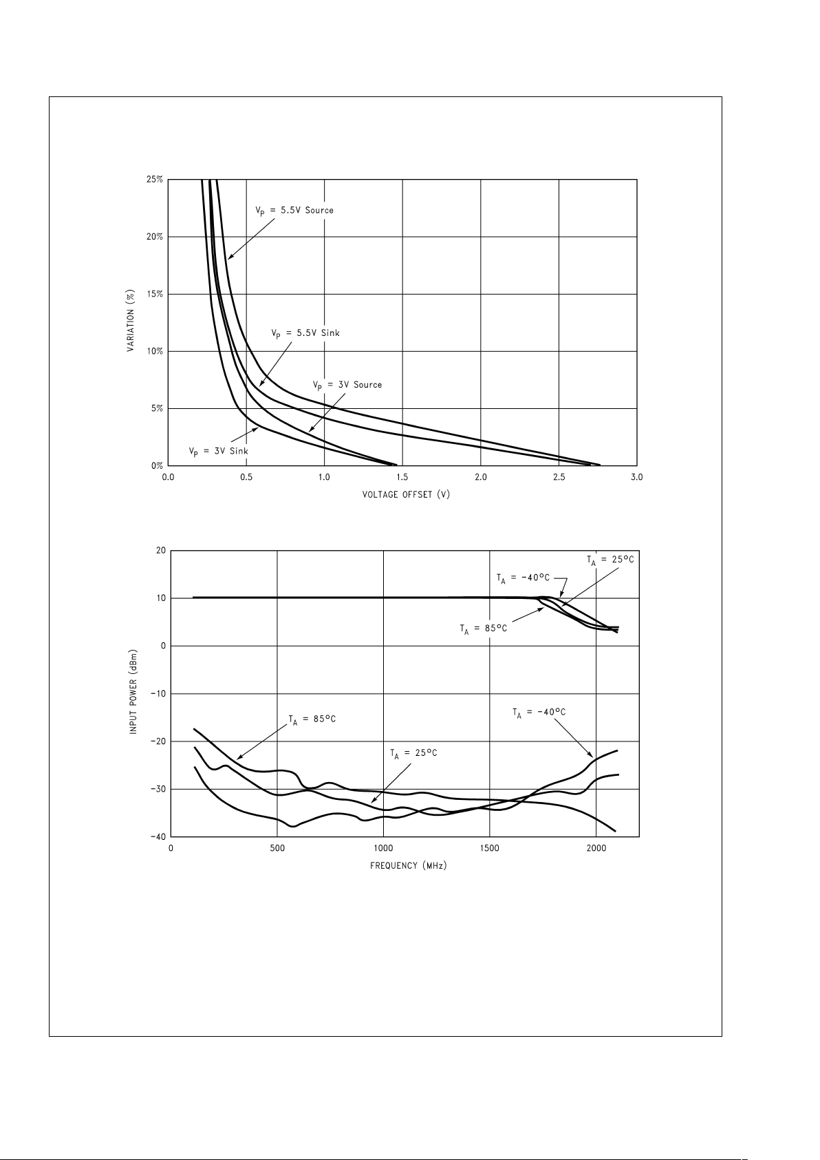
Typical Performance Characteristics (Continued)
Charge Pump Current Variation
(See forumla under Charge Pump Current Specifications Definitions)
20038426
LMX2346 FINSensitivity vs Frequency at 3.0V
20038427
LMX2346/LMX2347
www.national.com9
 Loading...