

NSC LMX2332LTMX, LMX2332LSLDX, LMX2332LSLBX Datasheet

LMX2330L/LMX2331L/LMX2332L
October 2001
LMX2330L/LMX2331L/LMX2332L PLLatinum Low Power Dual Frequency Synthesizer for RF
Personal Communications
PLLatinum
™
Low Power Dual Frequency Synthesizer for
RF Personal Communications
LMX2330L 2.5 GHz/510 MHz
LMX2331L 2.0 GHz/510 MHz
LMX2332L 1.2 GHz/510 MHz
General Description
The LMX233XL family of monolithic, integrated dual frequency synthesizers, including prescalers, is to be used as a
local oscillator for RF and first IF of a dual conversion
transceiver. It is fabricated using National’s 0.5µ ABiC V
silicon BiCMOS process.
The LMX233XL contains dual modulus prescalers. A 64/65
or a 128/129 prescaler (32/33 or 64/65 in the 2.5 GHz
LMX2330L) can be selected fortheRFsynthesizeranda8/9
or a 16/17 prescaler can be selected for the IF synthesizer.
LMX233XL, which employs a digitalphase locked looptechnique, combined with a high quality reference oscillator,
provides the tuning voltages for voltage controlled oscillators
to generate very stable, low noise signals for RFand IF local
oscillators. Serial data is transferred into the LMX233XL via
a three wire interface (Data, Enable, Clock). Supply voltage
can range from 2.7V to5.5V.The LMX233XL family features
very low current consumption;
LMX2330L—5.0 mA at 3V, LMX2331L —4.0 mA at 3V,
LMX2332L—3.0 mA at 3V.
The LMX233XL are available in a TSSOP 20-pin, CSP
24-pin surface mount plastic package, and thin CSP 20-pin
surface mount plastic package.
Features
n Ultra low current consumption
n 2.7V to 5.5V operation
n Selectable synchronous or asynchronous powerdown
mode:
I
= 1 µA typical at 3V
CC
n Dual modulus prescaler:
LMX2330L (RF) 32/33 or 64/65
LMX2331L/32L (RF) 64/65 or 128/129
LMX2330L/31L/32L (IF) 8/9 or 16/17
n Selectable charge pump TRI-STATE
n Selectable charge pump current levels
n Selectable Fastlock
n Upgrade and compatible to LMX233XA family
™
mode
®
mode
Applications
n Portable Wireless Communications
(PCS/PCN, cordless)
n Cordless and cellular telephone systems
n Wireless Local Area Networks (WLANs)
n Cable TV tuners (CATV)
n Other wireless communication systems
Functional Block Diagram
01280601
© 2001 National Semiconductor Corporation DS012806 www.national.com
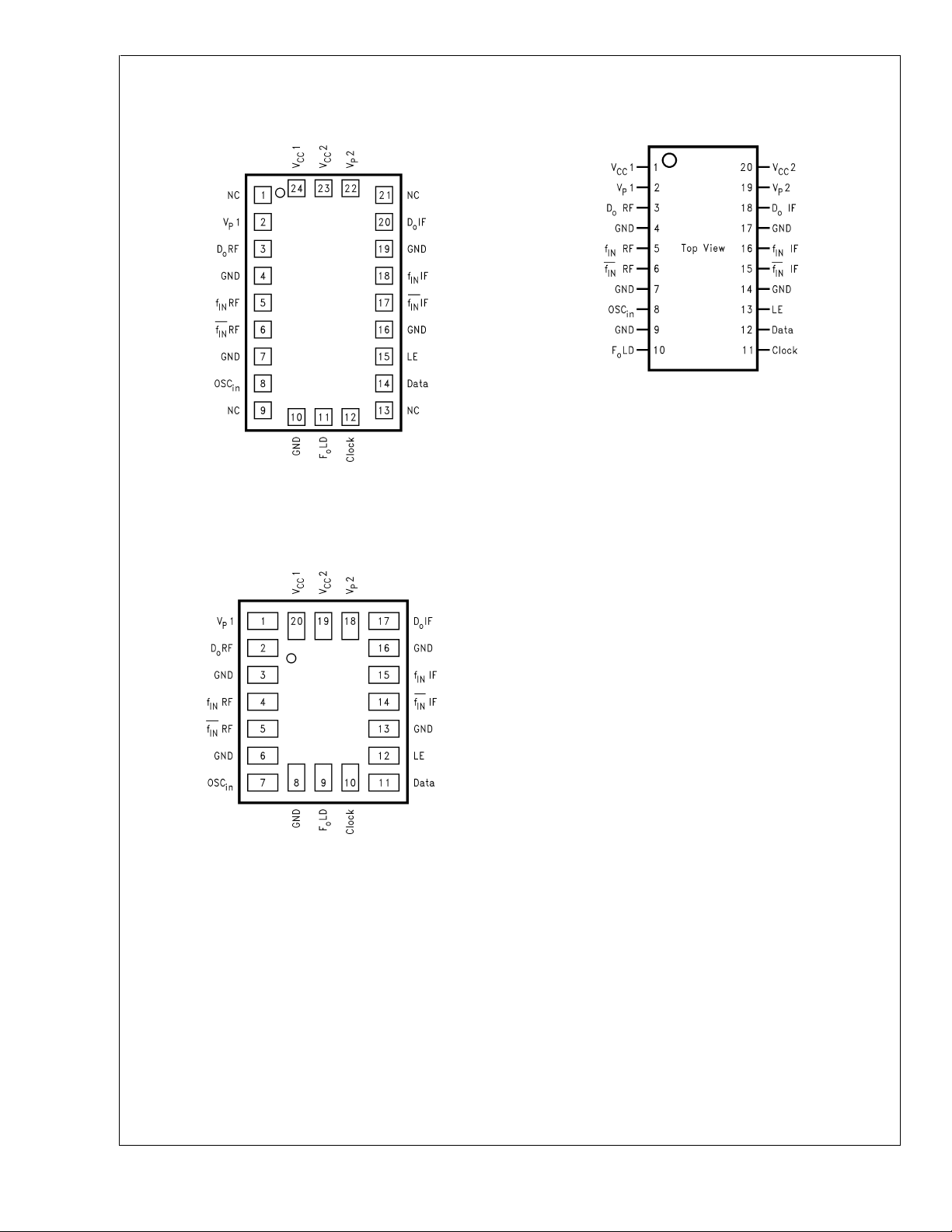
Connection Diagrams
Chip Scale Package (SLB)
(Top View)
LMX2330L/LMX2331L/LMX2332L
Order Number LMX2330LSBX, LMX2331LSLBX or
LMX2332LSLBX
NS Package Number SLB24A
20-Pin Thin Chipscale Package (SLD)
(Top View)
Thin Shrink Small Outline Package (TM)
(Top View)
01280602
Order Number LMX2330LTM, LMX2331LTM or
LMX2332LTM
Order Number LMX2330LTMX, LMX2331LTMX, or
LMX2332LTMX
NS Package Number MTC20
01280639
Order Number LMX2330LSLDX, LMX2331LSLDX, or
01280640
LMX2332LSLDX
NS Package Number SLD20A
www.national.com 2

Pin Descriptions
LMX2330L/LMX2331L/LMX2332L
Pin No.
LMX233XLSLD
20-pin Thin
CSP Package
20 24 1 V
Pin No.
LMX233XLSLB
24-pin CSP
Package
Pin No.
LMX233XLTM
20-pin TSSOP
Package
Pin
Name
CC
I/O Description
1 — Power supply voltage input for RF analog and RF digital circuits.
Input may range from 2.7V to 5.5V. V
1 must equal VCC2.
CC
Bypass capacitors should be placed as close as possible to this
pin and be connected directly to the ground plane.
122V
233D
1 — Power Supply for RF charge pump. Must be ≥ VCC.
P
RF O Internal charge pump output. For connection to a loop filter for
o
driving the input of an external VCO.
3 4 4 GND — Ground for RF digital circuitry.
455f
566f
RF I RF prescaler input. Small signal input from the VCO.
IN
RF I RF prescaler complementary input. A bypass capacitor should
IN
be placed as close as possible to this pin and be connected
directly to the ground plane. Capacitor is optional with some loss
of sensitivity.
6 7 7 GND — Ground for RF analog circuitry.
788OSC
I Oscillator input. The input has a VCC/2 input threshold and can
in
be driven from an external CMOS or TTL logic gate.
8 10 9 GND — Ground for IF digital, MICROWIRE
™
,FoLD, and oscillator
circuits.
91110F
LD O Multiplexed output of the RF/IF programmable or reference
o
dividers, RF/IF lock detect signals and Fastlock mode. CMOS
(see Programmable Modes).
output
10 12 11 Clock I High impedance CMOS Clock input. Data for the various
counters is clocked in on the rising edge, into the 22-bit shift
register.
11 14 12 Data I Binary serial data input. Data entered MSB first. The last two bits
are the control bits. High impedance CMOS input.
12 15 13 LE I Load enable high impedance CMOS input. When LE goes HIGH,
data stored in the shift registers is loaded into one of the 4
appropriate latches (control bit dependent).
13 16 14 GND — Ground for IF analog circuitry.
14 17 15 f
IF I IF prescaler complementary input. A bypass capacitor should be
IN
placed as close as possible to this pin and be connected directly
to the ground plane. Capacitor is optional with some loss of
sensitivity.
15 18 16 f
16 19 17 GND — Ground for IF digital, MICROWIRE, F
17 20 18 D
RF I IF prescaler input. Small signal input from the VCO.
IN
LD, and oscillator circuits.
o
IF O IF charge pump output. For connection to a loop filter for driving
o
the input of an external VCO.
18 22 19 V
19 23 20 V
2 — Power Supply for IF charge pump. Must be ≥ VCC.
P
2 — Power supply voltage input for IF analog, IF digital,
CC
MICROWIRE, F
2.7V to 5.5V. V
LD, and oscillator circuits. Input may range from
o
2 must equal VCC1. Bypass capacitors should
CC
be placed as close as possible to this pin and be connected
directly to the ground plane.
X 1, 9, 13, 21 X NC — No connect.
www.national.com3

Block Diagram
LMX2330L/LMX2331L/LMX2332L
Note: The RF prescaler for the LMX2331L/32L is either 64/65 or 128/129, while the prescaler for the LMX2330L is 32/33 or 64/65.
Note: V
R-counter along with the OSC
Note: V
1 supplies power to the RF prescaler, N-counter, R-counter and phase detector. VCC2 supplies power to the IF prescaler, N-counter, phase detector,
CC
1 and VP2 can be run separately as long as VP≥ VCC.
P
buffer, MICROWIRE, and FoLD. VCC1 and VCC2 are clamped to each other by diodes and must be run at the same voltage level.
in
01280603
www.national.com 4

LMX2330L/LMX2331L/LMX2332L
Absolute Maximum Ratings (Notes 1,
2)
If Military/Aerospace specified devices are required,
please contact the National Semiconductor Sales Office/
Distributors for availability and specifications.
Power Supply Voltage
V
CC
V
P
Voltage on Any Pin
with GND = 0V (V
Storage Temperature Range (T
) −0.3V to VCC+0.3V
I
) −65˚C to +150˚C
S
Lead Temperature (solder 4 sec.)
(T
) +260˚C
L
−0.3V to +6.5V
−0.3V to +6.5V
Recommended Operating Conditions
Power Supply Voltage
V
CC
V
P
Operating Temperature (T
Note 1: Absolute Maximum Ratings indicate limits beyond which damage to
the device may occur. Recommended Operating Conditions indicate conditions for which the device is intended to be functional, but do not guarantee
specific performance limits. For guaranteed specifications and test conditions, see the Electrical Characteristics. The guaranteed specifications apply
only for the test conditions listed.
Note 2: This device is a high performance RF integrated circuit with an ESD
<
2 keV and is ESD sensitive. Handling and assembly of this device
rating
should only be done at ESD protected work stations.
) −40˚C to +85˚C
A
2.7V to 5.5V
VCCto +5.5V
Electrical Characteristics
VCC= 3.0V, VP= 3.0V; −40˚C<T
Symbol Parameter Conditions
I
CC
Power LMX2330L RF + IF VCC= 2.7V to 5.5V 5.0 6.6
Supply LMX2330L RF Only 4.0 5.2
Current LMX2331L RF + IF 4.0 5.4
I
CC-PWDN
f
IN
Powerdown Current (Note 3) 1 10 µA
RF Operating LMX2330L 0.5 2.5
Frequency LMX2331L 0.2 2.0 GHz
f
IF Operating LMX233xL 45 510 MHz
IN
Frequency
f
f
OSC
φ
Oscillator Frequency 5 40 MHz
Maximum Phase Detector 10 MHz
Frequency
Pf
RF RF Input Sensitivity VCC= 3.0V −15 0 dBm
IN
Pf
IF IF Input Sensitivity VCC= 2.7V to 5.5V −10 0 dBm
IN
V
OSC
V
IH
V
IL
I
IH
I
IL
I
IH
I
IL
V
OH
V
OL
t
CS
t
CH
Oscillator Sensitivity OSC
High-Level Input Voltage (Note 4) 0.8 V
Low-Level Input Voltage (Note 4) 0.2 V
High-Level Input Current VIH=VCC= 5.5V (Note
Low-Level Input Current VIL= 0V, VCC= 5.5V
Oscillator Input Current VIH=VCC= 5.5V 100 µA
Oscillator Input Current VIL= 0V, VCC= 5.5V −100 µA
High-Level Output Voltage (for
LD, pin number 10)
F
o
Low-Level Output Voltage (for
LD, pin number 10)
F
o
Data to Clock Set Up Time See Data Input Timing 50 ns
Data to Clock Hold Time See Data Input Timing 10 ns
<
85˚C, except as specified
A
Value
Min Typ Max
LMX2331L RF Only 3.0 4.0 mA
LMX2332L IF + RF 3.0 4.1
LMX2332L RF Only 2.0 2.7
LMX233xL IF Only 1.0 1.4
LMX2332L 0.1 1.2
V
= 5.0V −10 0 dBm
CC
in
0.5 V
CC
−1.0 1.0 µA
4)
−1.0 1.0 µA
(Note 4)
I
= −500 µA VCC− 0.4 V
OH
I
= 500 µA 0.4 V
OL
CC
Units
PP
V
V
www.national.com5

Electrical Characteristics (Continued)
VCC= 3.0V, VP= 3.0V; −40˚C<T
Symbol Parameter Conditions
t
CWH
t
CWL
t
ES
t
EW
Note 3: Clock, Data and LE = GND or Vcc.
Note 4: Clock, Data and LE does not include f
Clock Pulse Width High See Data Input Timing 50 ns
Clock Pulse Width Low See Data Input Timing 50 ns
Clock to Load Enable Set Up Time See Data Input Timing 50 ns
Load Enable Pulse Width See Data Input Timing 50 ns
LMX2330L/LMX2331L/LMX2332L
<
85˚C, except as specified
A
RF, fINIF and OSCIN.
IN
Value
Min Typ Max
Charge Pump Characteristics
VCC= 3.0V, VP= 3.0V; −40˚C<TA≤ 85˚C, except as specified
Symbol Parameter Conditions
I
-SOURCE Charge Pump Output VDo=VP/2, I
Do
I
-SINK Current VDo=VP/2, I
Do
I
-SOURCE VDo=VP/2, I
Do
I
-SINK VDo=VP/2, I
Do
I
-TRI Charge Pump 0.5V ≤ VDo≤ VP− 0.5V −2.5 2.5
Do
<
= 25˚C
A
T
TRI-STATE Current −40˚C
I
-SINK vs CP Sink vs VDo=VP/2 3 10 %
Do
I
SOURCE Source Mismatch (Note 7) TA= 25˚C
Do-
I
vs V
Do
Do
CP Current vs Voltage 0.5 ≤ VDo≤ VP− 0.5V 10 15 %
(Note 6) T
I
vs T
Do
A
CP Current vs VDo=VP/2 10 %
Temperature (Note 8) −40˚C ≤ T
Note 5: See PROGRAMMABLE MODES for I
description.
CPo
= HIGH (Note 5) −4.0 mA
CPo
= HIGH (Note 5) 4.0 mA
CPo
= LOW (Note 5) −1 mA
CPo
= LOW (Note 5) 1 mA
CPo
<
85˚C
A
≤ 85˚C
A
Min Typ Max
Value
Units
Units
nA
www.national.com 6
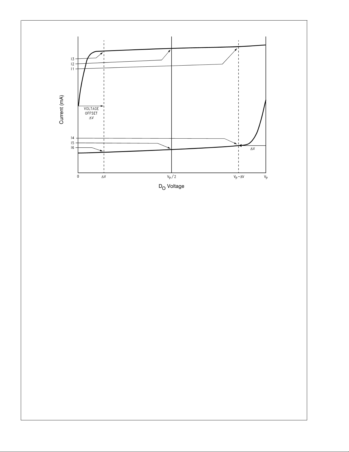
Charge Pump Current Specification Definitions
LMX2330L/LMX2331L/LMX2332L
I1 = CP sink current at VDo=VP−∆V
I2 = CP sink current at V
I3 = CP sink current at V
I4 = CP source current at V
I5 = CP source current at V
I6 = CP source current at V
Do=VP
= ∆V
Do
Do=VP
Do=VP
Do
/2
−∆V
/2
= ∆V
∆V = Voltage offset from positive and negative rails. Dependent on VCO tuning range relative to V
Note 6: I
Note 7: I
Note 8: I
vs VDo= Charge Pump Output Current magnitude variation vs Voltage =
Do
1
*
[
⁄
2
{|I1| − |I3|}]/[1⁄
vs I
Do-sink
[|I2| − |I5|]/[
vs TA= Charge Pump Output Current magnitude variation vs Temperature =
Do
@
[|I2
temp| − |I2@25˚C|]/|I2@25˚C|*100% and [|I5@temp| − |I5@25˚C|]/|I5@25˚C|*100%
*
2
{|I1| + |I3|}]*100% and [1⁄
= Charge Pump Output Current Sink vs Source Mismatch =
Do-source
1
*
⁄
2
{|I2| + |I5|}]*100%
*
2
{|I4| − |I6|}]/[1⁄
*
2
{|I4| + |I6|}]*100%
01280637
and ground. Typical values are between 0.5V and 1.0V.
CC
www.national.com7
 Loading...