NSC LMX2310UEVAL, LMX2310USLDX Datasheet
LMX2310U/LMX2311U/LMX2312U/LMX2313U
PLLatinum
™
Ultra Low Power Frequency Synthesizer for
RF Personal Communications
LMX2310U 2.5 GHz LMX2311U 2.0 GHz
LMX2312U 1.2 GHz LMX2313U 600 MHz
General Description
The LMX2310/1/2/3U are high performance frequency synthesizers. The LMX2310/1/2U use a selectable, dual modulus 32/33 and 16/17 prescaler. The LMX2313U uses a selectable, dual modulus 16/17 and 8/9 prescaler. The device,
when combined with a high quality reference oscillator and a
voltage controlled oscillator, generates very stable, low noise
local oscillator signals for up and down conversion in wireless communication devices.
Serial data is transferred into LMX2310/1/2/3U via a threewire interface (Data, Enable, Clock) that can be directly
interfaced with low voltage baseband processors. Supply
voltage can range from 2.7V to 5.5V. LMX2310U features
very low current consumption, typically 2.3 mA at 3.0V.
The LMX2310/1/2/3U are manufactured using National’s
0.5µ ABiC V silicon BiCMOS process and is available in
20-pin CSP packages.
Features
n RF operation up to 2.5 GHz
n 2.7V to 5.5V operation
n Ultra Low Current Consumption
n Low prescaler values
LMX2310/1/2U 32/33 or 16/17
LMX2313U 16/17 or 8/9
n Excellent Phase Noise
n Internal balanced, low leakage charge pump
n Selectable Charge Pump Current Levels
n Selectable Fastlock mode with Time-Out Counter
n Low Voltage MICROWIRE interface (1.72V to V
CC
)
n Digital and Analog Lock Detect
n Small 20-pad Thin Chip Scale Package
Applications
n Cellular DCS, PCS, WCDMA telephone systems
n Wireless Local Area Networks (WLAN)
n Global Positioning Systems (GPS)
n Other wireless communications systems
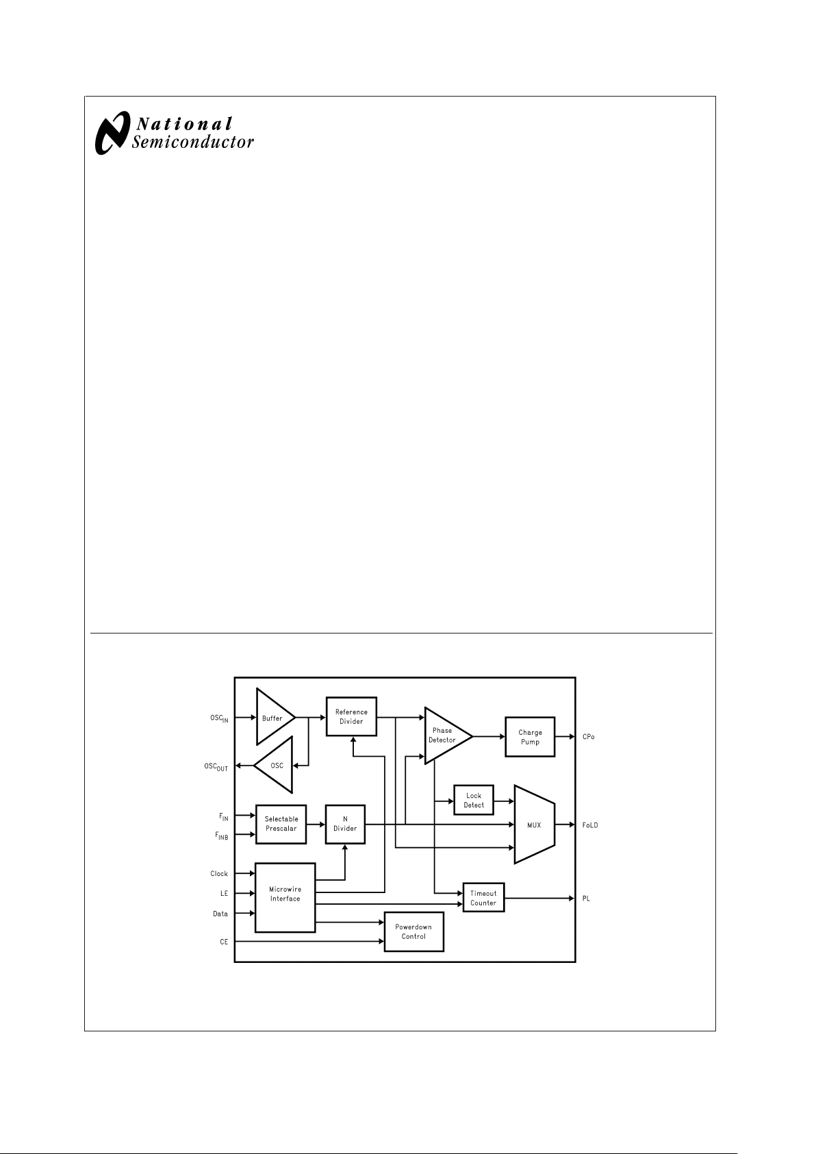
Functional Block Diagram
20043822
PLLatinum™is a trademark of National Semiconductor Corporation.
June 2003
LMX2310U/LMX2311U/LMX2312U/LMX2313U PLLatinum Ultra Low Power Frequency Synthesizer
for RF Personal Communications
© 2003 National Semiconductor Corporation DS200438 www.national.com
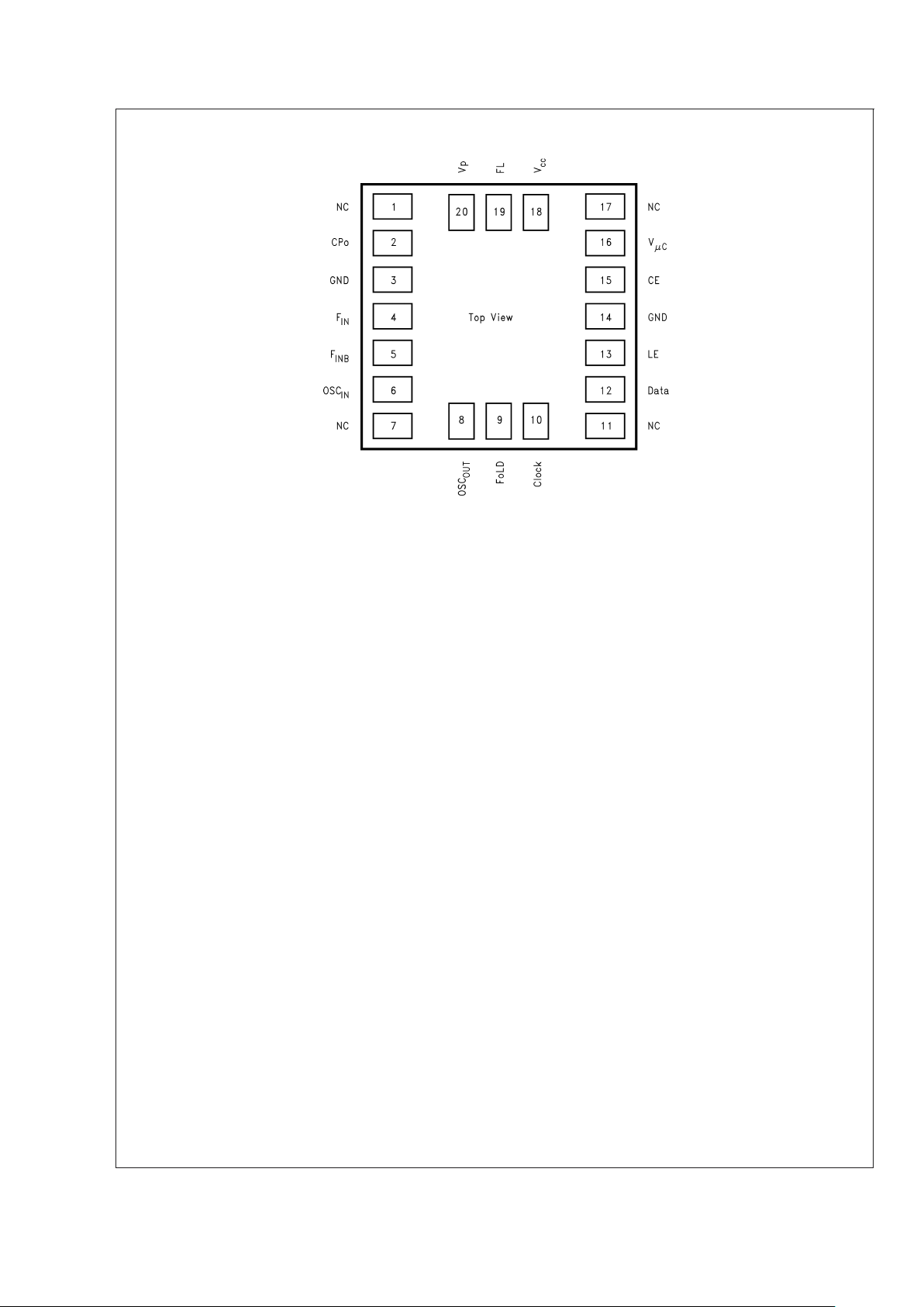
Connection Diagram
20043823
20-Pin Thin Chip Scale Package
NS Package Number SLD20A
LMX2310U/LMX2311U/LMX2312U/LMX2313U
www.national.com 2
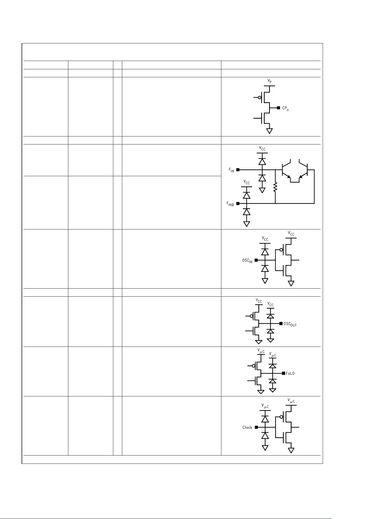
Pin Descriptions
Pin Number Pin Name I/O Description I/O Circuit Configuration
1 NC — No Connect.
2CP
o
O Charge Pump output. For connection to a
loop filter for driving the voltage control
input of an external VCO.
3 GND — Analog ground.
4F
IN
I RF prescaler input. Small signal input
from the VCO.
5F
INB
I RF prescaler complementary input. For
single ended operation, this pin should be
AC grounded. The LMX2310/1/2/3U can
be driven differentially when a bypass
capacitor is omitted.
6 OSC
IN
I Oscillator input. An input to a CMOS low
noise inverting buffer. The input can be
driven from an external CMOS or TTL
logic gate.
7 NC — No Connect.
8 OSC
OUT
O Oscillator output. The OSCINlow noise
buffer drives an independent oscillator
buffer. Its output is connected to the
OSC
OUT
pin. It can be used as a buffer to
provide the reference oscillator frequency
to other circuitry or as a crystal oscillator.
9 FoLD O Multi-function CMOS output pin that
provides multiplexed access to digital lock
detect, open drain analog lock detect, as
well as the outputs of the R and N
counters. The FoLD pin is internally
referenced to V
µC
.
10 Clock I High impedance CMOS Clock input. Data
for the counters is clocked in on the rising
edge, into the 22-bit shift register. The
Clock is internally referenced to V
µC
.
LMX2310U/LMX2311U/LMX2312U/LMX2313U
www.national.com3
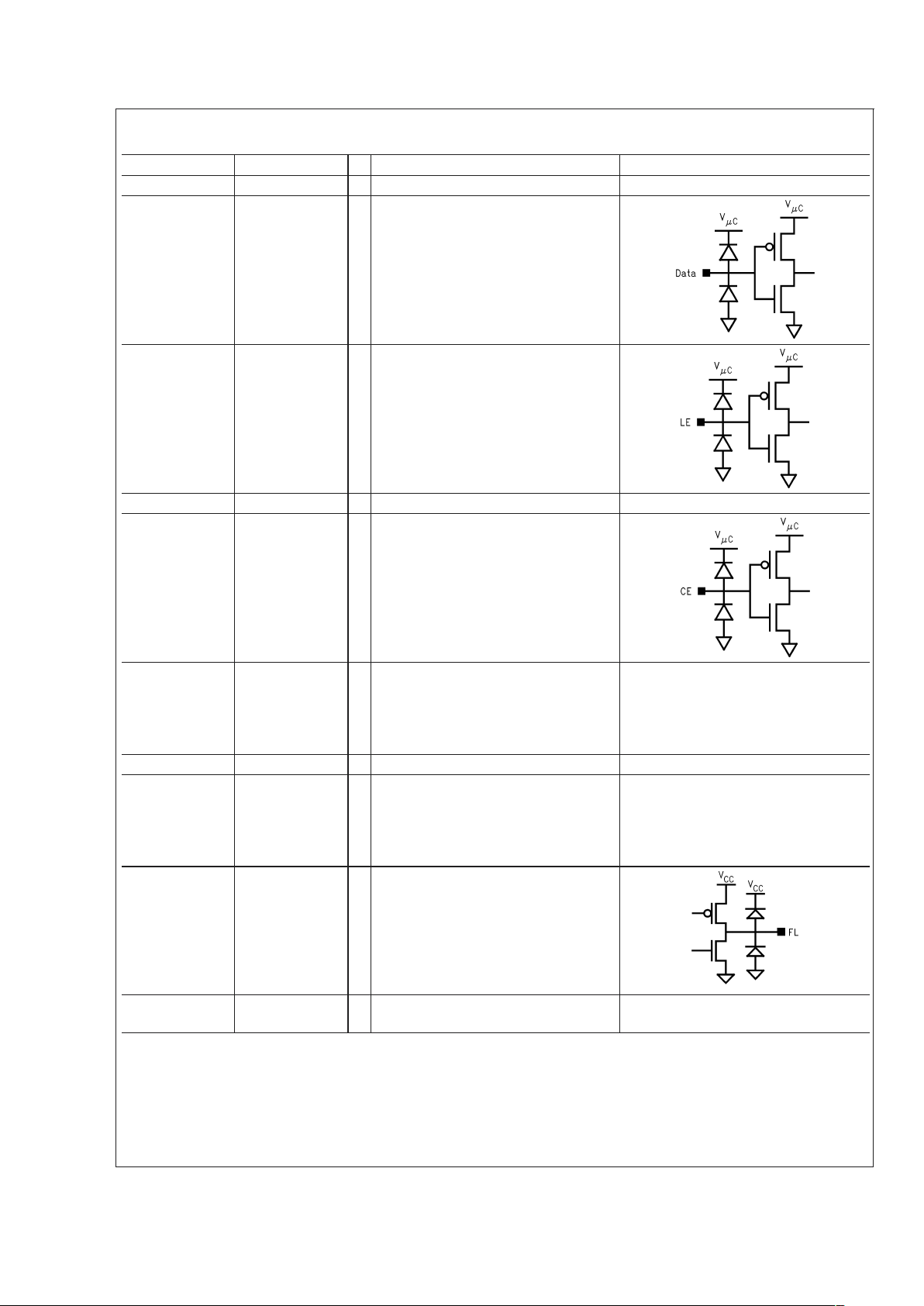
Pin Descriptions (Continued)
Pin Number Pin Name I/O Description I/O Circuit Configuration
11 NC — No Connect.
12 Data I High impedance CMOS Data input. Serial
Data is entered MSB first. The last two
bits are the address for the target
registers. The Data is internally referenced
to V
µC
.
13 LE I High impedance CMOS LE input. When
Latch Enable goes HIGH, data stored in
the 22-bit shift register is loaded into one
the 3 control registers, based on the
address field. The Latch Enable is
internally referenced to V
µC
.
14 GND — Digital ground.
15 CE I High impedance CMOS Chip Enable
input. Provides logical power-down control
of the device. Pull-up to V
µC
if unused.
The Chip Enable is internally referenced
to V
µC
.
16 V
µC
— Power supply for MICROWIRE™circuitry.
Must be ≤ V
CC
. Typically connected to
same supply level as microprocessor or
baseband controller to enable
programming at low voltages.
17 NC — No Connect.
18 V
CC
— Power supply voltage input. Input may
range from 2.7V to 5.5V. Bypass
capacitors should be placed as close as
possible to this pin and be connected
directly to the ground plane.
19 FL O Fastlock mode output. In Fastlock mode
this pin is at logic low. When not in
Fastlock mode, this pin is in TRI-STATE
mode. This pin can also be forced to
TRI-STATE, forced low or forced high by
the programming of the first two-bits of the
Timeout Counter.
20 V
P
— Power supply for charge pump. Must be ≥
V
CC
.
LMX2310U/LMX2311U/LMX2312U/LMX2313U
www.national.com 4
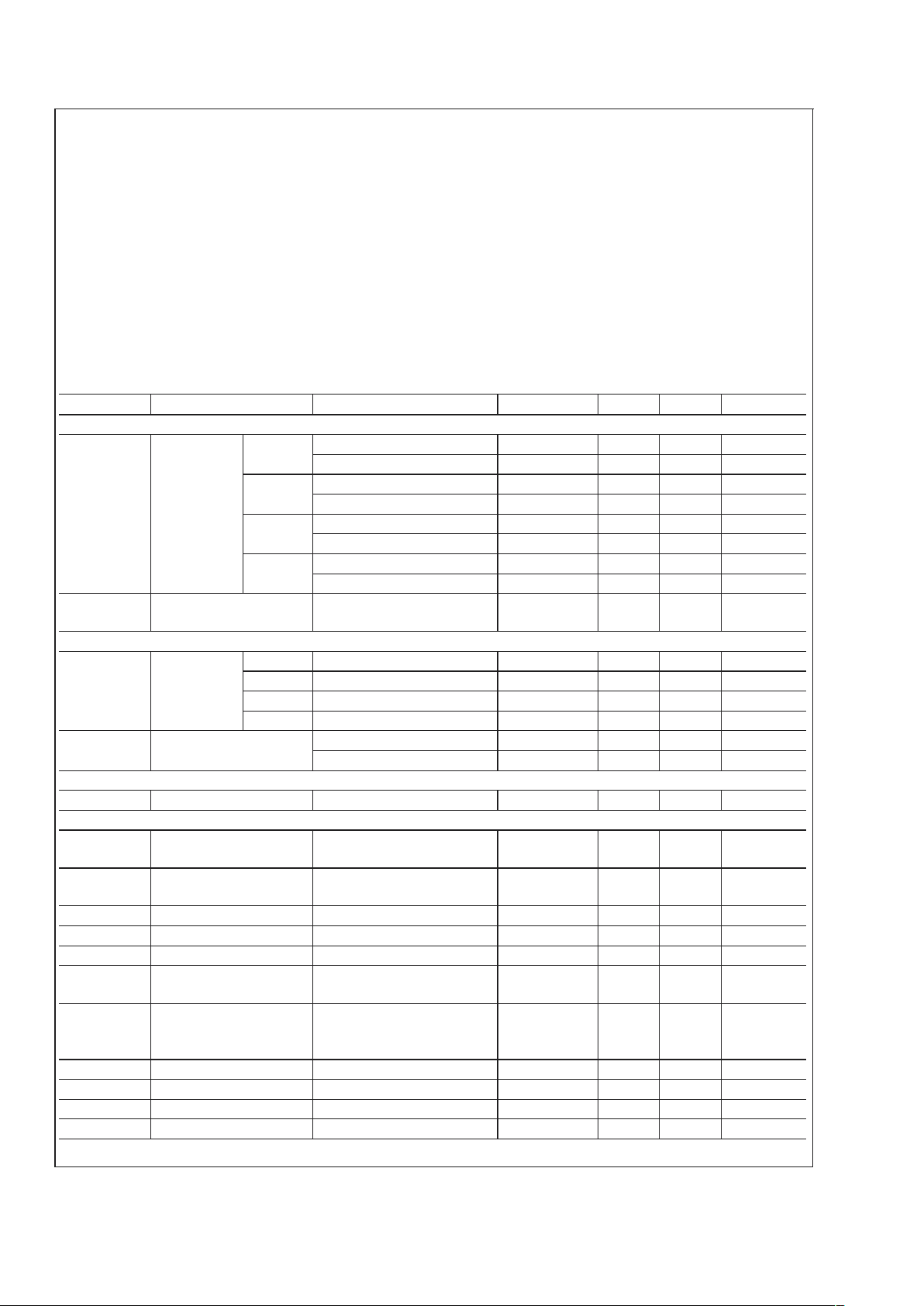
Absolute Maximum Ratings (Notes 1,
2)
If Military/Aerospace specified devices are required,
please contact the National Semiconductor Sales Office/
Distributors for availability and specifications.
Power Supply Voltage,
(V
CC,VP,VµC
) −0.3V to +6.5V
Voltage on any pin with GND=0V
CP
o
, FL, FIN, OSCIN, OSC
OUT(Vi
) −0.3V to VCC+ 0.3V
Data, Clock, LE, CE, FoLD (V
i
) −0.3V to VµC+ 0.3V
Storage Temperature Range, (T
S
) −65˚C to +150˚C
Lead Temp. (solder 4 sec.), (T
L
) +260˚C
Recommended Operating
Conditions
(Note 1)
Min Max Unit
Power Supply Voltage
(V
CC
) 2.7 5.5 V
(V
P
)V
CC
5.5 V
(V
µC
) 1.72 V
CC
V
Operating Temperature, (T
A
) −40 +85 ˚C
Electrical Characteristics
VCC=VP=VµC= 3.0V, −40˚C<T
A
<
+85˚C unless specified otherwise.
Symbol Parameter Conditions (Note 3) Min Typ Max Units
I
CC
l
CC
Power Supply
Current
LMX2310U
2.3 3.0 mA
V
CC
= 5.5V 3.4 mA
LMX2311U
2.0 2.7 mA
V
CC
= 5.5V 3.2 mA
LMX2312U
1.4 2.0 mA
V
CC
= 5.5V 2.4 mA
LMX2313U
1.0 1.3 mA
V
CC
= 5.5V 1.6 mA
I
CC-PWDN
Power-Down Current
Clock, Data and LE = GND
CE = GND
110 µA
RF PRESCALER
F
IN
Operating
Frequency
LMX2310U 0.5 2.5 GHz
LMX2311U 0.5 2.0 GHz
LMX2312U 0.2 1.2 GHz
LMX2313U 45 600 MHz
PF
IN
Input Sensitivity, RF
Prescaler
2.7 ≤ V
CC
≤3.0V (Note 4) −15 0 dBm
3.0V
<
VCC≤ 5.5V (Note 4) −10 0 dBm
PHASE DETECTOR
Fφ Phase Detector Frequency 10 MHz
REFERENCE OSCILLATOR
F
OSC
Operating Frequency,
Reference Oscillator Input
2 50 MHz
V
OSC
IN
Input Sensitivity,
Reference Oscillator Input
(Note 5) 0.5 V
CC
V
P−P
I
IH
OSCINInput Current VIH=VCC= 5.5V 100 µA
I
IL
OSCINInput Current VIL=0,VCC= 5.5V −100 µA
V
OSC
OUT
OSC
OUT
Bias Level OSCINOpen 1.5 V
D
OSC
OUT
OSC
OUT
Duty Cycle
OSC
IN
= 20 MHz, 0.5 V
P-P
,
OSC
IN
Duty Cycle = 50%
50 %
V
OSC
OUT
OSC
OUT
Level
OSC
IN
= 20 MHz, 0.5 V
P-P
,
OSC
OUT
Load=10pF||10k
Ohm
2.6 V
P-P
V
OH
OSC
OUT
Output Voltage IOH= -500 µA 2.6 2.8 V
V
OL
OSC
OUT
Output Voltage IOL= 500 µA 0.2 0.4 V
I
OH
OSC
OUT
Output Current VOH= 2.25 V -1.1 mA
I
OL
OSC
OUT
Output Current VOL= 0.75 V 1.1 mA
LMX2310U/LMX2311U/LMX2312U/LMX2313U
www.national.com5
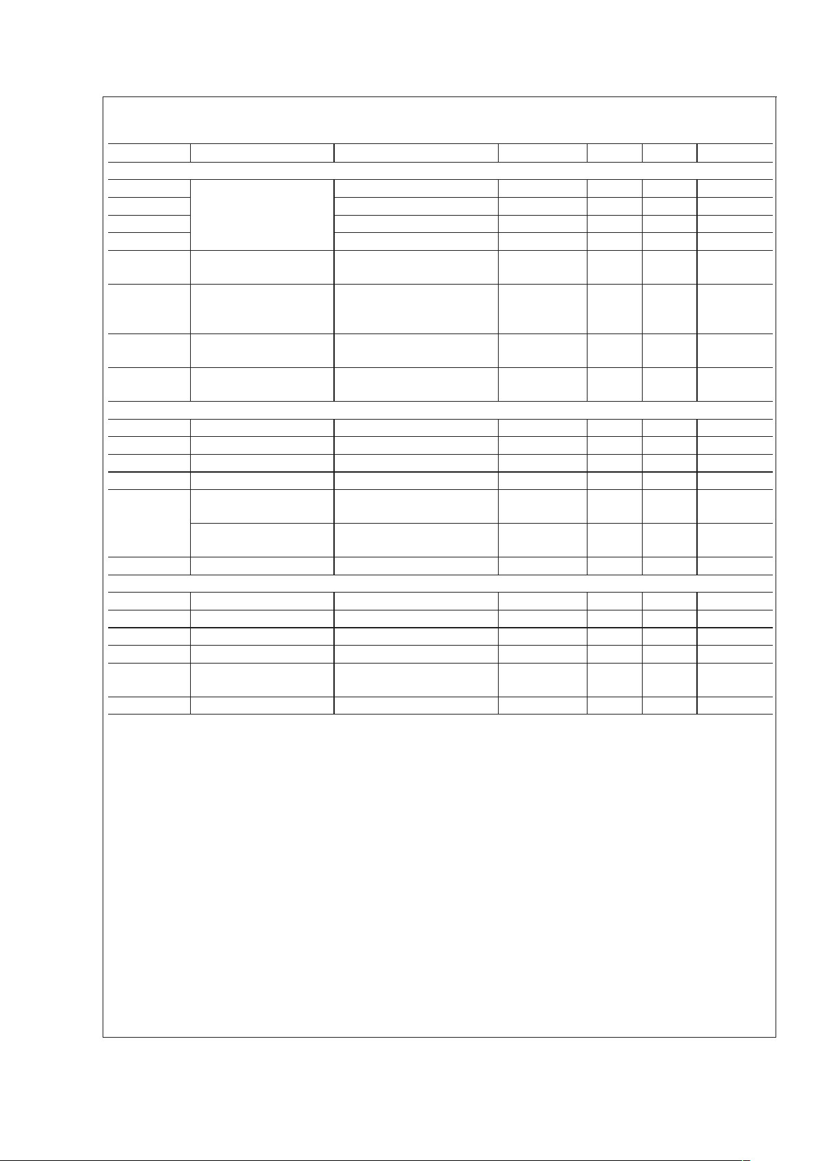
Electrical Characteristics (Continued)
VCC=VP=VµC= 3.0V, −40˚C<T
A
<
+85˚C unless specified otherwise.
Symbol Parameter Conditions (Note 3) Min Typ Max Units
CHARGE PUMP
ICPo-
source
Charge Pump Output
Current (Note 6)
VCPo = Vp/2, ICPo_4X = 0 0.8 1.0 1.2 mA
ICPo-
sink
VCPo = Vp/2, ICPo_4X = 0 −0.8 −1.0 −1.2 mA
ICPo-
source
VCPo = Vp/2, ICPo_4X = 1 3.2 4.0 4.8 mA
ICPo-
sink
VCPo = Vp/2, ICPo_4X = 1 −3.2 −4.0 −4.8 mA
ICPo-
tri
Charge Pump TRI-STATE
Current
0.5V ≤ VCPo ≤ VP− 0.5V
−2.5 2.5 nA
ICPo-
sink
vs.
ICPo-
source
CP Sink vs. Source
Mismatch
VCPo = Vp/2
T
A
= 25˚C
(Note 7)
310 %
ICPo vs VCPo CP Current vs. Voltage 0.5V ≤ VCPo ≤ V
P
− 0.5V
T
A
= 25˚C (Note 7)
815 %
ICPo vs T
A
CP Current vs.
Temperature
VCPo = Vp/2V (Note 6)
8%
DIGITAL INTERFACE (Data, Clock, LE, CE)
V
IH
High-level Input Voltage VµC= 1.72V to 5.5V 0.8 V
µC
V
V
IL
Low-level Input Voltage VµC= 1.72V to 5.5V 0.2 V
µC
V
I
IH
High-level Input Current VIH=VµC= 5.5V −1.0 1.0 µA
I
IL
Low-level Input Current VIL= 0V, VµC= 5.5V −1.0 1.0 µA
V
OH
High-level Output Voltage
(Pin 7– FoLD)
IOH= 500 µA
V
µC
− 0.4 V
High-level Output Voltage
(Pin 15– FL)
I
OH
= −500 µA
V
CC
− 0.4 V
V
OL
Low-level Output Voltage IOL= 1.0 mA (Note 8) 0.1 0.4 V
MICROWIRE TIMING (Data, Clock, LE, CE)
t
CS
Data to Clock Set Up Time (Note 9) 50 ns
t
CH
Data to Clock Hold Time (Note 9) 20 ns
t
CWH
Clock Pulse Width High (Note 9) 50 ns
t
CWL
Clock Pulse Width Low (Note 9) 50 ns
t
ES
Clock to Load Enable Set
Up Time
(Note 9)
50 ns
t
EW
Load Enable Pulse Width (Note 9) 50 ns
LMX2310U/LMX2311U/LMX2312U/LMX2313U
www.national.com 6

Electrical Characteristics (Continued)
VCC=VP=VµC= 3.0V, −40˚C<T
A
<
+85˚C unless specified otherwise.
Symbol Parameter Conditions (Note 3) Min Typ Max Units
PHASE NOISE CHARACTERISTICS
L
N
(f)
Normalized Single
Side-Band Phase Noise
F
φ
= 200 kHz
F
OSC
= 10 MHz
V
OSC
= 1.0 V
PP
ICPO=4mA
T
A
= 25˚C
(Note 10)
−159 dBc/Hz
L(f)
Single Side-Band Phase
Noise
LMX2310U
F
IN
= 2450 MHz
F
φ
= 200 kHz
F
OSC
= 10 MHz
V
OSC
= 1.0 V
PP
ICPO=4mA
T
A
= 25˚C
(Note 11)
−78 dBc/Hz
LMX2311U
F
IN
= 1960 MHz
F
φ
= 200 kHz
F
OSC
= 10 MHz
V
OSC
= 1.0 V
PP
ICPO=4mA
T
A
= 25˚C
(Note 11)
−80 dBc/Hz
LMX2312U
F
IN
= 902 MHz
F
φ
= 200 kHz
F
OSC
= 10 MHz
V
OSC
= 1.0 V
PP
ICPO=4mA
T
A
= 25˚C
(Note 11)
−85 dBc/Hz
LMX2313U
F
IN
= 450 MHz
F
φ
= 50 kHz
F
OSC
= 10 MHz
V
OSC
= 1.0 V
PP
ICPO=4mA
T
A
= 25˚C
(Note 11)
−85 dBc/Hz
Note 1: Absolute Maximum Ratings indicate limits beyond which damage to the device may occur. Operating Ratings indicate conditions for which the device is
intended to be functional, but do not guarantee specific performance limits. For guaranteed specifications and conditions, see the Electrical Characteristics. The
guaranteed specifications apply only for the conditions listed.
Note 2: This device is a high performance RF integrated circuit with an ESD rating
<
2 kV. Handling and assembly of this device should only be done at ESD free
workstations.
Note 3: Typical Conditions are at a T
A
of 25˚C.
Note 4: See F
IN
Sensitivity Test Setup.
Note 5: See OSC
IN
Sensitivity Test Setup.
Note 6: Charge Pump Magnitude is controlled by CPo_4X bit [R18].
Note 7: See Charge Pump Measurement Definition for detail on how these measurements are made.
Note 8: Analog Lock Detect open drain output pin only can be pulled up to V
ext
that will not exceed 6.5V.
Note 9: See Serial Input Data Timing.
Note 10: Normalized Single-Side Band Phase Noise is defined as: L
N
(f) = L(f) − 20 log (FIN/Fφ), where L(f) is defined as the Single Side-Band Phase Noise.
Note 11: Phase Noise is measured using a reference evaluation board with a loop bandwidth of approximately 12 kHz. The phase noise specification is the
composite average of 3 measurements made at frequency offsets of 2.0 kHz, 2.5 kHz and 3.0 kHz.
LMX2310U/LMX2311U/LMX2312U/LMX2313U
www.national.com7
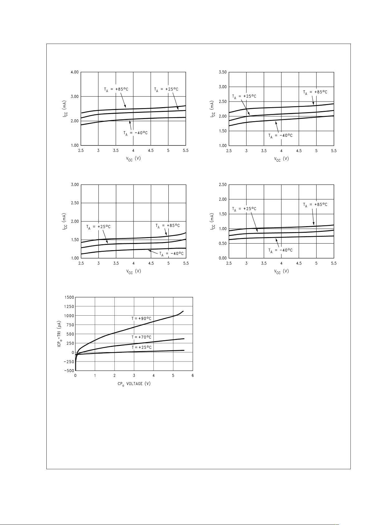
Typical Performance Characteristics
Iccvs VccLMX2310U Iccvs VccLMX2311U
20043838
20043839
Iccvs VccLMX2312U Iccvs VccLMX2313U
20043840 20043841
CPOTRI-STATE vs CPOVoltage
20043843
LMX2310U/LMX2311U/LMX2312U/LMX2313U
www.national.com 8
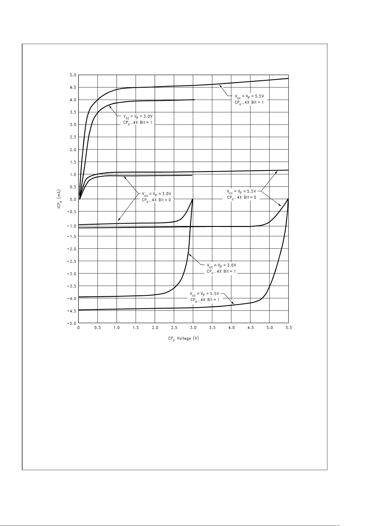
Typical Performance Characteristics (Continued)
LMX231xU Charge Pump Sweeps
20043842
LMX2310U/LMX2311U/LMX2312U/LMX2313U
www.national.com9
 Loading...