NSC LMX2240M Datasheet

LMX2240
Intermediate Frequency Receiver
LMX2240 Intermediate Frequency Receiver
April 1995
General Description
The LMX2240 is a monolithic, integrated intermediate frequency receiver suitable for use in Digital European Cordless Telecommunications (DECT) systems as well as other
mobile telephony and wireless communications applications. It is fabricated using National’s ABiC
process (f
T
e
15 GHz).
TM
IV BiCMOS
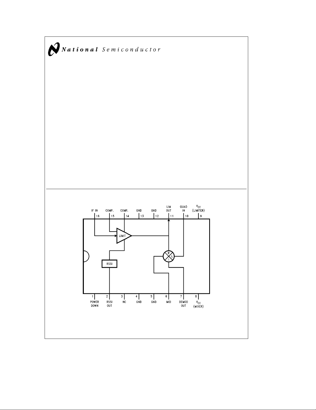
The LMX2240 consists of a high gain limiting amplifier, a
frequency discriminator, and a received signal strength indicator (RSSI). The high gain limiting amplifier and discriminator operate in the 40 MHz to 150 MHz frequency range, and
the limiter has approximately 70 dB of gain. The use of the
limiter and the discriminator provides a low cost, high performance demodulator for communications systems. The
RSSI output can be used for channel quality monitoring.
The LMX2240 is intended to support single conversion receivers. This device saves power, size, and cost by eliminating the second local oscillator (LO), second converter (mixer), and additional filters. The LMX2240 is recommended for
systems with channel bandwidths of 300 kHz to 2.5 MHz.
The LMX2240 is available in a 16-pin JEDEC surface mount
plastic package.
Functional Block Diagram
Features
Y
Typical operation at 110 MHz
Y
RF sensitivity tob75 dBm; RSSI sensitivity to
b
82 dBm
Y
High gain (70 dB) limiting amplifier
Y
Average current consumption: 480 mA for DECT
handset (burst mode)
Y
a
3V operation
Y
Power down mode for increased current savings
Y
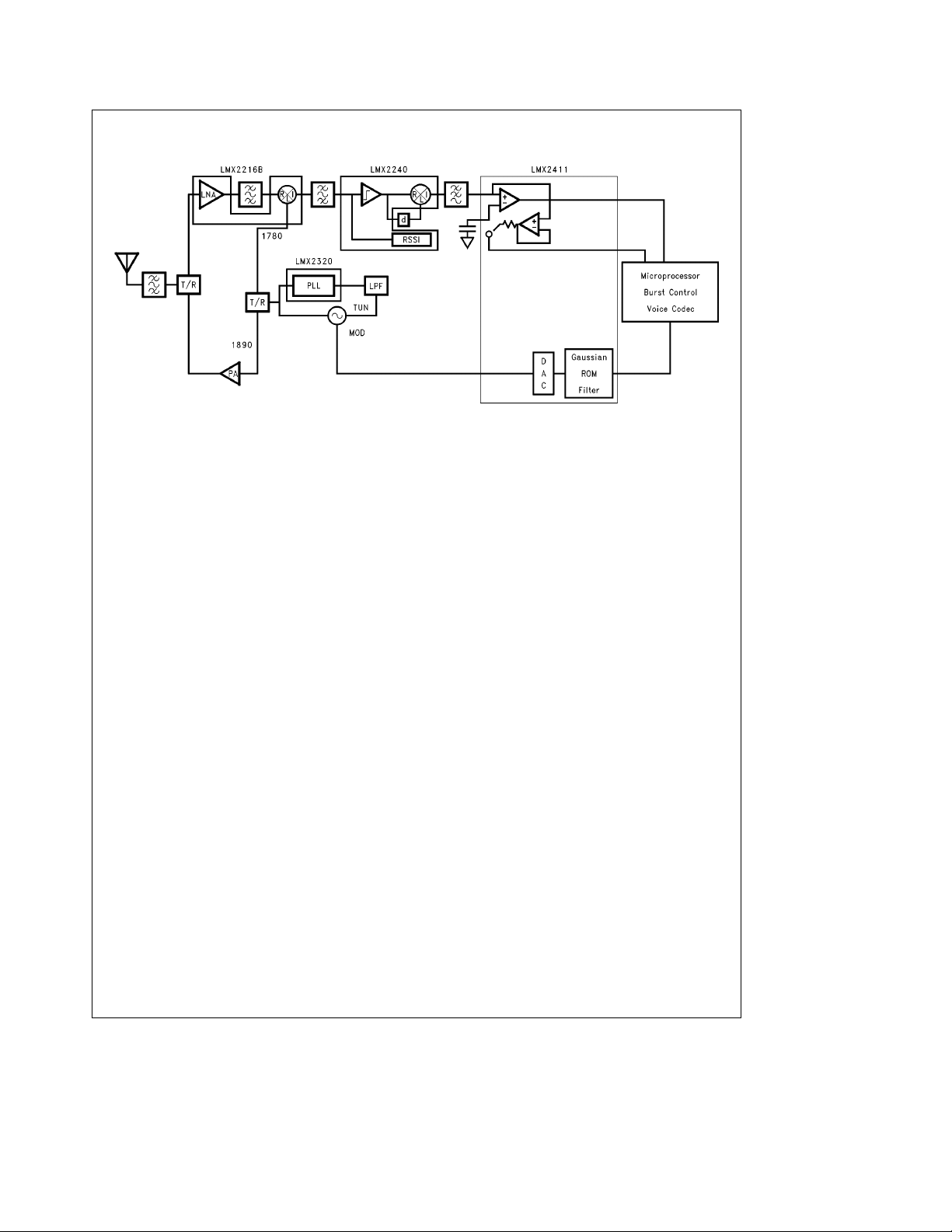
Part of a complete receiver solution with the LMX2216
LNA/Mixer, the LMX2315/20 Phase-locked Loop, and
the LMX2411 Baseband Processor
Y
Compliant to ARi
1
TM
specification
Applications
Y
Digital European Cordless Telecommunications (DECT)
Y
Portable wireless communications (PCS/PCN, cordless)
Y
Wireless local area networks (WLANs)
Y
Digital cellular telephone systems
Y
Other wireless communications systems
TL/W/11755– 1
1
ABiCTMand ARi
C
1995 National Semiconductor Corporation RRD-B30M115/Printed in U. S. A.
TM
are trademarks of National Semiconductor Corporation.
TL/W/11755

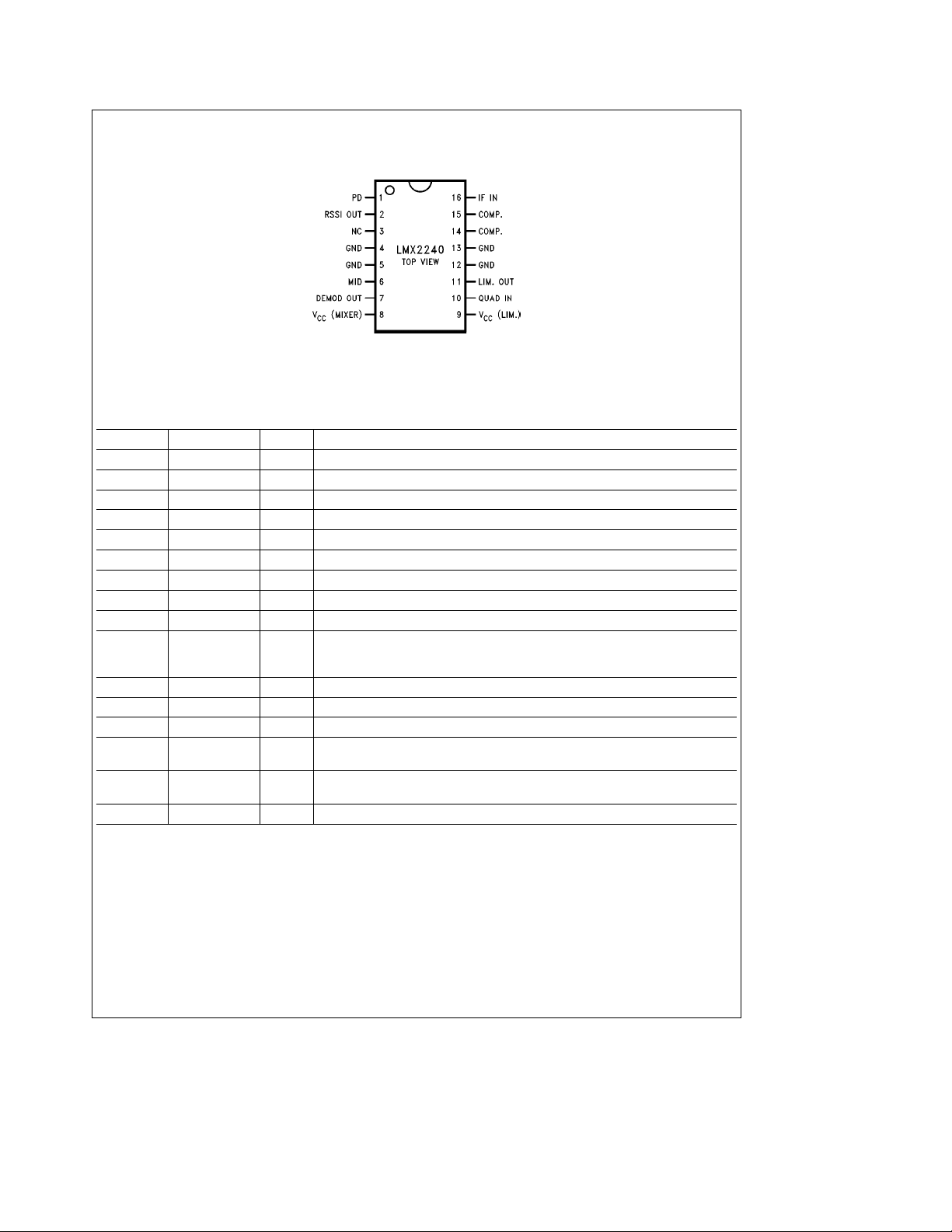
Connection Diagram
Small Outline Package
TL/W/11755– 2
Top View
Order Number LMX2240M
See NS Package Number M16A
Pin Description
Pin No. Pin Name I/O Description
1 PD I Power Down; a HIGH signal switches the part to power down mode.
2 RSSI Out O Voltage output of the received signal strength indicator (RSSI).
3 NC No connection
4 GND Ground
5 GND Ground
6 MID O Mid-range output of the discriminator; can be used for comparator threshold.
7 Demod Out O Demodulated output of the discriminator.
8V
9V
10 Quad In I Quadrature input. A DC path from source through an inductor must be present at
11 Lim. Out O Limiter output to the quadrature tank.
12 GND Ground
13 GND Ground
14 Comp. Compensation pin for the limiter. See Applications Information for capacitor
15 Comp. Compensation pin for the limiter. See Applications Information for capacitor
16 IF In I IF input to the limiter.
(Mixer) Source voltage for the mixer (discriminator).
CC
(Lim.) Source voltage for the limiter.
CC
this pin, but, there must be no series resistance (a parallel resistor to the inductor
is acceptable).
value.
value.
2

Absolute Maximum Ratings
If Military/Aerospace specified devices are required,
please contact the National Semiconductor Sales
Office/Distributors for availability and specifications.
Power Supply Voltage (V
Storage Temperature Range (TS)
Lead Temperature (T
(Soldering, 10 seconds)
) 6.5V
CC
)
L
b
65§Ctoa150§C
a
260§C
Recommended Operating
Conditions
Supply Voltage (V
3V 2.85 3.15 V
CC
)
Operating Temperature (T
Min Max Units
b
)
A
10
a
70
C
§
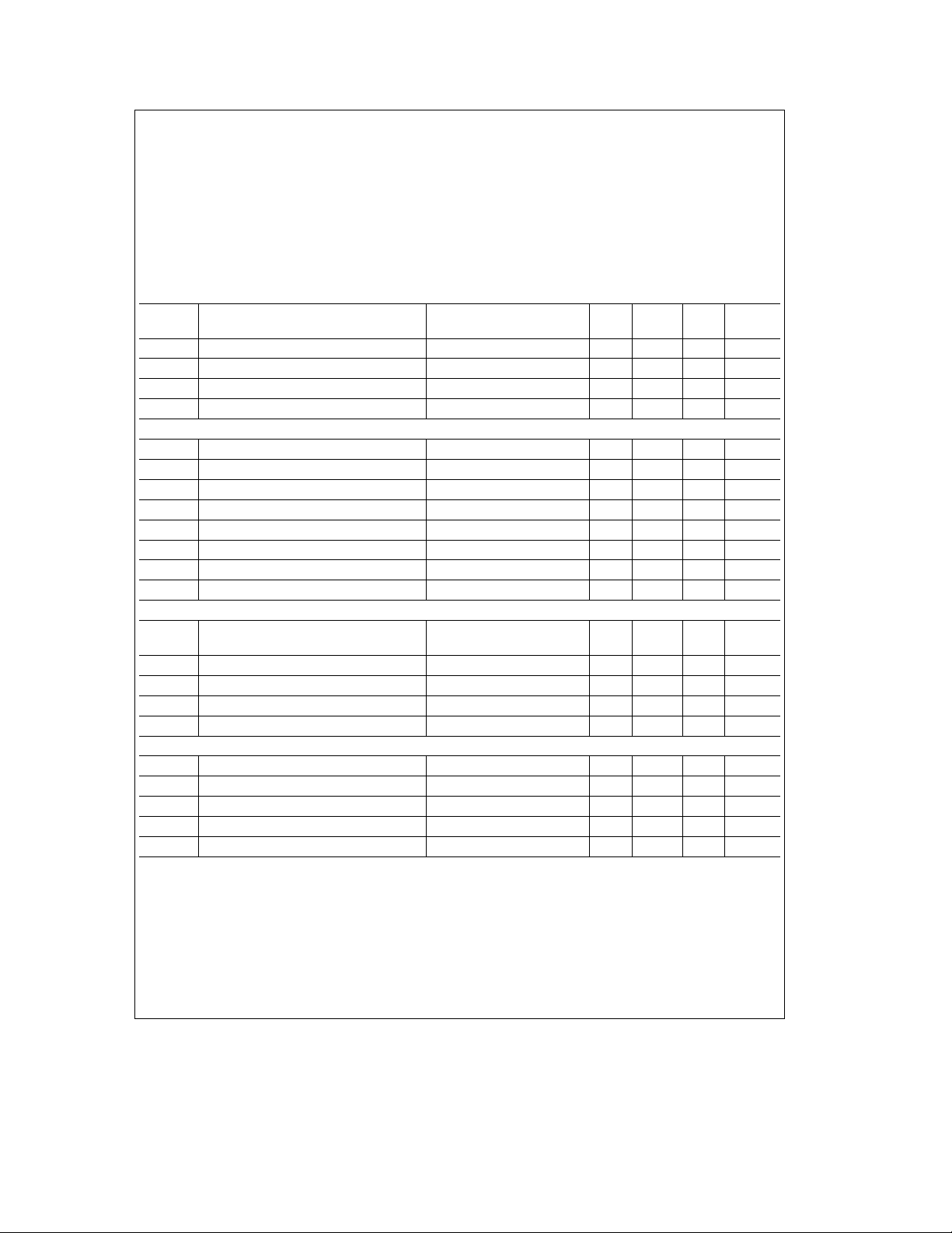
Electrical Characteristics
The following specifications apply for supply voltage V
specified
Symbol Parameter Conditions Min
I
DD
Supply Current 810mA
CC
ea
3Vg5%, f
e
120 MHz, and T
IN
e
25§C unless otherwise
A
Value
Typ
Max Units
IPDPower Down Current 115 200 mA
f
f
max
min
Maximum IF Input Frequency 120 150 MHz
Minimum IF Input Frequency 10 MHz
IF LIMITER
NF IF Limiter Noise Figure 11.5 12.5 dB
A
V
Limiter Gain Z
sens Limiter/Disc. Sensitivity BERe0.001
IF
in
IF
out
V
max
V
out
IF Limiter Input Impedance 150 225 X
IF Limiter Output Impedance 250 X
Maximum Input Voltage Level 500 mV
Output Swing 350 500 V
Lim Input Limiting Point
e
1000X 70 dB
L
b
75 dBm
b
70 dBm
DISCRIMINATOR
V
out
V
OS
Discriminator Output Peak-to-Peak Voltage See Test Circuit 1.0 1.2 V
(Note 1)
Disc. Output DC Voltage (Pin 7) 1.4 1.7 V
MID Mid-Range Output (Pin 6) 1.4 1.7 V
DISC
DISC
Disc. Input Impedance 1000 X
in
Disc. Output Impedance 150 X
out
RSSI
RSSI RSSI Dynamic Range 70 dB
RSSI
RSSI Output Voltage Pineb80 dBm 0.35 0.5 0.8 V
out
Pine0 dBm 1.15 1.5 1.8 V
RSSI Slope Pineb70 dBm tob20 dBm 11 16 mV/dB
RSSI Linearity 3dB
Note 1: The discriminator output peak-to-peak voltage is measured by operating the discriminator mixer with two separate inputs (i.e., as a mixer). A beat frequency
of 1 kHz is generated, and this tone’s output swing is guaranteed to be at least 1.0 V
circuit, the guaranteed 1.0 V
interest from the tank circuit.
output translates to (1.0V *(36/180)e) 200 mVPPdemodulated output, assuming at least 36§phase shift across the band of
PP
. When the mixer is configured as a discriminator with the limiter and a tank
PP
PP
PP
PP
3

Typical Application Block Diagram
Functional Description
OVERVIEW
The LMX2240 IF demodulator is a low power IF processor
that includes a frequency discriminator, an IF hard limiting
amplifier, and a received signal strength indicator (RSSI).
The LMX2240 is capable of differentially demodulating an
FM or AM signal with as high an IF as 150 MHz, avoiding a
costly second down-conversion. The RSSI output can be
used for time gated channel measurements required in
TDMA and other systems. Other features include high receiver sensitivity and a power down mode to allow for standby operation.
THE LIMITING AMPLIFIER
The limiting amplifier has a typical gain of 70 dB and a sensitivity of about
DECT system with 20 dB net RF gain in front of it to achieve
a sensitivity of
with internal compensation at each stage to ensure stability.
Two external compensation capacitors are also required to
further enhance stability. The input to the limiter is a relatively low impedance to allow easy matching to typical IF surface acoustic wave (SAW) filters. The output of the limiter is
connected off chip to an external quadrature tank circuit as
well as connected internally to the discriminator (mixer). The
output impedance of the limiter is 250X (typical).
b
75 dBm. This allows it to be used in the
b
95 dBm. The limiter is a five stage amplifier
TL/W/11755– 3
THE RECEIVED SIGNAL STRENGTH INDICATOR (RSSI)
The RSSI circuit has a range of 70 dB. Its output voltage is
proportional to the logarithm of the input signal level. The
RSSI circuit has a sensitivity of
age of the circuit ranges from 0.5V to 1.5V typically.
THE FREQUENCY DISCRIMINATOR
The frequency discriminator is a Gilbert cell mixer that requires an external tank circuit to create a 90
the desired frequency. The output of this circuit is centered
at 1.5V by an internal level shifting circuit, and a mid-range
voltage (at 1.5V) is also provided. The sensitivity of the discriminator to phase inaccuracies is 5.5 mV/degree (see Applications Information). This means that for a phase imbalance of 10
about 55 mV off of the 1.5V mid-range voltage. For the typical case, this amounts to about 10% of the output eye diagram (for 400 mV
, the received eye diagram will be shifted by
§
output).
PP
b
82 dBm. The output volt-
phase shift at
§
4
 Loading...