NSC LMX2216M Datasheet

LMX2216
0.1 GHz to 2.0 GHz Low Noise Amplifier/Mixer
for RF Personal Communications
General Description
The LMX2216 is a monolithic, integrated low noise amplifier
(LNA) and mixer suitable as a first stage amplifier and downconverter for RF receiver applications. The wideband operating capabilities of the LMX2216 allow it to function over
frequencies from 0.1 GHz to 2.0 GHz. It is fabricated using
National Semiconductor’s ABiC IV BiCMOS process.
All input and output ports of the LMX2216 are single-ended.
The LNA input and output ports are designed to interface to
a50Xsystem. The Mixer input ports are matched to 50X.
The output port is matched to 200X. The only external components required are DC blocking capacitors. The balanced
architecture of the LMX2216 maintains consistent operating
parameters from unit to unit, since it is implemented in a
monolithic device. This consistency provides manufacturers
a significant advantage since tuning proceduresÐoften
needed with discrete designsÐcan be reduced or eliminated.
The low noise amplifier produces very flat gain over the entire operating range. The doubly-balanced, Gilbert-cell mixer
provides good LO-RF isolation and cancellation of secondorder distortion products. A power down feature is implemented on the LMX2216 that is especially useful for standby operation common in Time Division Multiple Access
(TDMA) and Time Division Duplex (TDD) systems.
The LMX2216 is available in a narrow-body 16-pin surface
mount plastic package.
Features
Y
Wideband RF operation from 0.1 GHz to 2.0 GHz
Y
No external biasing components necessary
Y
3V operation
Y
LNA input and output ports matched to 50X
Y
Mixer input ports matched to 50X, output port matched
to 200X.
Y
Doubly balanced Gilbert cell mixer (single ended input
and output)
Y
Low power consumption
Y
Power down feature
Y
Small outline, plastic surface mount package
Applications
Y
Digital European Cordless Telecommunications (DECT)
Y
Portable wireless communications (PCS/PCN, cordless)
Y
Wireless local area networks (WLANs)
Y
Digital cellular telephone systems
Y
Other wireless communications systems
LMX2216 0.1 GHz to 2.0 GHz Low Noise Amplifier/Mixer for RF Personal Communications
August 1995
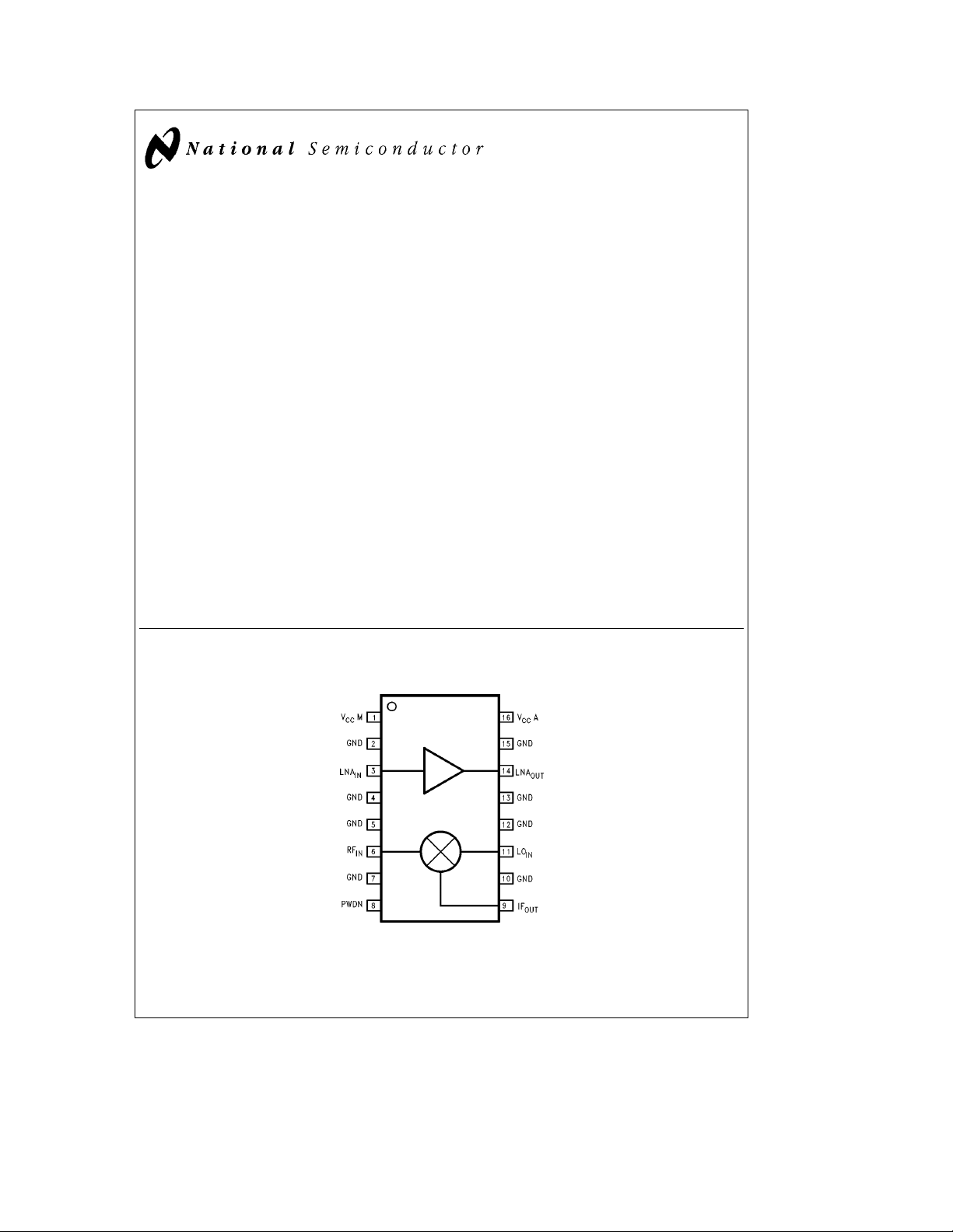
Functional Block/Pin Diagram
Order Number LMX2216M
See NS Package Number M16A
C
1995 National Semiconductor Corporation RRD-B30M115/Printed in U. S. A.
TL/W/11814
TL/W/11814– 1

Pin Description
Pin Pin
No. Name
1VCCM I Voltage supply for the mixer. The input voltage level to this pin should be a DC Voltage ranging from
2 GND Ground
3 LNA
4 GND Ground
5 GND Ground
6RFINI RF input to the mixer. The RF signal to be down converted is connected to this pin. External DC
7 GND Ground
8 PWDN I Power down signal pin. Both the LNA and mixer are powered down when a HIGH level is applied to
9IF
OUT
10 GND Ground
11 LO
12 GND Ground
13 GND Ground
14 LNA
15 GND Ground
16 VCCA I LNA supply Voltage. DC Voltage ranging from 2.85V to 3.15V.
I/O Description
2.85V to 3.15V.
IN
IN
OUT
I RF input signal to the LNA. External DC blocking capacitor is required.
blocking capacitor is required.
this pin (VIH).
O IF output signal of the mixer. External DC blocking capacitor is required.
I Local oscillator input signal to the mixer. External DC blocking capacitor is required.
O Output of the LNA. This pin outputs the amplified RF signal. External DC blocking capacitor is
required.
Absolute Maximum Ratings
If Military/Aerospace specified devices are required,
please contact the National Semiconductor Sales
Office/Distributors for availability and specifications.
Supply Voltage (V
Storage Temperature (T
Operating Temperature (TO)
) 6.5V
CC
)
S
b
65§Ctoa150§C
b
40§Ctoa85§C
Recommended Operating
Conditions
Supply Voltage (VCC) 2.85V–3.15V
Operating Temperature (T
RF
IN
LO
IN
2
)
A
b
10§Ctoa70§C
0.1 GHz to 2.0 GHz
0.1 GHz to 2.0 GHz

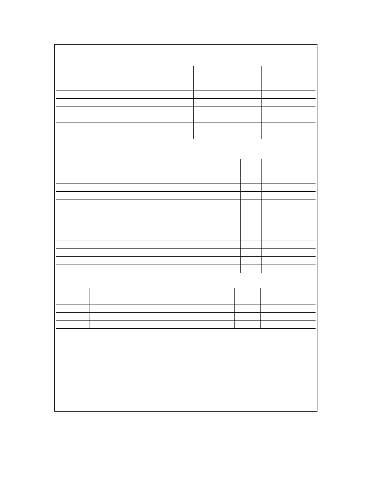
Electrical Characteristics: LNA
ea
(V
CC
3.0Vg5%, T
e
A
25§C, Z
e
o
50X and f
e
IN
Symbol Parameter Conditions Min Typ Max Units
I
CC
I
CC-PWDN
Supply Current In Operation 6.5 8.0 mA
Supply Current In Power Down Mode 10 mA
G Gain 910 dB
P
1dB
Output 1 dB Compression Point
OIP3 Output 3rd Order Intercept Point 5.0 7.0 dBm
NF Single Side Band Noise Figure 4.8 6.0 dB
RL
RL
IN
OUT
Input Return Loss 10 15 dB
Output Return Loss 10 11 dB
2.0 GHz
@
b
30 dBm unless otherwise specified.)
b
5.0b3.0 dBm
Electrical Characteristics: Mixer (V
b
30 dBm, f
e
1.89 GHz@0 dBm; f
LO
e
110 MHz unless otherwise specified.)
IF
CC
ea
3.0Vg5%, T
e
25§C, Z
A
e
50X,f
o
e
2.0 GHz
RF
Symbol Parameter Conditions Min Typ Max Units
I
CC
I
CC-PWDN
G
C
P
1dB
OIP3 Output Third Order Intercept Point
Supply Current In Operation 9.0 12.0 mA
Supply Current In Power Down Mode 10 mA
Conversion Gain (Single Side Band) 4.0 6.0 dB
Output 1 dB Compression Point
b
b
b
13.0
9.0 dBm
3.0 0.0 dBm
SSB NF Single Side Band Noise Figure 17 18 dB
DSB NF Double Side Band Noise Figure 14 15 dB
LO-RF LO to RF Isolation 20 30 dB
LO-IF LO to IF Isolation 20 30 dB
RF RL RF Return Loss 10 15 dB
LO RL LO Return Loss 10 15 dB
IF RL IF Return Loss 15 dB
Z
IF
IF Port Impedance 200 X
Electrical Characteristics: Power Down
Symbol Parameter Conditions Min Typ Max Units
V
IH
V
IL
I
IH
I
IL
High Level Input Voltage V
Low Level Input Voltage 0.8 V
High Level Input Current V
Low Level Input Current V
e
V
IH
CC
e
GND
IL
b
0.8 V
CC
b
10.0 10.0 mA
b
10.0 10.0 mA
@
3

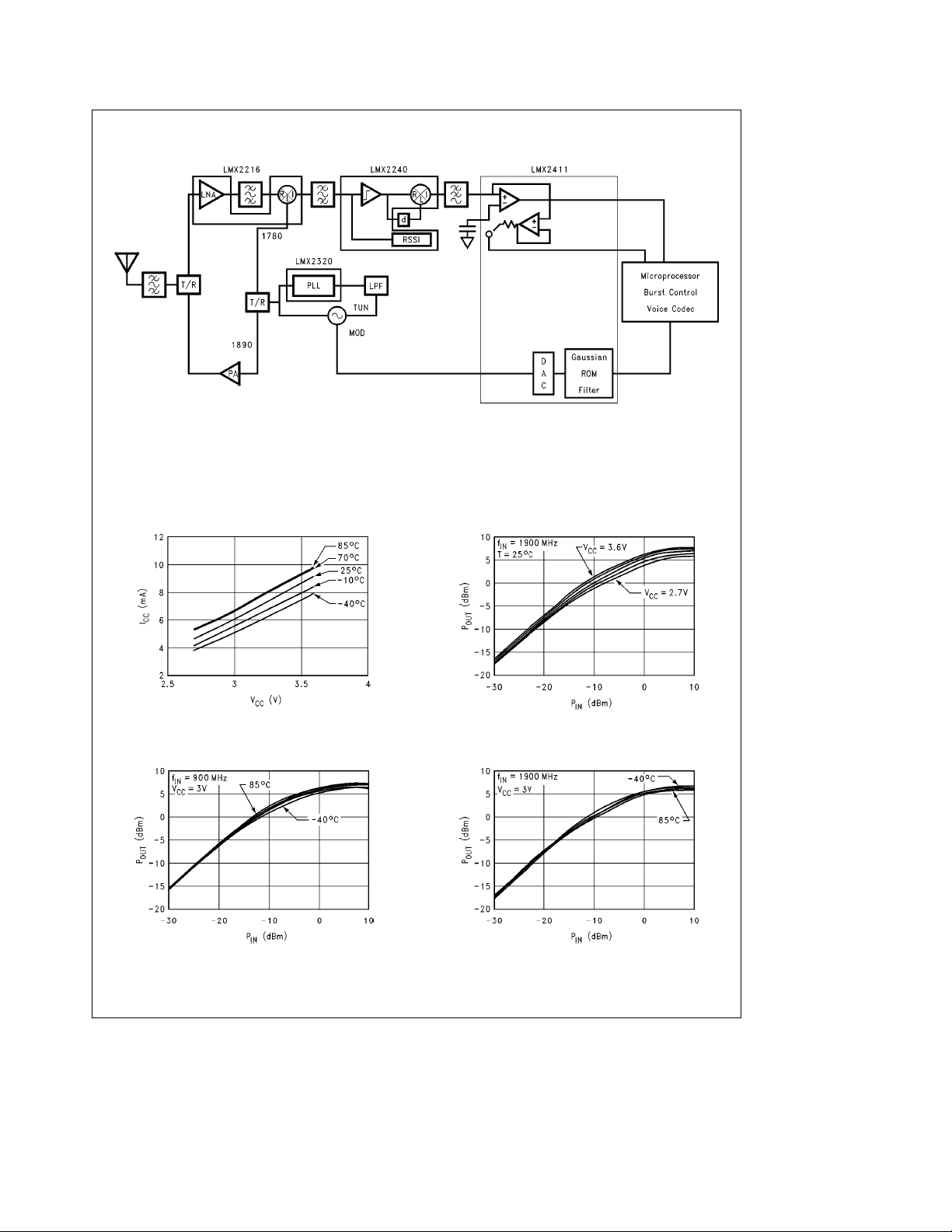
Typical Application Block Diagram
Typical Characteristics
LNA
LNA Current Composition
vs Supply Voltage with
Temperature as a Parameter
LNA P
Temperature as a Parameter
OUT
vs PINwith
TL/W/11814– 3
FIGURE 2
LNA P
Voltage as a Parameter
LNA P
Temperature as a Parameter
vs PINwith Supply
OUT
vs PINwith
OUT
TL/W/11814– 2
TL/W/11814– 4
TL/W/11814– 6
TL/W/11814– 7
4
 Loading...