

LMX1600/LMX1601/LMX1602
PLLatinum
™
Low Cost Dual Frequency Synthesizer
LMX1600 2.0 GHz/500 MHz
LMX1601 1.1 GHz/500 MHz
LMX1602 1.1 GHz/1.1 GHz
General Description
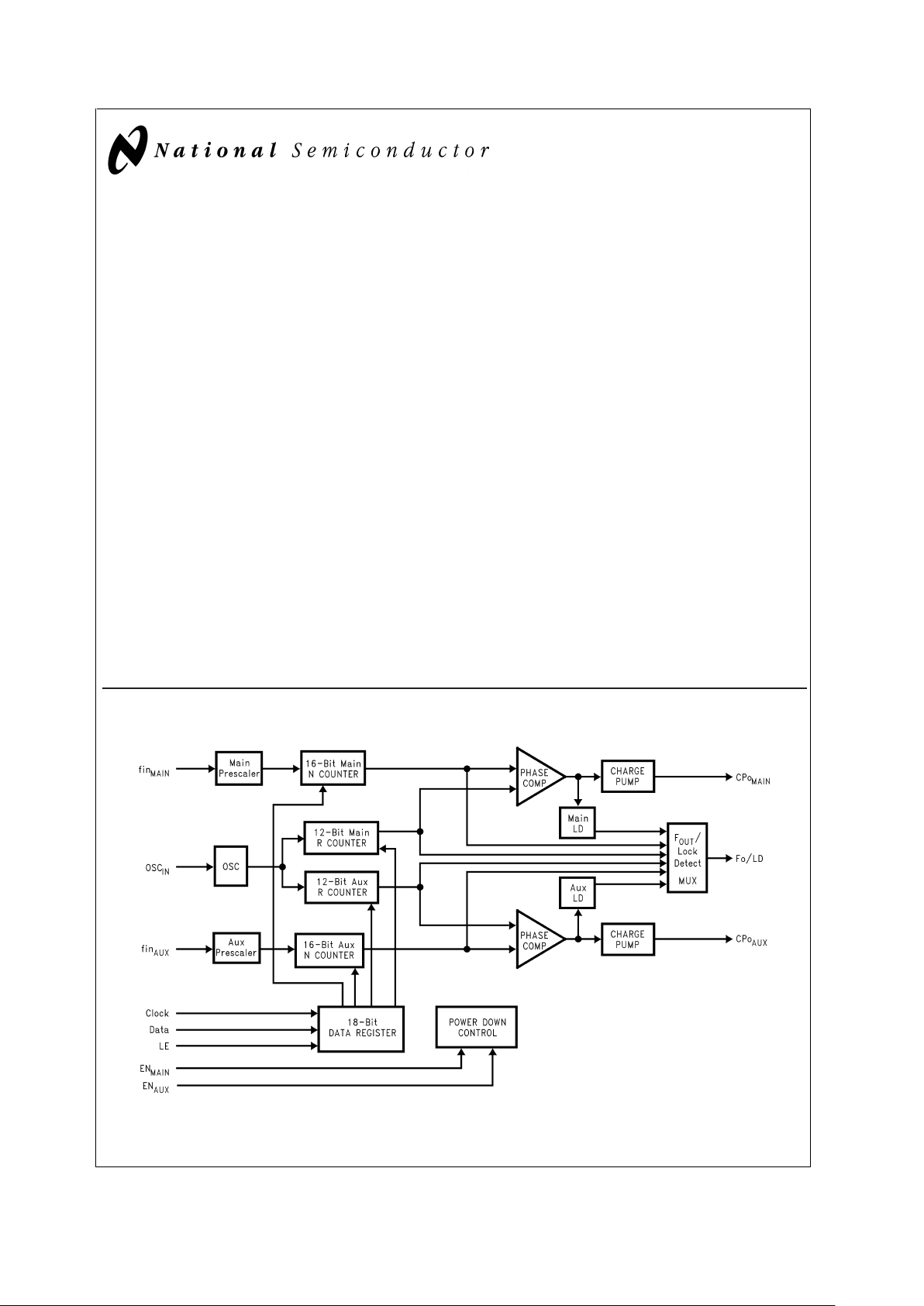
The LMX1600/01/02 is part of a family of monolithic
integrated dual frequency synthesizers designed to be used
in a local oscillator subsystem for a radio transceiver. It is
fabricated using National’s 0.5u ABiC V silicon BiCMOS
process.
The LMX1600/01/02 contains two dual modulus prescalers,
four programmable counters, two phase detectors and two
selectable gain charge pumps necessary to provide the
control voltage for two external loop filters and VCO loops.
Digital filtered lock detects for both PLLs are included. Data
is transferred into the LMX1600/01/02 via a MICROWIRE
™
serial interface (Data, Clock, LE).
V
CC
supply voltage can range from 2.7V to 3.6V. The
LMX1600/01/02 features very low current consumption typically 4.0 mA at 3V for LMX1601, 5.0 mA at 3V for
LMX1600 or LMX1602. Powerdown for the PLL is hardware
controlled.
The LMX1600/01/02 is available in a 16 pin TSSOP surface
mount plastic package.
Features
n VCC= 2.7V to 3.6V operation
n Low current consumption:
4mA
@
3V (typ) for LMX1601
5mA
@
3V (typ) for LMX1600 or LMX1602
n PLL Powerdown mode: I
CC
= 1 µA typical
n Digital Filtered Lock Detects
n Dual modulus prescaler:
— 2 GHz/500 MHz option: (Main) 32/33 (Aux) 8/9
— 1.1 GHz/500 MHz option: (Main) 16/17 (Aux) 8/9
— 1.1 GHz/1.1 GHz option: (Main) 16/17 (Aux) 16/17
Applications
n Cordless / Cellular / PCS phones
n Other digital mobile phones
Functional Block Diagram
TRI-STATE®is a registered trademark of National Semiconductor Corporation.
MICROWIRE
™
and PLLatinum™are trademarks of National Semiconductor Corporation.
DS100129-1
PRELIMINARY
August 2000
LMX1600/LMX1601/LMX1602 PLLatinum Low Cost Dual Frequency Synthesizer
© 2001 National Semiconductor Corporation DS100129 www.national.com

Connection Diagram
Pin Descriptions
Pin No. for
16-pin CSP
Package
Pin No. for
16-pin
TSSOP
Package
Pin Name I/O Description
16 1 FoLD O Multiplexed output of the Main/Aux programmable or reference dividers
and Main/Aux lock detect. CMOS output. (See Programming
Description 2.5)
1 2 OSC
IN
I PLL reference input which drives both the Main and Aux R counter
inputs. Has about 1.2V input threshold and can be driven from an
external CMOS or TTL logic gate. Typically connected to a TCXO
output. Can be used with an external resonator (See Programming
Description 2.5.4).
2 3 OSC
OUT
O Oscillator output. Used with an external resonator.
3 4 GND — Aux PLL ground.
4 5 fin
AUX
I Aux prescaler input. Small signal input from the VCO.
56V
CC
AUX
— Aux PLL power supply voltage input. Must be equal to V
CC
MAIN
. May
range from 2.7V to 3.6V. Bypass capacitors should be placed as close
as possible to this pin and be connected directly to the ground plane.
6 7 CPo
AUX
O Aux PLL Charge Pump output. Connected to a loop filter for driving the
control input of an external VCO.
DS100129-22
Order Number LMX1600SLB, LMX1601SLB, or
LMX1602SLB
NS Package Number SLB16A
DS100129-2
Order Number LMX1600TM, LMX1601TM, or
LMX1602TM
NS Package Number MTC16
LMX1600/LMX1601/LMX1602
www.national.com 2

Connection Diagram (Continued)
Pin Descriptions (Continued)
Pin No. for
16-pin CSP
Package
Pin No. for
16-pin
TSSOP
Package
Pin Name I/O Description
78EN
AUX
I Powers down the Aux PLL when LOW (N and R counters, prescaler,
and tristates charge pump output). Bringing EN
AUX
HIGH powers up the
Aux PLL.
89EN
MAIN
I Powers down the Main PLL when LOW (N and R counters, prescaler,
and tristates charge pump output). Bringing EN
MAIN
HIGH powers up
the Main PLL.
9 10 CPo
MAIN
O Main PLL Charge Pump output. Connected to a loop filter for driving the
control input of an external VCO.
10 11 V
CC
MAIN
— Main PLL power supply voltage input. Must be equal to V
CC
AUX
. May
range from 2.7V to 3.6V. Bypass capacitors should be placed as close
as possible to this pin and be connected directly to the ground plane.
11 12 fin
MAIN
I Main prescaler input. Small signal input from the VCO.
12 13 GND — Main PLL ground.
13 14 LE I Load enable high impedance CMOS input. Data stored in the shift
registers is loaded into one of the 4 internal latches when LE goes
HIGH (control bit dependent).
14 15 Data I High impedance CMOS input. Binary serial data input. Data entered
MSB first. The last two bits are the control bits.
15 16 Clock I High impedance CMOS Clock input. Data for the various counters is
clocked in on the rising edge, into the 18-bit shift register.
LMX1600/LMX1601/LMX1602
www.national.com3
Absolute Maximum Ratings (Notes 2, 1)
If Military/Aerospace specified devices are required, please contact the National Semiconductor Sales
Office/Distributors for availability and specifications.
Value
Parameter Symbol Min Typical Max Unit
V
CC
MAIN
−0.3 6.5 V
Power Supply Voltage V
CC
AUX
−0.3 6.5 V
Voltage on any pin with GND=0V V
I
−0.3 VCC+ 0.3 V
Storage Temperature Range T
S
−65 +150 ˚C
Lead Temp. (solder 4 sec) T
L
+260 ˚C
ESD-Human Body Model (Note 2) 2000 eV
Recommended Operating Conditions
Value
Parameter Symbol Min Typical Max Unit
V
CC
MAIN
2.7 3.6 V
Power Supply Voltage V
CC
AUX
V
CC
MAIN
V
CC
MAIN
V
Operating Temperature T
A
−40 +85 ˚C
Note 1: “Absolute Maximum Ratings” indicate limits beyond which damage to the device may occur. Recommended Operating Conditions indicate conditions for
which the device is intended to be functional, but do not guarantee specific performance limits. Electrical Characteristics document specific minimum and/or
maximum performance values at specified test conditions and are guaranteed. Typical values are for informational purposes only - based on design parameters or
device characterization and are not guaranteed.
Note 2: This device is a high performance RF integrated circuit and is ESD sensitive. Handling and assembly of this device should only be done on ESD-free
workstations.
Electrical Characteristics
(V
CC
MAIN
=V
CC
AUX
= 3.0V; TA= 25˚C except as specified)
Symbol Parameter Conditions Min Typ Max Units
GENERAL
I
CC
Power
Supply
Current
2 GHz + 500 MHz Crystal Mode (Note 3) 5.0 mA
1.1 GHz + 500 MHz Crystal Mode (Note 3) 4.0 mA
1.1 GHz + 1.1 GHz Crystal Mode (Note 3) 5.0 mA
2 GHz Only Crystal Mode (Note 3) 3.5 mA
1.1 GHz Only Crystal Mode (Note 3) 2.5 mA
500 MHz Only Crystal Mode (Note 3) 1.5 mA
I
CC-PWDN
Power Down Current EN
MAIN
= LOW, EN
AUX
= LOW 1 µA
fin fin Operating Frequency fin Main 2 GHz Option 200 2000 MHz
fin Main and Aux 1.1 GHz Option 100 1100 MHz
fin Aux 500 MHz Option 40 500 MHz
OSC
IN
Oscillator Operating Frequency Logic Mode (Note 3) 1 40 MHz
Crystal Mode (Note 3) 1 20 MHz
V
OSC
Oscillator Input Sensitivity 0.5 V
CC
V
PP
fφ Maximum Phase Detector Frequency 10 MHz
Pfin Main and Aux RF Input Sensitivity −15 0 dBm
CHARGE PUMP
ICP
o-source
RF Charge Pump Output Current
(See Programming Description 2.4)
VCPo = VCC/2, High Gain Mode −1600 µA
ICP
o-sink
VCPo = VCC/2, High Gain Mode 1600 µA
ICP
o-source
VCPo = VCC/2, Low Gain Mode −160 µA
ICP
o-sink
VCPo = VCC/2, Low Gain Mode 160 µA
ICP
o-Tri
Charge Pump TRI-STATE®Current 0.5 ≤ VCPo≤ VCC−0.5 1 nA
DIGITAL INTERFACE (DATA, CLK, LE, EN, FoLD)
V
IH
High-Level Input Voltage 0.8V
CC
V
V
IL
Low-Level Input Voltage 0.2V
CC
V
I
IH
High-Level Input Current VIH=VCC= 3.6V, (Note 4) −1.0 1.0 µA
LMX1600/LMX1601/LMX1602
www.national.com 4

Electrical Characteristics (Continued)
(V
CC
MAIN
=V
CC
AUX
= 3.0V; TA= 25˚C except as specified)
Symbol Parameter Conditions Min Typ Max Units
DIGITAL INTERFACE (DATA, CLK, LE, EN, FoLD)
I
IL
Low-Level Input Current VIL= 0V; VCC= 3.6V, (Note 4) −1.0 1.0 µA
I
IH
OSCINInput Current VIH=VCC= 3.6V 100 µA
I
IL
OSCINInput Current VIL= 0V; VCC= 3.6V −100 µA
I
O
OSC
OUT
Output Current Magnitude
(sink/source) (Note 5)
Logic Mode
V
CC
= 3.6V
(Note 3)
|200| µA
V
OUT=VCC
/2 Crystal Mode
V
CC
= 2.7V
(Note 3)
|300| µA
V
OH
High-Level Output Voltage IOH= −500 µA VCC−0.4 V
V
OL
Low-Level Output Voltage IOL= 500 µA 0.4 V
MICROWIRE TIMING
t
CS
Data to Clock Set Up Time See Data Input Timing 50 ns
t
CH
Data to Clock Hold Time See Data Input Timing 10 ns
t
CWH
Clock Pulse Width High See Data Input Timing 50 ns
t
CWL
Clock Pulse Width Low See Data Input Timing 50 ns
t
ES
Clock to Load Enable Set Up Time See Data Input Timing 50 ns
t
EW
Load Enable Pulse Width See Data Input Timing 50 ns
CLOSED LOOP SYNTHESIZER PERFORMANCE (NSC evaluation board only)
RFφ
n
Main PLL Phase Noise Floor (Note 6) −160 dBc/Hz
Note 3: Refer to Programming Description 2.5.3.
Note 4: Except fin.
Note 5: The OSCout Output Current Magnitude is lass than or equal to 200µA when the Logic Mode is selected. The OSCout Output Current Magnitude is greater
than or equal to 300µA when the Crystal Mode is selected.
Note 6: Offset frequency = 1 kHz, fin = 900 MHz, fφ = 25 kHz, N = 3600, f
OSC
= 10 MHz, V
OSC
>
1.2 VPP. Refer to the Application Note, AN-1052, for description
of phase noise floor measurement.
LMX1600/LMX1601/LMX1602
www.national.com5
 Loading...