


December 1999
LMV921 Single/ LMV922 Dual/ LMV924 Quad
1.8V, 1MHz, Low Power Operational Amplifiers with
Rail-To-Rail Input and Output
LMV921 Single/ LMV922 Dual/ LMV924 Quad 1.8V, 1MHz, Low Power Operational Amplifiers with
Rail-To-Rail Input and Output
General Description
The LMV921 Single/LMV922 Dual/LMV924 Quad are guaranteed to operate from +1.8V to +5.0V supply voltages and
have rail-to-rail input and output. This rail-to-rail operation
enables the user to make full use of the entire supply voltage
range. The input common mode voltage range extends
300mV beyond the supplies and the output can swing
rail-to-rail unloaded and within 100mV from the rail with
600Ω load at 1.8V supply. The LMV921/LMV922/LMV924
are optimized to work at 1.8V which make them ideal for portable two-cell battery-powered systems and single cell Li-Ion
systems.
The LMV921/LMV922/LMV924 exhibit excellent
speed-power ratio, achieving 1MHz gain bandwidth product
at 1.8V supply voltage with very low supply current. The
LMV921/LMV922/LMV924 are capable of driving 600Ω load
and up to 1000pF capacitive load with minimal ringing. The
LMV921/LMV922/LMV924’s high DC gain of 100dB makes
them suitable for low frequency applications.
The LMV921 (Single) is offered in a space saving SC70–5
and SOT23–5 packages. The SC70–5 package is only
2.0X2.1X1.0mm. These small packages are ideal solutions
for area constrained PC boards and portable electronics
such as cellphones and PDAs.
Connection Diagrams
5-Pin SC70-5/SOT23-5
Features
(Typical 1.8V Supply Values; Unless Otherwise Noted)
n Guaranteed 1.8V, 2.7V and 5V specifications
n Rail-to-Rail input & output swing
— w/600Ω load 100 mV from rail
— w/2kΩ load 30 mV from rail
n V
CM
n 90dB gain w/600Ω load
n Supply current 145µA/amplifier
n Gain bandwidth product 1MHz
n LMV921 Maximum V
n LMV921 available in Ultra Tiny, SC70-5 package
n LMV922 available in MSOP-8 package
n LMV924 available in TSSOP-14 package
OS
300mV beyond rails
6mV
Applications
n Cordless/cellular phones
n Laptops
n PDAs
n PCMCIA
n Portable/battery-powered electronic Equipment
n Supply current Monitoring
n Battery monitoring
8-Pin MSOP/SOIC
DS100979-84
Top View
DS100979-2
Top View
© 1999 National Semiconductor Corporation DS100979 www.national.com

Connection Diagrams (Continued)
14-Pin TSSOP/SOIC
DS100979-1
Top View
Ordering Information
LMV921 Single/ LMV922 Dual/ LMV924 Quad
Package Temperature Range
Industrial
−40˚C to +85˚C
5-Pin SC70-5 LMV921M7 A21 1k Units Tape and Reel MAA05A
LMV921M7X A21 3k Units Tape and Reel
5-Pin SOT23-5 LMV921M5 A29A 1k Units Tape and Reel
LMV921M5X A29A 3k Units Tape and Reel
8-Pin MSOP LMV922MM LMV922 1k Units Tape and Reel
LMV922MMX LMV922 3.5k Units Tape and Reel
14-Pin TSSOP LMV924MT LMV924 Rails
LMV924MTX LMV924 2.5k Units Tape and Reel
8-Pin SOIC LMV922M LMV922M Rails
LMV922MX LMV922M 2.5k Units Tape and Reel
14-Pin SOIC LMV924M LMV924M Rails
LMV924MX LMV924M 2.5k Units Tape and Reel
Packaging
Marking
Transport Media NSC
Drawing
MA05B
MUA08A
MTC14
M08A
M14A
www.national.com 2

Absolute Maximum Ratings (Note 1)
If Military/Aerospace specified devices are required,
please contact the National Semiconductor Sales Office/
Distributors for availability and specifications.
ESD Tolerance (Note 2)
Machine Model 100V
Human Body Model 2000V
Differential Input Voltage
Supply Voltage (V
Output Short Circuit to V
Output Short Circuit to V
+–V−
) 5.5V
+
(Note 3)
−
(Note 3)
Storage Temperature Range −65˚C to 150˚C
Junction Temperature (Note 4) 150˚C
Mounting Temp.
Infrared or Convection (20 sec) 235˚C
±
Supply Voltage
Operating Ratings (Note 1)
Supply Voltage 1.5V to 5.0V
Temperature Range −40˚C ≤ T
Thermal Resistance (θ
Ultra Tiny SC70-5 Package
5-Pin Surface Mount 440 ˚C/W
Tiny SOT23-5 Package
5-Pin Surface Mount 265 ˚C/W
MSOP Package
8-Pin Surface Mount 235˚C/W
TSSOP Package
14-Pin Surface Mount 155˚C/W
SOIC Package
8-Pin Surface Mount 175˚C/W
14-Pin Surface Mount 127˚C/W
)
JA
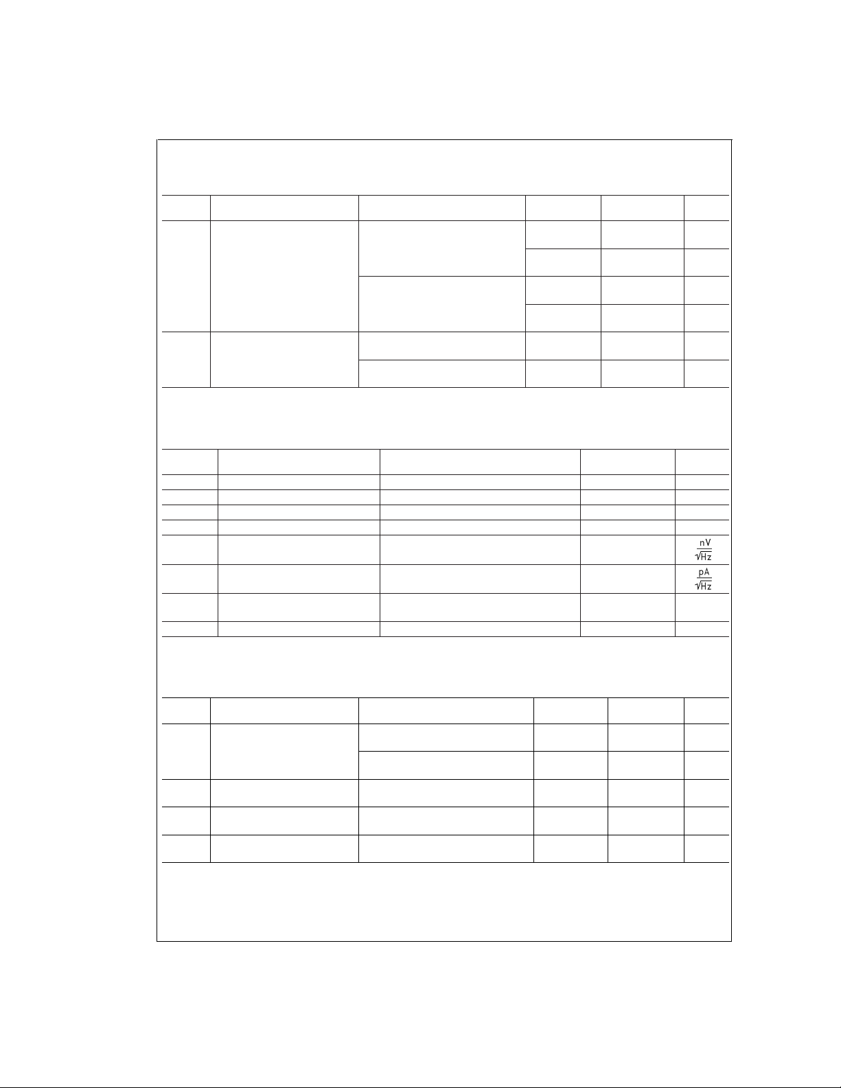
1.8V DC Electrical Characteristics
Unless otherwise specified, all limits guaranteed for TJ= 25˚C. V+= 1.8V, V−= 0V, VCM=V+/2, VO=V+/2 and
>
1MΩ.Boldface limits apply at the temperature extremes.
R
L
Symbol Parameter Condition Typ
V
OS
Input Offset Voltage LMV921 (Single) −1.8 6
LMV922 (Dual)
(Note 5)
−1.8 8
LMV924 (Quad)
TCV
I
B
I
OS
I
S
Input Offset Voltage Average
OS
Drift
Input Bias Current 12 35
Input Offset Current 2 25
Supply Current LMV921 (Single) 145 185
1 µV/˚C
LMV922 (Dual) 330 400
LMV924 (Quad) 560 700
CMRR Common Mode Rejection Ratio 0 ≤ V
PSRR Power Supply Rejection Ratio 1.8V ≤ V
V
CM
Input Common-Mode Voltage
Range
≤ 0.6V 82 62
CM
−0.2V ≤ V
1.8V ≤ V
= 0.5V
V
CM
CM
+
CM
≤ 2.0V
≤ 5V,
≤ 0V
74 50
78 67
For CMRR ≥ 50dB -0.3 -0.2
2.15 2.0
A
V
Large Signal Voltage Gain
LMV921 (Single)
Large Signal Voltage Gain
LMV922 (Dual)
LMV924 (Quad)
RL= 600Ω to 0.9V,
= 0.2V to 1.6V, VCM= 0.5V
V
O
=2kΩto 0.9V,
R
L
= 0.2V to 1.6V, VCM= 0.5V
V
O
= 600Ω to 0.9V,
R
L
= 0.2V to 1.6V, VCM= 0.5V
V
O
=2kΩto 0.9V,
R
L
= 0.2V to 1.6V, VCM= 0.5V
V
O
91 77
95 80
79 65
83 68
Limits
(Note 6)
9.5
50
40
205
550
850
60
62
1.8
73
75
61
63
LMV921 Single/ LMV922 Dual/ LMV924 Quad
≤ 85˚C
J
Units
8
0
mV
max
mV
max
nA
max
nA
max
µA
max
dB
min
dB
min
V
max
V
min
dB
min
dB
min
www.national.com3
1.8V DC Electrical Characteristics (Continued)
Unless otherwise specified, all limits guaranteed for TJ= 25˚C. V+= 1.8V, V−= 0V, VCM=V+/2, VO=V+/2 and
>
R
1MΩ.Boldface limits apply at the temperature extremes.
L
Symbol Parameter Condition Typ
V
O
Output Swing RL= 600Ω to 0.9V
=±100mV
V
IN
(Note 5)
1.7 1.65
Limits
(Note 6)
1.63
0.075 0.090
0.105
R
=2kΩto 0.9V
L
=±100mV
V
IN
1.77 1.75
1.74
0.025 0.035
0.040
I
O
LMV921 Single/ LMV922 Dual/ LMV924 Quad
Output Short Circuit Current Sourcing, VO=0V
= 100mV
V
IN
Sinking, V
V
IN
O
= −100mV
= 1.8V
64
3.3
10 7
5
1.8V AC Electrical Characteristics
Unless otherwise specified, all limits guaranteed for TJ= 25˚C. V+= 1.8V, V−= 0V, VCM=V+/2, VO=V+/2 and
>
R
1MΩ.Boldface limits apply at the temperature extremes.
L
Symbol Parameter Conditions Typ
SR Slew Rate (Note 7) 0.39 V/µs
GBW Gain-Bandwidth Product 1 MHz
Φ
m
G
m
e
n
Phase Margin 60 Deg.
Gain Margin 10 dB
Input-Referred Voltage Noise f = 1 kHz, VCM= 0.5V 45
(Note 5)
Units
V
min
V
max
V
min
V
max
mA
min
mA
min
Units
i
n
THD Total Harmonic Distortion f=1kHz, A
Input-Referred Current Noise f = 1 kHz 0.1
=
+1
V
R
L
=
600kΩ,V
=
1V
IN
PP
Amp-to-Amp Isolation (Note 8) 140 dB
2.7V DC Electrical Characteristics
Unless otherwise specified, all limits guaranteed for TJ= 25˚C. V+= 2.7V, V−= 0V, VCM=V+/2, VO=V+/2 and
>
R
1MΩ.Boldface limits apply at the temperature extremes.
L
Symbol Parameter Condition Typ
V
OS
Input Offset Voltage LMV921 (Single) −1.6 6
LMV922 (Dual)
LMV924 (Quad)
TCV
I
B
I
OS
www.national.com 4
Input Offset Voltage Average
OS
Drift
Input Bias Current 12 35
Input Offset Current 2 25
(Note 5)
−1.6 8
1 µV/˚C
0.089
(Note 6)
Limits
8
9.5
50
40
%
Units
mV
max
mV
max
nA
max
nA
max

2.7V DC Electrical Characteristics (Continued)
Unless otherwise specified, all limits guaranteed for TJ= 25˚C. V+= 2.7V, V−= 0V, VCM=V+/2, VO=V+/2 and
>
R
1MΩ.Boldface limits apply at the temperature extremes.
L
Symbol Parameter Condition Typ
I
S
Supply Current LMV921 (Single) 147 190
LMV922 (Dual) 380 450
LMV924 (Quad) 580 750
CMRR Common Mode Rejection Ratio 0V ≤ V
−0.2V ≤ V
2.7V ≤ V
PSRR Power Supply Rejection Ratio 1.8V ≤ V
V
V
CM
A
V
Input Common-Mode Voltage
Range
Large Signal Voltage Gain
LMV921 (Single)
For CMRR ≥ 50dB -0.3 -0.2
RL= 600Ω to 1.35V,
V
R
V
Large Signal Voltage Gain
LMV922 (Dual)
LMV924 (Quad)
R
V
R
V
V
O
Output Swing RL= 600Ω to 1.35V
V
R
V
I
O
Output Short Circuit Current Sourcing, VO=0V
V
Sinking, V
V
≤ 1.5V 84 62
CM
≤ 0V
CM
<
2.9V
CM
+
≤ 5V,
= 0.5V
CM
= 0.2V to 2.5V
O
=2kΩto 1.35V,
L
= 0.2V to 2.5V
O
= 600Ω to 1.35V,
L
= 0.2V to 2.5V
O
=2kΩto 1.35V,
L
= 0.2V to 2.5V
O
=±100mV
IN
=2kΩto 1.35V
L
=±100mV
IN
= 100mV
IN
IN
O
= −100mV
= 2.7V
(Note 5)
(Note 6)
73 50
78 67
3.050 2.9
98 80
103 83
86 68
91 71
2.62 2.550
0.075 0.095
2.675 2.650
0.025 0.040
27 20
28 22
Limits
210
600
900
60
62
0
2.7
75
77
63
65
2.530
0.115
2.640
0.045
15
16
LMV921 Single/ LMV922 Dual/ LMV924 Quad
Units
uA
max
dB
min
dB
min
V
max
V
min
dB
min
dB
min
V
min
V
max
V
min
V
max
mA
min
mA
min
2.7V AC Electrical Characteristics
Unless otherwise specified, all limits guaranteed for TJ= 25˚C. V+= 2.7V, V−= 0V, VCM= 1.0V, VO= 1.35V and
>
1MΩ.Boldface limits apply at the temperature extremes.
R
L
Symbol Parameter Conditions Typ
(Note 5)
SR Slew Rate (Note 7) 0.41 V/µs
GBW Gain-Bandwidth Product 1 MHz
Φ
m
G
m
e
n
i
n
Phase Margin 65 Deg.
Gain Margin 10 dB
Input-Referred Voltage Noise f = 1 kHz, VCM= 0.5V 45
Input-Referred Current Noise f = 1 kHz 0.1
Units
www.national.com5

2.7V AC Electrical Characteristics (Continued)
Unless otherwise specified, all limits guaranteed for TJ= 25˚C. V+= 2.7V, V−= 0V, VCM= 1.0V, VO= 1.35V and
>
R
1MΩ.Boldface limits apply at the temperature extremes.
L
Symbol Parameter Conditions Typ
=
THD Total Harmonic Distortion f=1 kHz, A
=
600kΩ,V
R
L
+1
V
=
1V
IN
PP
Amp-to-Amp Isolation (Note 8) 140 dB
5V DC Electrical Characteristics
Unless otherwise specified, all limits guaranteed for TJ= 25˚C. V+= 5V, V−= 0V, VCM=V+/2, VO=V+/2 and
>
R
1MΩ.Boldface limits apply at the temperature extremes.
L
Symbol Parameter Condition Typ
V
LMV921 Single/ LMV922 Dual/ LMV924 Quad
OS
Input Offset Voltage LMV921 (Single) −1.5 6
LMV922 (Dual)
LMV924 (Quad)
TCV
I
B
I
OS
I
S
Input Offset Voltage Average
OS
Drift
Input Bias Current 12 35
Input Offset Current 2 25
Supply Current LMV921 (Single) 160 210
LMV922 (Dual) 400 500
LMV924 (Quad) 750 850
CMRR Common Mode Rejection Ratio 0V ≤ V
−0.2V ≤ V
5.0V ≤ V
PSRR Power Supply Rejection Ratio 1.8V ≤ V
V
V
CM
A
V
Input Common-Mode Voltage
Range
Voltage Gain
LMV921 (Single)
For CMRR ≥ 50dB -0.3 -0.2
RL= 600Ω to 2.5V
V
R
V
Voltage Gain
LMV922 (Dual)
LMV924 (Quad)
R
V
R
V
≤ 3.8V 86 62
CM
≤ 0V
CM
≤ 5.2V
CM
+
≤ 5V
= 0.5V
CM
= 0.2V to 4.8V
O
=2kΩto 2.5V
L
= 0.2V to 4.8V
O
= 600Ω to 2.5V
L
= 0.2V to 4.8V
O
=2kΩto 2.5V
L
= 0.2V to 4.8V
O
(Note 5)
−1.5 8
1 µV/˚C
72 50
78 67
5.350 5.2
104 86
108 89
90 72
96 77
(Note 5)
0.077
Limits
(Note 6)
8
9.5
50
40
230
700
980
61
62
0
5.0
82
85
68
73
Units
%
Units
mV
max
mV
max
nA
max
nA
max
µA
max
dB
min
dB
min
V
max
V
min
dB
min
dB
min
www.national.com 6

5V DC Electrical Characteristics (Continued)
Unless otherwise specified, all limits guaranteed for TJ= 25˚C. V+= 5V, V−= 0V, VCM=V+/2, VO=V+/2 and
>
R
1MΩ.Boldface limits apply at the temperature extremes.
L
Symbol Parameter Condition Typ
V
O
Output Swing RL= 600Ω to 2.5V
=±100mV
V
IN
(Note 5)
4.895 4.865
Limits
(Note 6)
4.840
0.1 0.135
0.160
R
=2kΩto 2.5V
L
=±100mV
V
IN
4.965 4.945
4.935
0.035 0.065
0.075
I
O
Output Short Circuit Current LMV921 Sourcing, VO=0V
= 100mV
V
IN
LMV922, LMV924 Sourcing, V
0V
= 100mV
V
IN
Sinking, V
V
IN
O
= −100mV
=5V
=
O
98 85
68
60 35
75 65
45
5V AC Electrical Characteristics
Unless otherwise specified, all limits guaranteed for TJ= 25˚C. V+= 5V, V−= 0V, VCM=V+/2, VO= 2.5V and
>
R
1MΩ.Boldface limits apply at the temperature extremes.
L
Symbol Parameter Conditions Typ
SR Slew Rate (Note 7) 0.45 V/µs
GBW Gain-Bandwidth Product 1 MHz
Φ
m
G
m
e
n
Phase Margin 70 Deg.
Gain Margin 15 dB
Input-Referred Voltage Noise f = 1 kHz, VCM=1V 45
(Note 5)
LMV921 Single/ LMV922 Dual/ LMV924 Quad
Units
V
min
V
max
V
min
V
max
mA
min
mA
min
Units
i
n
THD Total Harmonic Distortion f = 1 kHz, AV=+1
Input-Referred Current Noise f = 1 kHz 0.1
0.069
= 600Ω,VO=1V
R
L
PP
%
Amp-to-Amp Isolation (Note 8) 140 dB
Note 1: Absolute Maximum Ratings indicate limits beyond which damage to the device may occur. Operating Ratings indicate conditions for which the device is intended to be functional, but specific performance is not guaranteed. For guaranteed specifications and the test conditions, see the Electrical Characteristics.
Note 2: Human body model, 1.5 kΩ in series with 100 pF. Machine model, 200Ω in series with 100 pF.
Note 3: Applies to both single-supply and split-supply operation. Continuous short circuit operation at elevated ambient temperature can result in exceeding the
maximum allowed junction temperature of 150˚C. Output currents in excess of 45 mA over long term may adversely affect reliability.
Note 4: The maximum power dissipation is a function of T
=(T
P
D
Note 5: Typical Values represent the most likely parametric norm.
Note 6: All limits are guaranteed by testing or statistical analysis.
Note 7: V
Note 8: Input referred, V
)/θJA. All numbers apply for packages soldered directly into a PC board.
J(max)–TA
+
= 5V. Connected as voltage follower with 5V step input. Number specified is the slower of the positive and negative slew rates.
+
=
5V and R
=
100kΩ connected to 2.5V. Each amp excited in turn with 1kHz to produce V
L
, θJA, and TA. The maximum allowable power dissipation at any ambient temperature is
J(max)
=
.
3V
O
PP
www.national.com7

Simplified Schematic
LMV921 Single/ LMV922 Dual/ LMV924 Quad
DS100979-A9
www.national.com 8

Typical Performance Characteristics Unless otherwise specified, V
Supply Current vs.
Supply Voltage (LMV921)
Input Bias Current
vs. V
CM
Sourcing Current vs.
Output Voltage
= +5V, single supply, TA= 25˚C.
S
LMV921 Single/ LMV922 Dual/ LMV924 Quad
Sourcing Current vs.
Output Voltage
Sinking Current vs.
Output Voltage
DS100979-A1
DS100979-B8
Sourcing Current vs.
Output Voltage
Sinking Current vs.
Output Voltage
DS100979-D5
DS100979-B2
DS100979-B3
Sinking Current vs.
Output Voltage
DS100979-B4
Offset Voltage vs.
Common Mode Voltage
DS100979-B7
DS100979-B1
DS100979-D1
www.national.com9
 Loading...