NSC LMV7255M7, LMV7255M5X, LMV7255M5, LMV7251M7X, LMV7251M5X Datasheet
...
January 2001
LMV7251/LMV7255
1.8V Low Voltage Comparator with Rail-to-Rail Input
LMV7251/LMV7255 1.8V Low Voltage Comparator with Rail-to-Rail Input
General Description
The LMV7251/LMV7255 are rail-to-rail input low voltage
comparators, which can operate at supply voltage range of
1.8V to 5.0V. The LMV7251/LMV7255 are available in space
saving SC-70 or SOT23-5 packages. These comparators
are ideal for low voltage and space critical designs.
The LMV7251featuresapush-pull output stage. This feature
allows operation with minimum power consumption when
driving a load.
The LMV7255 features an open drain output. This allows the
connection of an external resistor at the output. The output of
the comparator can be used as a level shifter.
The IC’s are built with National Semiconductor’s advance
Submicron Silicon-Gate BiCMOS process. The
LMV7251/LMV7255 have bipolar inputs for improved noise
performance and CMOS outputs for better rail-to-rail output
performance.
Features
(VS= 1.8V, TA= 25˚C, Typical values unless specified).
n Single or Dual Supplies
n Low supply voltage 1.8V to 5.0V
n Ultra low supply current 11µA
n Low input bias current 14nA
n Low input offset current 200pA
n Low input offset voltage +/−0.3mV
n Response time 670ns (20mV overdrive)
n Input common mode voltage 0.1V beyond rails
Applications
n Mobile communications
n Laptops and PDA’s
n Battery powered electronics
n General purpose low voltage applications
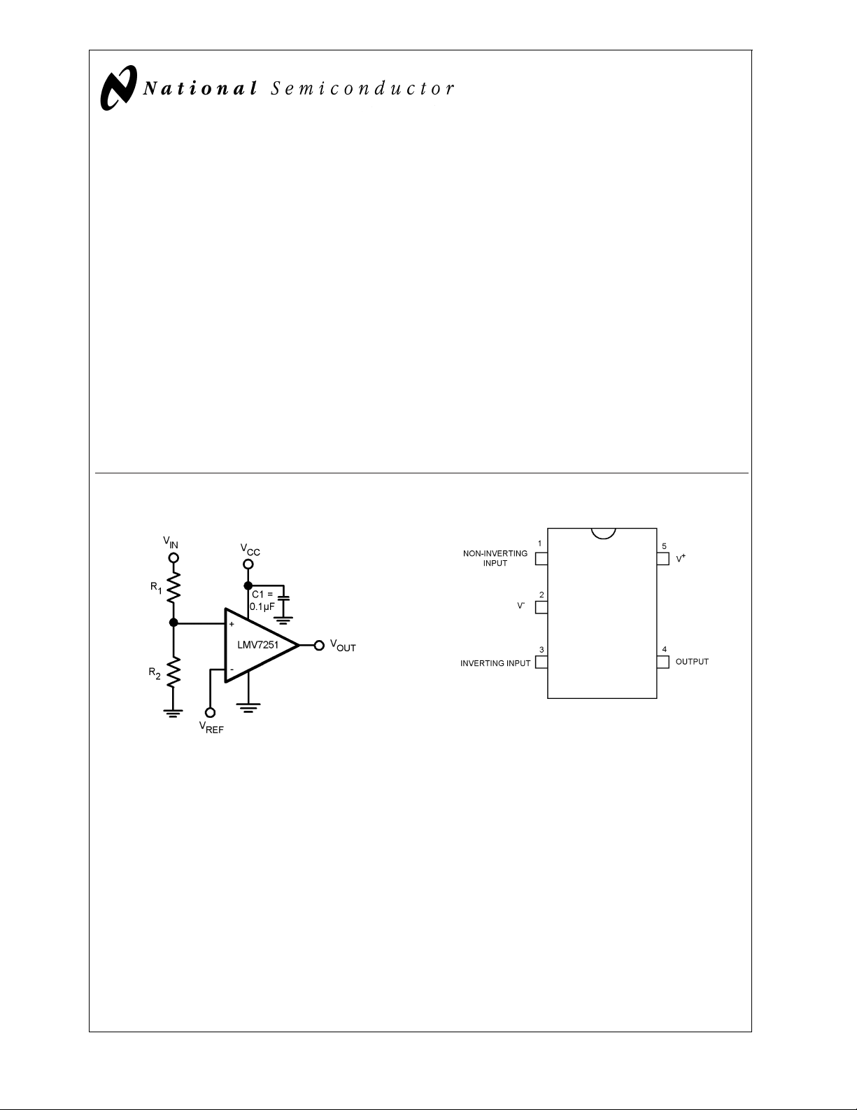
Typical Circuit Connection Diagram
DS200057-1
Top View
DS200057-2
FIGURE 1. Threshold Detector
© 2001 National Semiconductor Corporation DS200057 www.national.com

Absolute Maximum Ratings (Note 1)
If Military/Aerospace specified devices are required,
please contact the National Semiconductor Sales Office/
Wave Soldering (10 sec.) 260˚C
Storage Temperature Range −65˚C to +150˚C
Junction Temperature (Note 4) +150˚C
Distributors for availability and specifications.
ESD Tolerance 1KV (Note 2)
LMV7251/LMV7255
V
Differential +/−Supply Voltage
IN
Supply Voltage (V
Voltage at Input/Output pins V
+-V−
) 5.5V
+
+0.1V, V−−0.1V
Soldering Information
Infrared or Convection (20
200V (Note 6)
Operating Ratings (Note 1)
Supply Voltage V
Junction Temperature Range (Note
3) −40˚C to +85˚C
Package Thermal Resisance (Note 3)
SOT23-5 325˚C/W
SC-70 265˚C/W
+
sec.) 235˚C
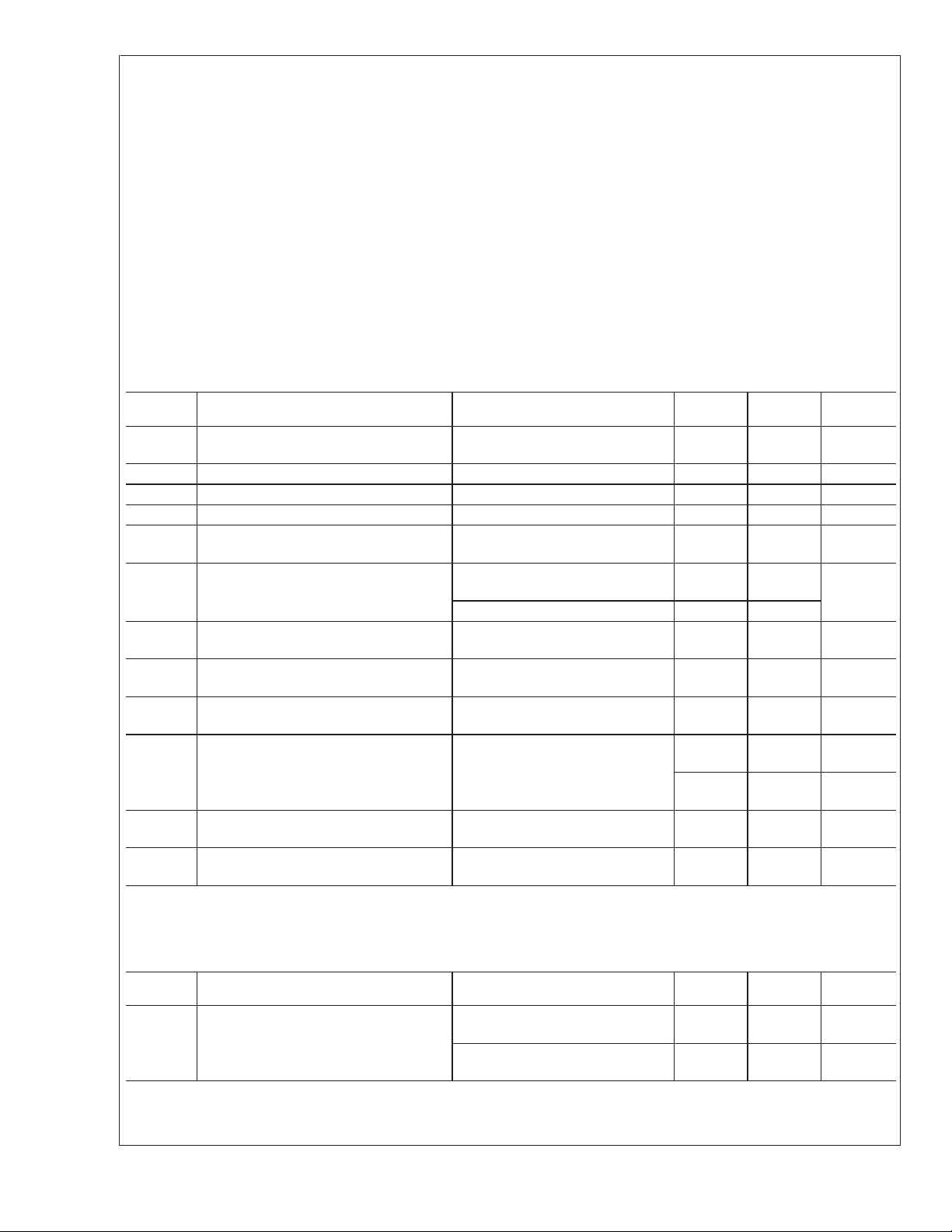
1.8V Electrical Characteristics
Unless otherwise specified, all limits guaranteed for TJ= 25˚C, V+= 1.8V, V−= 0V. Boldface limits apply at the temperature
extremes.
Symbol Parameter Condition Typ
(Note 4)
V
OS
TC V
I
B
I
OS
I
S
I
SC
Input Offset Voltage 0.3 6
Input Offset Average Drift VCM= 0.9V (Note 7) 10 uV/C
OS
Input Bias Current 14 nA
Input Offset Current 200 pA
Supply Current 11 15
Output Short Circuit Current Sourcing, VO= 0.9V
(LMV7251 only)
= 0.9V 11.6 5
O
300 pA
I
LEAKAGE
Sinking, V
Output Leakage Current VO= 1.8V
(LMV7255 only)
V
OH
Output Voltage High IO= 1.5mA
1.72 1.675 V
(LMV7251 only)
V
OL
V
CM
CMRR Common Mode Rejection Ratio 0
PSRR Power Supply Rejection Ratio V
Output Voltage Low IO= −1.5mA 65 125 mV
Input Common Voltage Range CMRR>45 dB 1.9 V
<
<
V
1.8V 72 47 dB
CM
+
= 1.8V to 5V 79 55 dB
84
Limits
(Note 5)
8
17
−0.1 V
1.8V to 5.0V
Units
mV
max
µA
max
mA
min
min
max
max
min
min
min
1.8V AC Electrical Characteristics
Unless otherwise specified, all limits guaranteed for TJ= 25˚C, V+= 1.8V, V−= 0V, VCM= 0.5V, VO=V+/2. Boldface limits
apply at the temperature extremes.
Symbol Parameter Condition Typ
t
PHL
Propagation Delay
(High to Low)
Input Overdrive = 20mV
Load = 50pF//5kΩ
Input Overdrive = 50mV
Load = 50pF//5kΩ
www.national.com 2
(Note 5)
720 ns
380 ns
Limits
(Note 6)
Units

1.8V AC Electrical Characteristics (Continued)
Unless otherwise specified, all limits guaranteed for TJ= 25˚C, V+= 1.8V, V−= 0V, VCM= 0.5V, VO=V+/2. Boldface limits
apply at the temperature extremes.
Symbol Parameter Condition Typ
(Note 5)
t
PLH
Propagation Delay
(Low to High)
Input Overdrive = 20mV
Load = 50pF//5kΩ
Input Overdrive = 50mV
670 ns
400 ns
Limits
(Note 6)
Load = 50pF//5kΩ
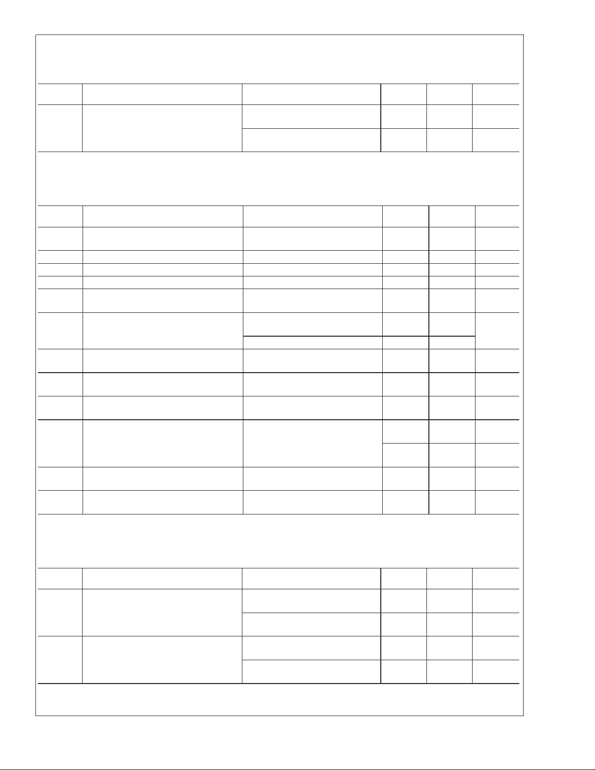
2.7V Electrical Characteristics
Unless otherwise specified, all limits guaranteed for TJ= 25˚C, V+= 2.7V, V−= 0V. Boldface limits apply at the temperature
extremes.
Symbol Parameter Conditions Typ
(Note 5)
V
OS
TC V
I
B
I
OS
I
S
I
SC
Input Offset Voltage 0.03 6
Input Offset Average Drift VCM= 1.35V (Note 7) 10 µV/C
OS
Input Bias Current 15 nA
Input offset Current 210 pA
Supply Current 11 18
Output Short Circuit Current Sourcing, VO= 1.35V
(LMV7251 only)
I
LEAKAGE
Sinking, V
Output Leakage Current VO= 2.7V,
= 1.35V 28 15
O
320 pA
(LMV7255 only)
V
OH
Output Voltage High IO= 2mA
2.63 2.575 V
(LMV7251 only)
V
OL
V
CM
CMRR Common Mode Rejection Ratio 0
PSRR Power Supply Rejection Ratio V
Output Voltage Low IO= −2mA 61 125 mV
Input Common Voltage Range CMRR>45dB 2.8 V
<
<
V
2.7V 75 46 dB
CM
+
= 1.8V to 5V 79 55 dB
28 15
Limits
(Note 6)
8
22
−0.1 V
LMV7251/LMV7255
Units
Units
mV
max
µA
max
mA
min
max
max
min
min
min
2.7V AC Electrical Characteristics
Unless otherwise specified, all limits guaranteed for TJ= 25˚C, V+= 2.7V, V−= 0V.Boldface limits apply at the temperature
extremes.
Symbol Parameter Condition Typ
(Note 5)
t
PHL
Propagation Delay
(High to Low)
Input Overdrive = 20mV
Load = 50pF//5kΩ
Input Overdrive = 50mV
830 ns
430 ns
Load = 50pF//5kΩ
t
PLH
Propagation Delay
(Low to High)
Input Overdrive = 20mV
Load = 50pF//5kΩ
Input Overdrive = 50mV
730 ns
410 ns
Load = 50pF//5kΩ
Limits
(Note 6)
www.national.com3
Units

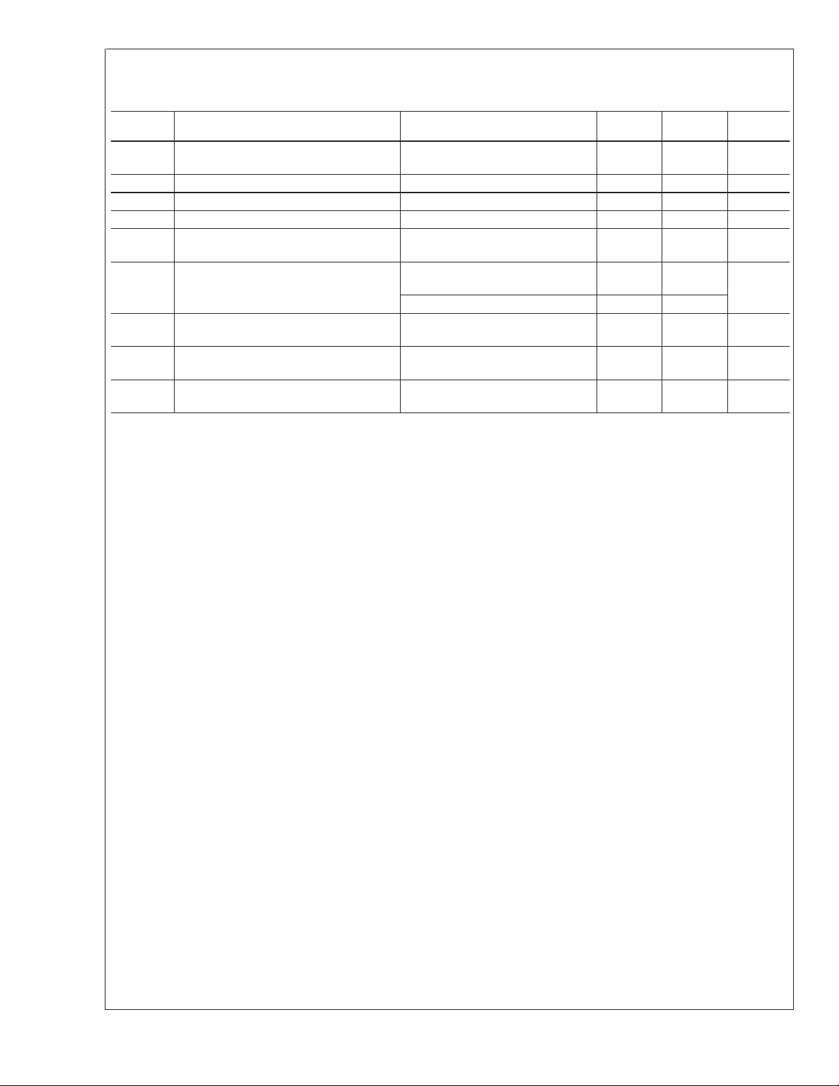
5V Electrical Characteristics
Unless otherwise specified, all limits guaranteed for TJ= 25˚C, V+= 5V, V−= 0V. Boldface limits apply at the temperature extremes.
Symbol Parameter Conditions Typ
(Note 5)
V
OS
Input Offset Voltage 0.03 6
LMV7251/LMV7255
TC V
I
B
I
OS
I
S
I
SC
I
LEAKAGE
V
OH
V
OL
Note 1: Absolute Maximum Ratings indicate limits beyond which damage to the device may occur. Operating Ratings indicate conditions for which the device is
intended to be functional, but specific performance is not guaranteed. For guaranteed specifications and the test conditions, see the Electrical Characteristics.
Note 2: Human body model, 1.5kΩ in series with 100pF.
Note 3: The maximum power dissipation is a function of T
=(T
P
D
Note 4: Typical values represent the most likely parametric norm.
Note 5: All limits are guaranteed by testing or statistical analysis.
Note 6: Machine Model, 0Ω in series with 200pF.
Note 7: Offset Voltage average drift determined by dividing the change in V
Input Offset Average Drift VCM= 2.5V (Note 7) 10 µV/C
OS
Input Bias Current 16 nA
Input Offset Current 220 pA
Supply Current 12 20
Output Short Circuit Current Sourcing, VO= 2.5V
82 50
(LMV7251 only)
Sinking, V
Output Leakage Current VO= 5V,
= 2.5V 78 50
O
375 pA
(LMV7255 only)
Output Voltage High IO= 4mA 4.9 4.82 V
Output Voltage Low IO= −4mA 90 180 mV
, θJA, and TA. The maximum allowable power dissipation at any ambient temperature is
J(max)-TA
)/θJA. All numbers apply for packages soldered directly into a PC board.
J(max)
at temperature extremes into the total temperature change.
OS
Limits
(Note 6)
8
25
Units
mV
max
µA
max
mA
min
min
max
www.national.com 4
 Loading...