

NSC LMH1982SQX, LMH1982 Datasheet
PRELIMINARY
April 9, 2008
LMH1982
Multi-Rate Video Clock Generator with Genlock
General Description
The LMH1982 is a multi-rate video clock generator ideal for
use in a wide range of 3-Gbps (3G), high-definition (HD), and
standard-definition (SD) video applications, such as video
synchronization, serial digital interface (SDI) serializer and
deserializer (SerDes), video conversion, video editing, and
other broadcast and professional video systems.
The LMH1982 can generate two simultaneous SD and HD
clocks and a Top of Frame (TOF) pulse. In genlock mode, the
device's phase locked loops (PLLs) can synchronize the output signals to H sync and V sync input signals applied to either
of the reference ports. The input reference can have analog
timing from National's LMH1981 multi-format video sync separator or digital timing from an SDI deserializer and should
conform to the major SD and HD standards. When a loss of
reference occurs, the device can default to free run operation
where the output timing accuracy will be determined by the
external bias on the free run control voltage input.
The LMH1982 can replace discrete PLLs and field-programmable gate array (FPGA) PLLs with multiple voltage
controlled crystal oscillators (VCXOs). Only one 27.0000 MHz
VCXO and loop filter are externally required for genlock
mode. The external loop filter as well as programmable PLL
parameters can provide narrow loop bandwidths to minimize
jitter transfer. HD clock output jitter as low as 40 ps peak-topeak can help designers using FPGA serializers meet stringent SDI output jitter specifications.
The LMH1982 is offered in a space-saving 5 mm x 5 mm 32pin LLP package and provides low total power dissipation of
250 mW (typical).
Features
■
Two simultaneous LVDS output clocks with selectable
frequencies and Hi-Z capability:
—
SD clock: 27 MHz or 67.5 MHz
—
HD clock: 74.25 MHz, 74.25/1.001 MHz, 148.5 MHz or
148.5/1.001 MHz
■
Low-jitter output clocks may be directly connected to an
FPGA serializer to meet SMPTE SDI jitter specifications
■
Top of Frame (TOF) pulse with programmable output
format timing and Hi-Z capability
■
Two reference ports (A and B) with H and V sync inputs
■
Supports cross-locking of input and output timing
■
External loop filter allows control of loop bandwidth, jitter
transfer, and lock time characteristics
■
Free run or Holdover operation on loss of reference
■
User-defined free run control voltage input
■
I2C interface and control registers
■
3.3V and 2.5V supplies
Applications
■
Video genlock and synchronization
■
Triple rate 3G/HD/SD-SDI SerDes
■
Video capture, conversion, editing and distribution
■
Video displays and projectors
■
Broadcast and professional video equipment
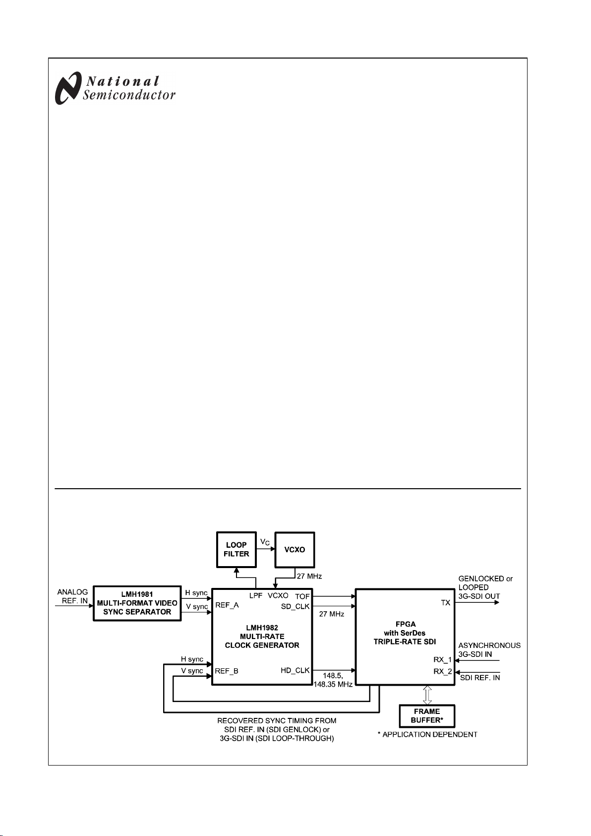
Typical System Block Diagram
30052410
© 2008 National Semiconductor Corporation 300524 www.national.com
LMH1982 Multi-Rate Video Clock Generator with Genlock
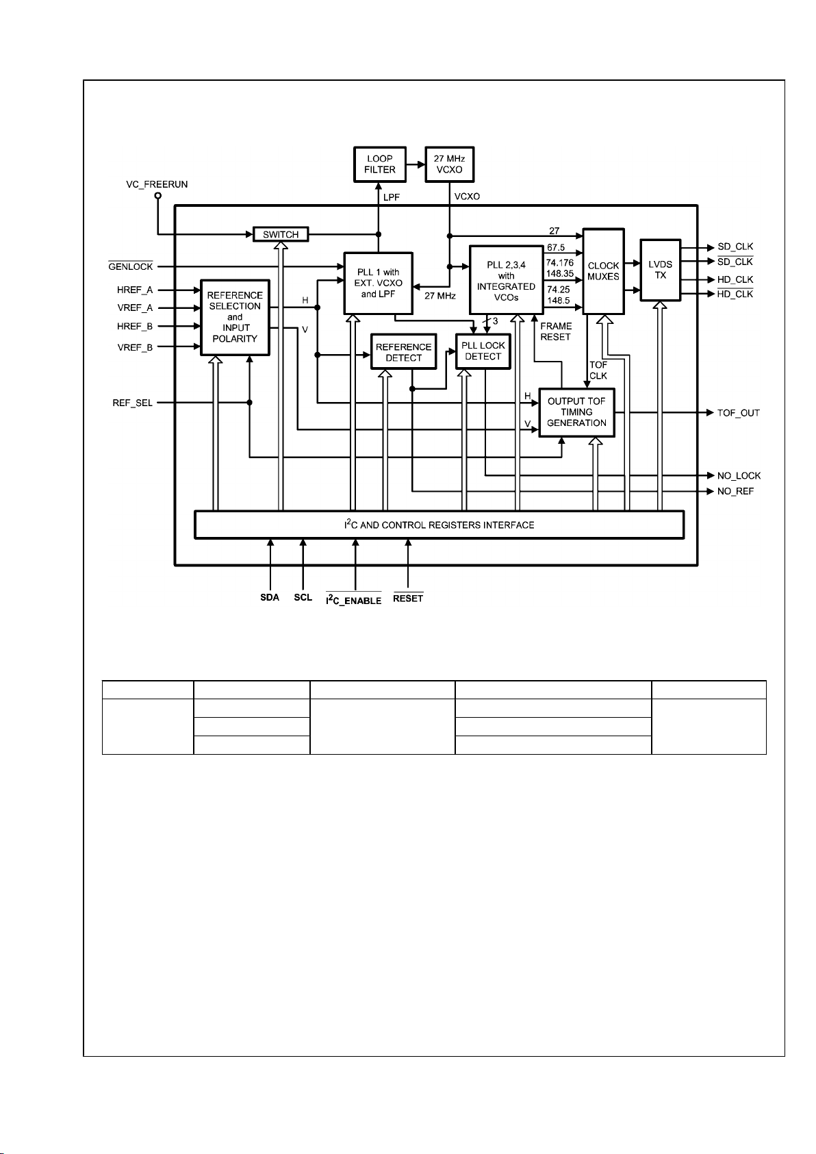
Functional Block Diagram
30052403
Ordering Information
Package Part Number Package Marking Transport Media NSC Drawing
32-Pin LLP
LMH1982SQE
L1982SQ
250 Units Tape and Reel
SQA32ALMH1982SQ 1k Units Tape and Reel
LMH1982SQX 4.5k Units Tape and Reel
www.national.com 2
LMH1982
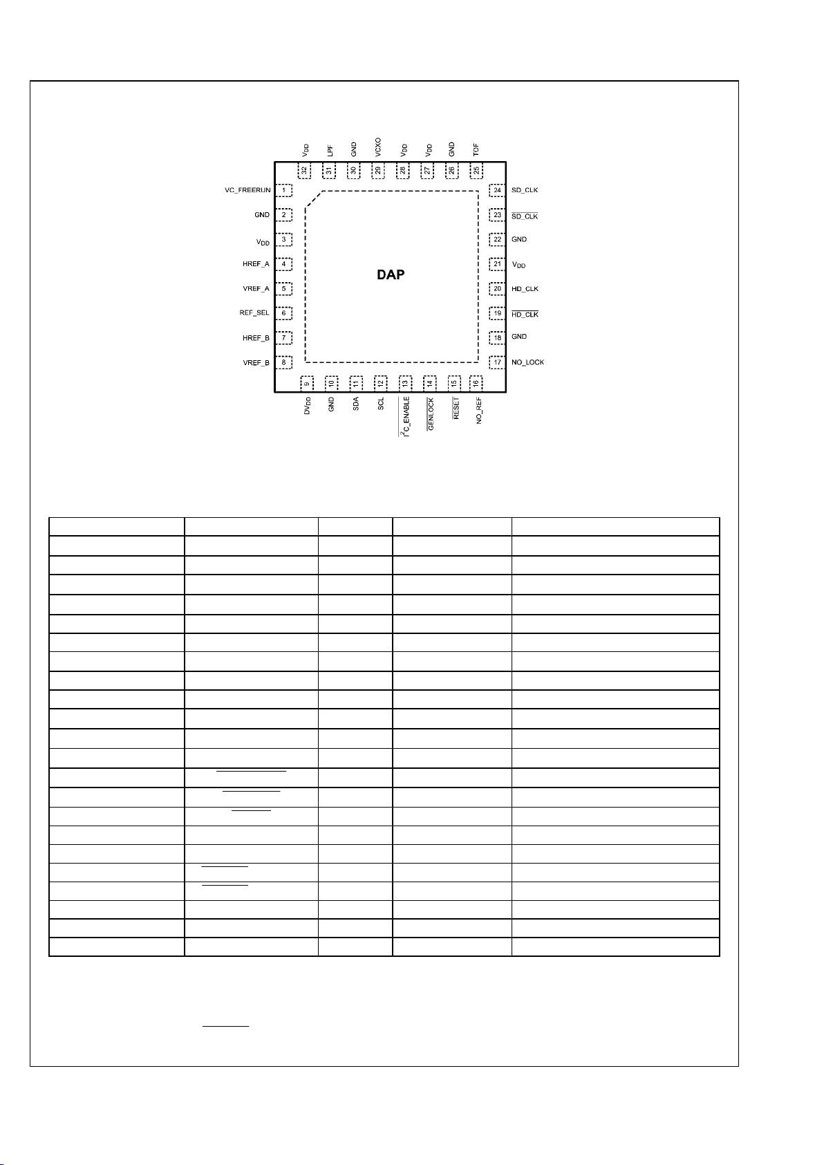
Connection Diagram
30052402
Top View
Pin Descriptions
Pin No. Pin Name I/O Signal Level Pin Description
–
DAP
–
Supply Die Attach Pad (Connect to GND)
1 VC_FREERUN I Analog Free Run Control Voltage Input
2, 10, 18, 22, 26, 30 GND
–
Supply Ground
3, 21, 27, 28, 32 V
DD
–
Supply 3.3V Supply
4 HREF_A I LVCMOS H sync Input, Reference A
5 VREF_A I LVCMOS V sync Input, Reference A
6 REF_SEL I LVCMOS Reference Select
1, 2
7 HREF_B I LVCMOS H sync Input, Reference B
8 VREF_B I LVCMOS V sync Input, Reference B
9 DV
DD
–
Supply 2.5V Supply
11 SDA I/O I2C I2C Data
3
12 SCL I I2C I2C Clock
3
13 I2C_ENABLE I LVCMOS I2C Enable
14 GENLOCK I LVCMOS Mode Select
4
15 RESET I LVCMOS Device Reset
16 NO_REF O LVCMOS Reference Status Flag
17 NO_LOCK O LVCMOS Lock Status Flag
19, 20 HD_CLK, HD_CLK O LVDS HD Clock Output
23, 24 SD_CLK, SD_CLK O LVDS SD Clock Output
25 TOF O LVCMOS Top of Frame Pulse
29 VCXO I LVCMOS VCXO Clock Input
31 LPF O Analog VCXO PLL Loop Filter
Notes
1. To control reference selection via the REF_SEL input pin instead of the I2C interface (default), program I2C_RSEL = 0 (register 00h).
2. To override reference control via pin 6 and instead use pin 6 as an logic pulse input for output alignment initialization, program PIN6_OVRD = 1 (register 02h).
Consequently, reference selection must be controlled via I2C, and the TOF_INIT bit (register 0Ah) will be ignored.
3. SDA and SCL pins each require a 4.7kΩ (typ.) pull-up resistor to the VDD supply.
4. To control mode selection via the GENLOCK input pin instead of the I2C interface (default), program I2C_GNLK = 0 (register 00h).
3 www.national.com
LMH1982

Table of Contents
General Description .............................................................................................................................. 1
Features .............................................................................................................................................. 1
Applications ......................................................................................................................................... 1
Typical System Block Diagram ............................................................................................................... 1
Functional Block Diagram ...................................................................................................................... 2
Ordering Information ............................................................................................................................. 2
Connection Diagram ............................................................................................................................. 3
Absolute Maximum Ratings .................................................................................................................... 6
Operating Ratings ................................................................................................................................ 6
Electrical Characteristics ........................................................................................................................ 6
Typical Performance Characteristics ....................................................................................................... 8
Application Information .......................................................................................................................... 9
1.0 FUNCTIONAL OVERVIEW ............................................................................................................. 9
2.0 GENERAL PROGRAMMING INFORMATION ................................................................................... 9
2.1 Recommended Start-Up Programming Sequence ............................................................................ 9
2.2 Enabling Genlock Mode ............................................................................................................... 9
2.3 Output Disturbance While Alignment Mode Enabled ......................................................................... 9
3.0 MODES OF OPERATION ............................................................................................................. 10
3.1 Free Run Mode ......................................................................................................................... 10
3.2 Genlock Mode ........................................................................................................................... 10
3.2.1 Genlock Mode State Diagram ................................................................................................. 10
3.2.2 Loss of Reference (LOR) ..................................................................................................... 10
3.2.2.1 Free Run during LOR ..................................................................................................... 10
3.2.2.2 Holdover during LOR ...................................................................................................... 10
3.3 Recognized Video Timing Formats And Standards ......................................................................... 11
4.0 INPUT REFERENCE ................................................................................................................... 13
4.1 Programming The VCXO PLL Dividers ......................................................................................... 13
4.2 Internal Reference Frame Decoder .............................................................................................. 13
5.0 OUTPUT CLOCKS AND TOF ....................................................................................................... 13
5.1 Programming The Output Clock Frequencies ................................................................................ 13
5.2 Programming The Output Timing Format ...................................................................................... 14
5.2.1 Output Clock Reference ......................................................................................................... 14
5.2.2 Output Frame Rate ............................................................................................................... 14
5.2.3 Reference Frame Rate .......................................................................................................... 14
5.2.4 Input-Output Frame Rate Ratio ............................................................................................... 14
5.2.5 Output Frame Line Offset ....................................................................................................... 14
5.3 Programming The Output Alignment Sequence ............................................................................. 15
5.3.1 Output Clock Alignment without TOF ....................................................................................... 15
5.4 Output Behavior Upon Loss Of Reference .................................................................................... 15
6.0 REFERENCE AND PLL LOCK STATUS ......................................................................................... 16
6.1 Reference Detection .................................................................................................................. 16
6.1.1 Programming the Loss of Reference (LOR) Threshold ............................................................... 16
6.2 PLL Lock Detection ................................................................................................................... 16
6.2.1 Programming the PLL Lock Threshold ..................................................................................... 16
6.2.2 PLL Lock Status Instability ..................................................................................................... 17
7.0 VCXO PLL LOOP RESPONSE .................................................................................................... 17
7.1 Loop Response Design Equations ............................................................................................... 17
7.1.1 Loop Response Optimization Tips ........................................................................................... 17
7.2 Lock Time Considerations .......................................................................................................... 18
7.3 VCXO Considerations ................................................................................................................ 18
7.4 Free Run Output Jitter ................................................................................................................ 18
8.0 I2C INTERFACE PROTOCOL ....................................................................................................... 18
8.1 Write Sequence ........................................................................................................................ 18
8.2 Read Sequence ........................................................................................................................ 18
8.3 I2C Enable Control Pin .............................................................................................................. 19
9.0 I2C INTERFACE CONTROL REGISTER DEFINITIONS ................................................................... 19
9.1 Genlock And Input Reference Control Registers ............................................................................ 20
9.2 Genlock Status And Lock Control Register .................................................................................... 20
9.3 Input Control Register ................................................................................................................ 20
9.4 PLL 1 Divider Register ............................................................................................................... 21
9.5 PLL 4 Charge Pump Current Control Registers .............................................................................. 21
9.6 Output Clock And TOF Control Register ....................................................................................... 21
9.7 TOF Configuration Registers ....................................................................................................... 21
9.8 PLL 1 Charge Pump Current Control Register ............................................................................... 22
www.national.com 4
LMH1982

9.9 PLL 2 and PLL 3 Charge Pump Current Control Register ................................................................ 23
9.10 Reserved Registers ................................................................................................................. 23
10.0 TYPICAL SYSTEM BLOCK DIAGRAMS ....................................................................................... 24
Physical Dimensions ........................................................................................................................... 26
5 www.national.com
LMH1982
Absolute Maximum Ratings (Note 1)
If Military/Aerospace specified devices are required,
please contact the National Semiconductor Sales Office/
Distributors for availability and specifications.
ESD Tolerance (Note 2)
Human Body Model 2000V
Machine Model 200V
Supply Voltage, V
DD
3.6V
Supply Voltage, DV
DD
2.75V
Input Voltage Range (any input) −0.3V to VDD +0.3V
Storage Temperature Range −65°C to +150°C
Lead Temperature (Soldering 10 sec.) 300°C
Junction Temperature, T
JMAX
150°C
Thermal Resistance (θJA)
33°C/W
Operating Ratings
V
DD
3.3V ± 5%
DV
DD
2.5V ± 5%
Input Voltage 0V to V
DD
Temperature Range, T
A
0°C to 70°C
Electrical Characteristics
Unless otherwise specified, all limits are guaranteed for TA = 25°C, VDD = 3.3V, DVDD = 2.5V, Boldface limits apply at the temperature extremes.
Symbol Parameter Conditions Min Typ Max Units
I
VDD
VDD Supply Current Default Register Values 50 mA
I
DVDD
DVDD Supply Current Default Register Values 35 mA
Free Run Voltage Control Input (Pin 1)
V
IL
Low Analog Input Voltage (Note 3) 0 V
V
IH
High Analog Input Voltage (Note 3) V
DD
V
Reference Inputs (Pins 4, 5, 7, 8)
V
IL
Low Input Voltage
IIN = ±10 μA
0 0.8 V
V
IH
High Input Voltage IIN = ±10 µA 2.0 V
DD
V
ΔT
HV
H-V Timing Offset (Note 4), Timing offset measured from H sync
to V sync pulse leading edges
2.0
μs
Digital Control Inputs (Pins 6, 13, 14, 15)
V
IL
Low Input Voltage IIN = ±10 µA 0 0.8 V
V
IH
High Input Voltage IIN = ±10 µA 2.0 V
DD
V
I2C Interface (Pins 11, 12)
V
IL
Low Input Voltage 0 0.3 V
DD
V
V
IH
High Input Voltage 0.7 V
DD
V
DD
V
I
IN
Input Current VIN between 0.1 VDD and 0.9 V
DD
−10 +10
μA
I
OL
Low Output Sink Current VOL = 0V or 0.4V 3 mA
Status Flag Outputs (Pin 16, 17)
V
OL
Low Output Voltage I
OUT
= +10 mA 0.4 V
V
OH
High Output Voltage I
OUT
= −10 mA V
DD
−0.4V
V
Top of Frame Output (Pin 25)
V
OL
Low Output Voltage I
OUT
= +10 mA 0.4 V
V
OH
High Output Voltage I
OUT
= −10 mA V
DD
−0.4V
V
I
OZ
Output Hi-Z Leakage Current TOF = Hi-Z, V
OUT
= VDD or GND 0.4 10
|μA|
t
R
Rise Time 15 pF Load 1.5 ns
t
F
Fall Time 15 pF Load 1.5 ns
t
OD
Maximum delay time from 50%
TOF_CLK active edge to 50%
TOF leading edge
Output Alignment Mode Disabled
(EN_TOF_RST = 0)
1 pixel
period
www.national.com 6
LMH1982
Clock Outputs (Pins 19, 20, 23, 24)
JitterSD27 MHz Time Interval Error
(TIE) Peak-to-Peak Output
Jitter (Note 5)
HD_CLK = Hi-Z 23 ps
27 MHz TIE Peak-to-Peak
Output Jitter(Note 5)
HD_CLK = 74.176 MHz 40 ps
67.5 MHz TIE Peak-to-Peak
Output Jitter (Note 5)
HD_CLK = 74.176 MHz 50 ps
JitterHD74.176 MHz TIE Peak-to-Peak
Output Jitter (Note 5)
SD_CLK = Hi-Z 55 ps
74.25 MHz TIE Peak-to-Peak
Output Jitter (Note 5)
SD_CLK = Hi-Z 40 ps
148.35 MHz TIE Peak-to-Peak
Output Jitter (Note 5)
SD_CLK = Hi-Z 60 ps
148.5 MHz TIE Peak-to-Peak
Output Jitter (Note 5)
SD_CLK = Hi-Z 45 ps
V
OD
Differential Signal Output
Voltage
100Ω Differential Load
247 350 454 mV
V
OS
Common Signal Output Voltage
100Ω Differential Load
1.125 1.250 1.375 V
|VOD| |Change to VOD| for
Complementary Output States
100Ω Differential Load
50 |mV|
|VOS| |Change to VOS| for
Complementary Output States
100Ω Differential Load
50 |mV|
I
OS
Output Short Circuit Current V
CLK
and V
CLK
= GND 24 |mA|
I
OZ
Output Hi-Z Leakage Current CLK = Hi-Z, V
CLK
= VDD or GND 1 10 |µA|
Note 1: Absolute Maximum Ratings are limits beyond which damage to the device may occur. Operating Ratings are conditions under which operation of the
device is intended to be functional. For guaranteed specifications and test conditions, see the Electrical Characteristics.
Note 2: Human Body Model, applicable std. MIL-STD-883, Method 3015.7. Machine Model, applicable std. JESD22-A115-A (ESD MM std. of JEDEC)
Field-Induced Charge-Device Model, applicable std. JESD22-C101-C (ESD FICDM std. of JEDEC).
Note 3: The input voltage to VC_FREERUN (pin 1) should also be within the input range of the external VCXO. The input voltage should be clean from noise
that may significantly modulate the VCXO control voltage and consequently produce output jitter during free run operation.
Note 4: ΔTHV is required specification to allow for proper frame decoding and subsequent output alignment. For interlace formats, the H-V timing offset must be
within ΔTHV for all even fields and be outside ΔTHV for odd fields. For progressive formats, the H-V timing offset must be within ΔTHV for all frames. See sections
4.2 Internal Reference Frame Decoder and 5.2.5 Output Frame Line Offset.
Note 5: The SD and HD clock output jitter is based on VCXO clock with 20 ps TIE peak-to-peak jitter. The TIE peak-to-peak jitter (typical) was measured on the
LMH1982 evaluation bench board using a Tektronix DSA70604 oscilloscope with TDSJIT3 jitter analysis software and 1 GHz differential probe.
TIE Measurement Setup: 10
-12
bit error rate (BER) and ≈1M samples recorded over multiple acquisitions. The number of acquisitions to record ≈1M samples
varied with clock frequency.
Oscilloscope Setup: 20 mV/div vertical scale, 100 us/div horizontal scale, and 25 Gs/s sampling rate.
7 www.national.com
LMH1982
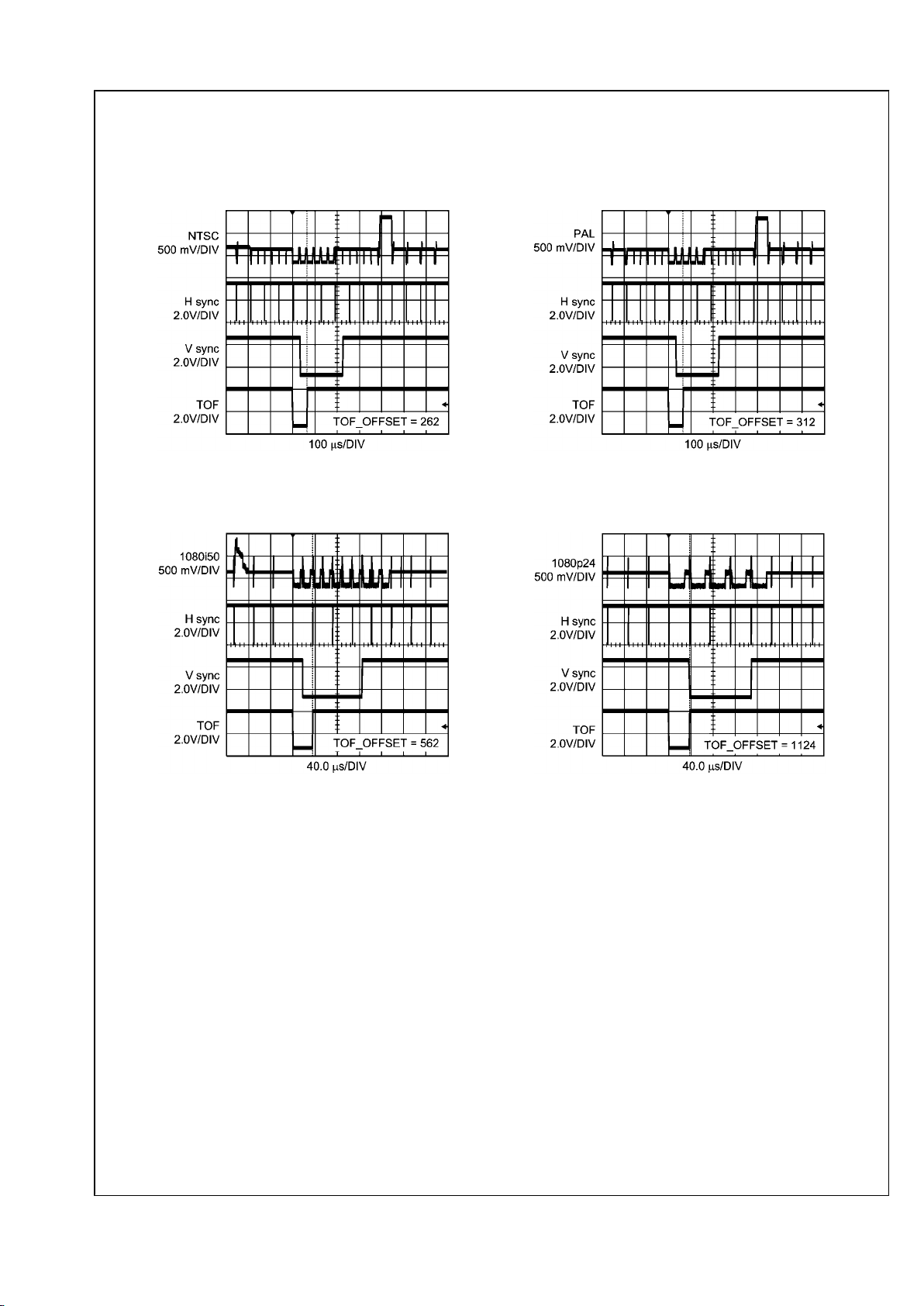
Typical Performance Characteristics
Note:
Test conditions: VDD = 3.3V, D
VDD
= 2.5V, analog video reference from Tektronix TG700 AVG7 (SD video module) and AWVG7 (HD video module),
H sync and V sync inputs from the LMH1981.
NTSC TOF Pulse
30052433
PAL TOF Pulse
30052434
1080i50 TOF Pulse
30052435
1080p24 TOF Pulse
30052432
www.national.com 8
LMH1982
Application Information
1.0 FUNCTIONAL OVERVIEW
The LMH1982 is an analog phase locked loop (PLL) clock
generator that can output simultaneous SD and HD video
clocks synchronized or “genlocked” to H sync and V sync input reference timing. The LMH1982 features an output Top of
Frame (TOF) pulse generator with programmable timing that
can also be synchronized to the reference frame. Two reference ports are provided to allow a secondary input to be
selected.
The clock generator uses a two-stage PLL architecture. The
first stage is a VCXO-based PLL (PLL 1) that requires an external 27 MHz VCXO and loop filter. In Genlock mode, PLL 1
can phase lock the VCXO clock to the input reference after
programming the PLL divider ratio. The use of a VCXO provides a low phase noise clock source even when the
LMH1982 is configured with a low loop bandwidth, which is
necessary to attenuate input timing jitter for minimum jitter
transfer. The combination of the external VCXO, external loop
filter, and programmable PLL parameters can provide flexibility for the system designer to optimize the loop bandwidth
and loop response for the application.
The second stage consists of three PLLs (PLL 2, 3, 4) with
integrated VCOs and loop filters. These PLLs will attempt to
continually track the reference VCXO clock phase from
PLL 1 regardless of the device mode. The second stage PLLs
have pre-configured divider ratios to provide frequency multiplication or translation from the VCXO clock frequency. The
VCO PLLs use a high loop bandwidth to assure PLL stability,
so the VCXO must provide a stable low-jitter clock reference
to ensure optimal output jitter performance.
Any unused clock output can be put in Hi-Z mode, which can
be useful for reducing power dissipation as well as reducing
jitter or phase noise on the active clock output.
The TOF pulse can be programmed to indicate the start (top)
of frame and even provide format cross-locking. The output
format registers should be programmed to specify the output
timing format, the output timing offset relative to the reference,
and the initial alignment of reference clock and TOF pulse to
the reference frame. If unused, the TOF output can also be
put in Hi-Z mode.
When a loss of reference occurs during genlock, PLL 1 can
default to either Free run or Holdover operation. When free
run is selected, the output frequency accuracy will be determined by the external bias on the free run control voltage input
pin, VC_FREERUN. When Holdover is selected, the loop filter
can hold the control voltage to maintain short-term output
phase accuracy for a brief period in order to allow the application to select the secondary input reference and re-lock the
outputs. These options in combination with proper PLL 1 loop
response design can provide flexibility to manage output
clock behavior during loss and re-acquisition of the reference.
The reference status and PLL lock status flags can provide
real-time status indication to the application system. The loss
of reference and lock detection thresholds can also be configured.
TABLE 1. LMH1982 PLL and Clock Summary
PLL Input Reference Divider Ratio (reduced) Output Clock
Frequency (MHz)
Output Port
PLL 1 H sync Programmable 27 SD_CLK
PLL 2 VCXO clock 11/4 or 11/2 74.25 or 148.5 HD_CLK
PLL 3 VCXO clock 250/91 or 500/91
74.25/1.001 (74.176) or
148.5/1.001 (148.35) HD_CLK
PLL 4 VCXO clock 5/2 67.5 SD_CLK
2.0 GENERAL PROGRAMMING INFORMATION
The LMH1982 can be configured by programming the control
registers via the I2C interface. The I2C_ENABLE
pin must be
set low or tied to GND to allow I2C communication; otherwise,
the LMH1982 will not acknowledge communication. The I2C
slave addresses are DCh for write sequences and DDh for
read sequences. See section 8.0 I2C INTERFACE PROTO-
COL and 9.0 I2C INTERFACE CONTROL REGISTER DEFINITIONS.
2.1 Recommended Start-Up Programming Sequence
The following programming sequence is necessary to ensure
proper operation of the 148.35 MHz output clock following any
power-up or reset condition. This sequence is also necessary
after changing from any other HD clock frequency or Hi-Z
mode.
1.
Program HD_FREQ = 11b and HD_HIZ = 0 (register 08h)
to select and enable the 148.35 MHz HD clock.
2.
Program a value of 1 to the following register parameters:
—
FB_DIV = 1 (register 04h-05h)
—
TOF_RST = 1 (register 09h-0Ah)
—
REF_LPFM = 1 (register 0Dh-0Eh)
—
EN_TOF_RST = 1 (register 0Ah)
3.
Wait at least 1 period of the 27 MHz VCXO clock.
4.
Program EN_TOF_RST = 0.
Once this sequence is completed, the 148.35 MHz clock will
operate correctly and normal device configuration can resume. Otherwise, the 148.35 MHz clock may have glitches or
errors until the internal counters of PLL 3 are reset by the
programming sequence above. All other output clocks do not
require this reset sequence for proper operation.
2.2 Enabling Genlock Mode
Upon device power up or reset, the default mode of operation
is Free Run mode. To enable Genlock mode, set GNLK = 1
(register 00h). Refer to section 3.2 Genlock Mode.
2.3 Output Disturbance While Alignment Mode Enabled
While the output alignment mode is enabled (EN_TOF_RST
= 1) and maintained beyond the initial alignment (initialization), the output signals can be abruptly phase-aligned to the
reference on every output frame. Continual alignment can
cause excessive phase “jumps” or jitter on the output clock
edge coinciding with the TOF pulse; this effect is unavoidable
and can be caused by slight differences in the internal counter
reset timing for the TOF generation and large input jitter. The
characteristic of the output jitter can also vary in severity from
process variation, part variation, and the selected clock reference frequency. . This output jitter can only be inhibited by
9 www.national.com
LMH1982
 Loading...