

NSC LMH0341SQX, LMH0341 Datasheet
ADVANCE INFORMATION
June 2007
LMH0341, LMH0041, LMH0071, LMH0051
3G, HD, SD, DVB-ASI SDI Deserializer with Loopthrough
and LVDS Interface
General Description
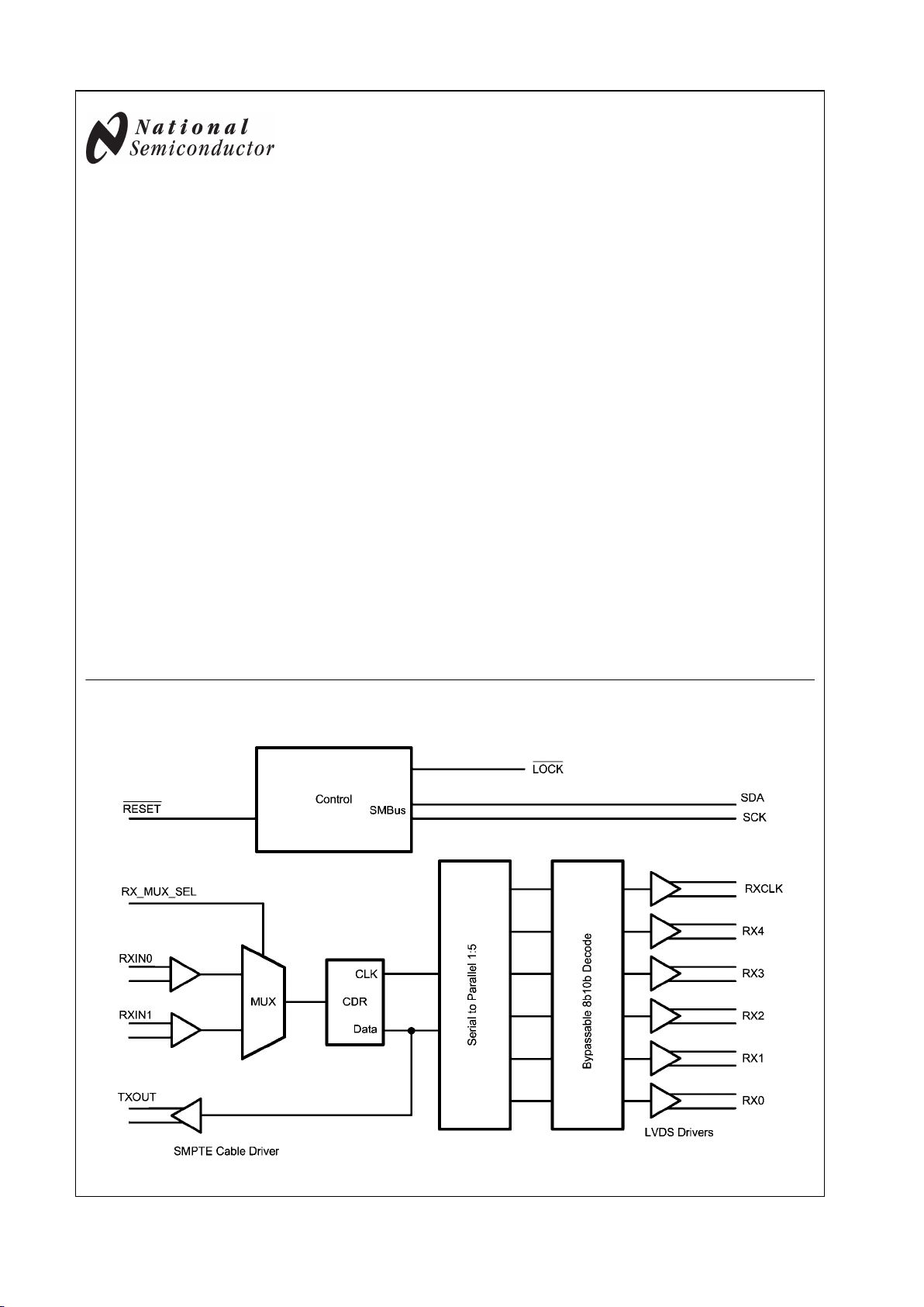
The LMH0041 family of products provide a very simple 1:5
deserializer and receiver function. The device is intended to
be paired with an FPGA host which will receive the raw 5 bit
data words and will decode the data appropriately such that
a SMPTE standard signal may be recovered. The devices are
designed to receive data compliant with DVB-ASI, SMPTE
259M, SMPTE 292M and/or SMPTE 424M. The interface between the LMH0041 and the FPGA consists of a 5 bit wide
LVDS bus, an LVDS clock and an SMBus interface. All devices except for the LMH0051 includes a reclocked
feedthrough output with a SMPTE compliant cable driver. The
LMH0341 includes support for SMPTE424M, and the
LMH0071 is a Stadard Definition (SD) only variant. The product is packaged in a physically small 48 pin LLP package.
Key Specifications
■
Output compliant with SMPTE 259M-C, SMPTE 292M,
SMPTE 424M and DVB-ASI
■
Typical power dissipation: 410 mW (loopthrough disabled)
■
0.6 UI Input Jitter Tolerance
Features
■
LVDS Interface
■
Dual multiplexed inputs
■
No external VCO or clock required
■
Loopthrough with Cable Driver
■
SMBus configuration interface
■
48 pin LLP package
Applications
■
SDI interfaces for:
—
Video Cameras
—
DVRs
—
Video Switchers
—
Video Editing Systems
Block Diagram
30017201
© 2007 National Semiconductor Corporation 300172 www.national.com
LMH0341, LMH0041, LMH0071, LMH0051 3G, HD, SD, DVB-ASI SDI Deserializer with
Loopthrough and LVDS Interface
TABLE 1. Feature Table
Device SMPTE 424M Support SMPTE 292M Support SMPTE 259M Support DVB-ASI Support Active Loopthrough
LMH0341
× × × × ×
LMH0041
× × × ×
LMH0071
× × ×
LMH0051
× × ×
www.national.com 2
LMH0341, LMH0041, LMH0071, LMH0051
Absolute Maximum Ratings (Note 1)
If Military/Aerospace specified devices are required,
please contact the National Semiconductor Sales Office/
Distributors for availability and specifications.
Supply Voltage (VCC)
−0.3V to +4.0V
LVCMOS (SMBus) input voltage −0.3V to (VCC+0.3V)
LVCMOS (SMBus) output voltage −0.3V to (VCC+0.3V)
LVDS Input Voltage 0.3V to 3.6V
Junction Temperature +150°C
Storage Temperature −65° to 150°C
Lead Temperature—Soldering 4 seconds +260°C
Thermal Resistance—
Junction to Ambient—θ
JA
40°C/W
ESD Rating—Human Body Model,
1.5 KΩ, 100 pF 4KV
Recommended Operating Conditions
Parameter Min Typ Max Units
Supply Voltage (VCC-GND) 3.1 3.3 3.5 V
2.4 2.5 2.6 V
Supply noise amplitude (10 Hz to 50 MHz) 100 mV
P-P
Ambient Temperature −40 +25 +85 °C
Case Temperature 100 °C
LVDS PCB board trace length (mismatch <2%) 25 cm
LMH0041 Electrical Characteristics Over supply and Operating Temperature ranges unless otherwise
specified
Symbol Parameter Condition Min
Typ
(Note 2)
Max Units
I
DD2.5
2.5V supply current mA
I
DD3.3
3.3V supply current 106 mA
P
D
Power Consumption VDD = 3.6V All outputs
terminated by 100Ω, 2.97 Gbps
output, loopthrough disabled
410 mW
Loopthrough enabled 475 mW
Control Pin Electrical Characteristics Over supply and Operating Temperature ranges unless otherwise
specified. Applies to MODE0, MODE1, RESET and LOCK
Symbol Parameter Condition Min
Typ
(Note 2)
Max Units
V
IH
High Level Input Voltage 2.0 VCC +0.3 V
V
IL
Low Level Input Voltage −0.3 0.8 V
V
OH
High Level Output Voltage IOH = −0.4 mA 2.7 3.3 V
IOH = −2 mA 2.7 2.85 V
V
OL
Low Level Output Voltage IOL = 2 mA 0.1 0.3 V
V
CL
Input Clamp Voltage ICL = −18 mA −0.79 −1.5 V
I
IN
Input Current VIN = 0.4V, 2.5V or V
DD
1.8 15
μA
VIN = GND −15 0
μA
I
OS
Output Short Circuit Current V
OUT
= 0V −120 mA
3 www.national.com
LMH0341, LMH0041, LMH0071, LMH0051
LVDS Output Electrical Characteristics Over supply and Operating Temperature ranges unless
otherwise specified
Symbol Parameter Condition Min
Typ
(Note 2)
Max Units
V
OD
Differential Output Voltage
RL = 100Ω
250 345 459 mV
ΔV
OD
Change in VOD between
complementary output states
35 mV
V
OS
Offset Voltage 1.125 1.25 1.375 V
ΔV
OS
Change in VOS between
complementary output states
35 mV
I
OS
Output Short Circuit Current
V
OUT
= 0V, RL = 100Ω
50 mA
I
OZ
Output TRI-state current PD = 0V, V
OUT
= 0V or V
CC
±1 ±10
μA
SMBus Input Electrical Characteristics Over supply and Operating Temperature ranges unless
otherwise specified
Symbol Parameter Condition Min
Typ
(Note 2)
Max Units
V
SIL
Data, Clock Input Low Voltage 0.8 V
V
SIH
Data, Clock Input High Voltage 2.1 V
SDD
V
I
SPULLUP
Current through pull-up resistor or
current source
4 mA
V
SDD
Nominal Bus Voltage 2.375 3.6 V
I
SLEAKB
Input Leakage per bus segment See (Note 3) −200 200
μA
I
SLEAKP
Input Leakage per pin −10 10
μA
C
SI
Capacitance for SMBdata and
SMBclk
See (Notes 3, 4) 10 pF
R
STERM
Termination Resistance V
SDD3.3
See (Notes 3, 4, 5) 2000
Ω
V
SDD3.3
See (Notes 3, 4, 5) 1000
Ω
LVDS Switching Characteristics
Symbol Parameter Condition Min
Typ
(Note 2)
Max Units
t
ROTR
LVDS Low to High Transition time See Figure 1 LVDS Switching
times
0.2T 3 ns
t
ROTF
LVDS High to Low Transition time 0.2T 3 ns
t
ROCP
Receiver output clock period RxCLKOUT is DDR. If divide by
4 is enabled, the output clock
period will be doubled
3.2 2T 8,37 ns
t
RODC
RxCLKOUT Duty Cycle 45 50 55 %
t
ROCH
RxCLKOUT high time See Figure 2 Receiver timing
specifications
1.44 ns
t
ROCL
RxCLKOUT low time 1.44 ns
t
RBIT
Receiver output bit width T ns
t
ROSC
RxOUT Seup to RxCLKOUT OUT See Figure 2 Receiver timing
specifications
200 ps
t
ROHC
RxOUT Hold to RxCLKOUT OUT 200 ps
t
ROJR
Receiver output Random Jitter Receiver output intrinsic
random jitter.
Bit error rate ≤ 10
-15
. Alternating
10 pattern. RMS
2 ps
t
ROJT
Peak-to-Peak Receiver Output Jitter 200 ps
TOL
JIT
Receiver Jitter Tolerance See (Note 6) 0.6 UI
P-P
t
RD
Receiver Propagation Delay See Figure 3 Receiver (LVDS
Interface) Propagation Delay
4*t
RBIT
+TBD
4*t
RBIT
+TBD
4*t
RBIT
+TBD
ns
www.national.com 4
LMH0341, LMH0041, LMH0071, LMH0051
 Loading...