NSC LMH0340, LMH0340SQX Datasheet
PRELIMINARY
April 10, 2008
LMH0340, LMH0040, LMH0070, LMH0050
3 Gbps, HD, SD, DVB-ASI SDI Serializer and Cable Driver
with LVDS Interface
General Description
The LMH0340 3 Gbps SDI Serializer is part of National’s family of FPGA-Attach SER/DES products supporting 5-bit LVDS
interfaces with FPGAs. An FPGA Host will format data with
supplied IP such that the output of the LMH0340 is compliant
with the requirements of DVB-ASI, SMPTE 259M-C, SMPTE
292M and SMPTE 424M standards.
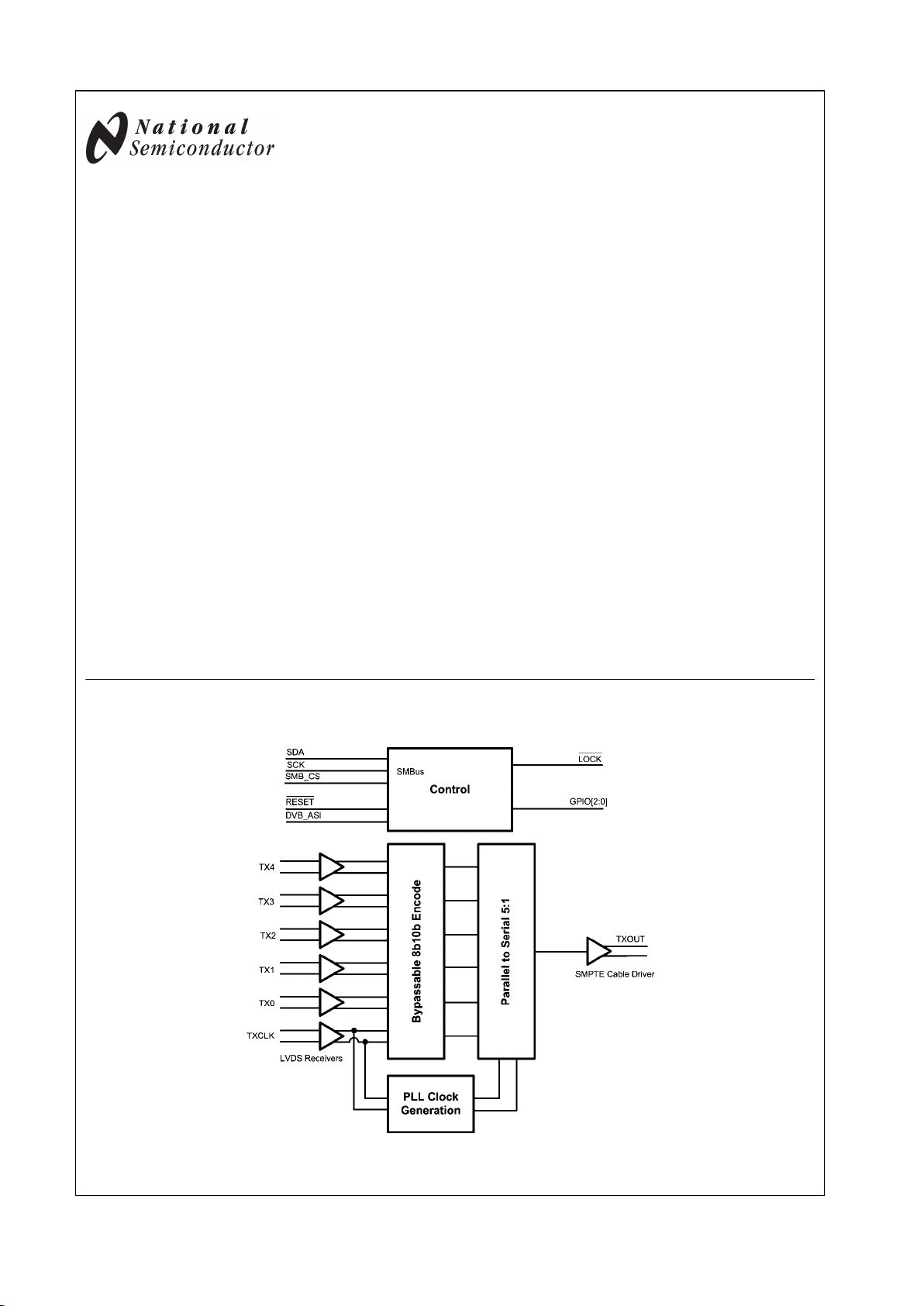
The interface between the SER (Serializer) and the FPGA
consists of a 5 bit wide LVDS data bus, an LVDS clock and
an SMBus interface. The LMH0340 / LMH0040 / LMH0070
SER devices include an integrated cable driver which is fully
compliant with all of the SMPTE specifications listed above.
Refer to Table 1 for a complete listing of single channel serializers currently offered in this family. The LMH0050 has a
CML output driver that can drive a differential transmission
line or interface to a cable driver.
The FPGA-Attach SER/DES family is supported by a suite of
IP which allows the design engineer to quickly develop video
applications using the SER/DES products. The SER is packaged in a physically small 48 pin LLP package.
Key Specifications
■
Output compliant with SMPTE 424M, SMPTE 292M,
SMPTE 259M-C and DVB-ASI
■
Typical power dissipation: 440 mW
■
30 ps typical output jitter (HD, 3G)
Features
■
LVDS Interface to Host FPGA
■
No external VCO or clock ref required
■
Integrated Variable Output Cable Driver
■
3.3V SMBus configuration interface
■
Integrated TXCLK PLL cleans clock noise
■
Small 48pin LLP package
Applications
■
SDI interfaces for:
—
Video Cameras
—
DVRs
—
Video Switchers
—
Video Editing Systems
General Block Diagram
30017001
TRI-STATE® is a registered trademark of National Semiconductor Corporation.
© 2008 National Semiconductor Corporation 300170 www.national.com
LMH0340, LMH0040, LMH0070, LMH0050 3Gbps, HD, SD, DVB-ASI SDI Serializer and Cable
Driver with LVDS Interface

Pin Descriptions
Pin Name Type Description
LVDS Input Interface
TX[4:0]+
TX[4:0]-
Input, LVDS LVDS Data Input Pins
Five channel wide DDR interface. Internal 100Ω termination.
TXCLK+
TXCLK-
Input, LVDS LVDS Clock Input Pins
DDR Interface. Internal 100Ω termination.
Serial Output Interface
TXOUT+ Output, CML Serial Digital Interface Output Pin
Non-Inverting Output
TXOUT- Output, CML Serial Digital Interface Output Pin
Inverting Output
SMBus Interface
SDA I/O, LVCMOS SMBus Data I/O Pin
SCK Input, LVCMOS SMBus Clock Input Pin
SMB_CS Input, LVCMOS SMBus Chip Select Input Pin
Device is selected when High.
Control and Configuration Pins
RESET Input, LVCMOS Reset Input Pin
H = normal mode
L = device in RESET
LOCK Output, LVCMOS PLL LOCK Status Output
H = unlock condition
L = Device is Locked
DVB_ASI Input, LVCMOS DVB_ASI Select Input
H = DVB_ASI Mode enabled
L = Normal Mode enabled
GPIO[2:0] I/O, LVCMOS General Purpose Input / Output
Software configurable I/O pins.
RSVD_H Input, LVCMOS Configuration Input – Must tie High
Pull High via 5 kΩ resistor to V
DD3V3
Analog Inputs
R
SET
Input, analog Serial Output Amplitude Control
Resistor connected from this pin to ground to set the signal amplitude. Nominally
8.06kΩ for 800mV output (SMPTE).
LF_CP Input, analog Loop Filter Connection
LF_REF Input, analog Loop Filter Reference
DNC Do Not Connect – Leave Open
Power Supply and Ground
V
DD3V3
Power 3.3V Power Supply connection
V
DDPLL
Power 3.3V PLL Power Supply connection
V
DD2V5
Power 2.5V Power Supply connection
GND Ground Ground connection – The DAP (large center pad) is the primary GND connection
for the device and must be connected to Ground along with the GND pins.
TABLE 1. Feature Table
Device
SMPTE 424M
Support (3G)
SMPTE 292M
Support (HD)
SMPTE 259M
Support (SD)
DVB-ASI
Support
SMPTE compliant
Cable Driver
LMH0340 X X X X X
LMH0040 X X X X
LMH0070 X X X
LMH0050 X X X
www.national.com 2
LMH0340, LMH0040, LMH0070, LMH0050
Absolute Maximum Ratings (Note 1)
If Military/Aerospace specified devices are required,
please contact the National Semiconductor Sales Office/
Distributors for availability and specifications.
Supply Voltage (V
DD3V3
) −0.3V to +4.0V
Supply Voltage (V
DD2V5
) −0.3V to +3.0V
LVCMOS input voltage −0.3V to (V
DD3V3
+0.3V)
LVCMOS output voltage −0.3V to (V
DD3V3
+0.3V)
SMBus I/O voltage -0.3V to +3.6V
LVDS Input Voltage -0.3V to +3.6V
Junction Temperature +150°C
Storage Temperature −65° to 150°C
Thermal Resistance—
Junction to Ambient—θ
JA
25°C/W
ESD Rating—Human Body Model,
1.5 KΩ, 100 pF
≥±8kV
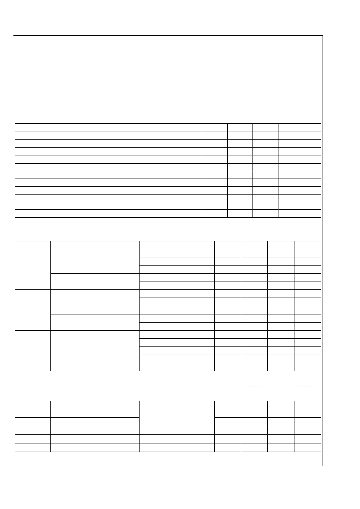
Recommended Operating Conditions
Parameter Min Typ Max Units
Supply Voltage (V
DD3V3
-GND) 3.135 3.3 3.465 V
Supply Voltage (V
DD2V5
-GND) 2.375 2.5 2.625 V
Supply noise amplitude (10 Hz to 50 MHz) 100 mV
P-P
Ambient Temperature −40 +25 +85 °C
Case Temperature 100 °C
TXCLK input frequency – LMH0340 27 297 MHz
TXCLK input frequency – LMH0040 27 149 MHz
TXCLK input frequency – LMH0070 26.5 27 28 MHz
TXCLK input frequency – LMH0050 27 149 MHz
LVDS PCB board trace length (mismatch <2%) 25 cm
Output Driver Pullup Resistor Termination Voltage (Note 10) 2.5 2.625 V
Electrical Characteristics
Over supply and Operating Temperature ranges unless otherwise specified. (Note 2)
Symbol Parameter Condition Min Typ Max Units
I
DD2.5
2.5V supply current for LMH0340,
LMH0040, or LMH0070
2.97 Gbps 93 102 mA
1.485 Gbps 80 87 mA
270 Mbps 63 69 mA
2.5V supply current for LMH0050 1.485 Gbps 87 95 mA
270 Mbps 70 75 mA
I
DD3.3
3.3V supply current for LMH0340,
LMH0040, or LMH0070
2.97 Gbps 73 85 mA
1.485 Gbps 73 85 mA
270 Mbps 73 85 mA
3.3V supply current for LMH0050 1.485 Gbps 73 85 mA
270 Mbps 73 85 mA
PD Power Consumption LMH0340 - 2.97 Gbps 475 545 mW
LMH0040 - 1.485 Gbps 440 510 mW
LMH0050 - 1.485 Gbps 460 525 mW
LMH0050 - 270 Mbps 415 485 mW
LMH0070 - 270 Mbps 400 470 mW
Control Pin Electrical Characteristics
Over supply and Operating Temperature ranges unless otherwise specified. Applies to DVB_ASI, RESET
, GPIO[2:0] and LOCK.
(Note 2)
Symbol Parameter Condition Min Typ Max Units
V
IH
High Level Input Voltage 2.0 V
DD3V3
V
V
IL
Low Level Input Voltage 0 0.8 V
V
OH
High Level Output Voltage IOH=−2 mA 2.7 3.3 V
V
OL
Low Level Output Voltage IOL=2 mA 0.3 V
V
CL
Input Clamp Voltage ICL=−18 mA -0.79 -1.5 V
3 www.national.com
LMH0340, LMH0040, LMH0070, LMH0050
Symbol Parameter Condition Min Typ Max Units
I
IN
Input Current VIN=0.4V, 2.5V or V
DD
-35 35
μA
I
OS
Output Short Circuit Current V
OUT
=0V -40 mA
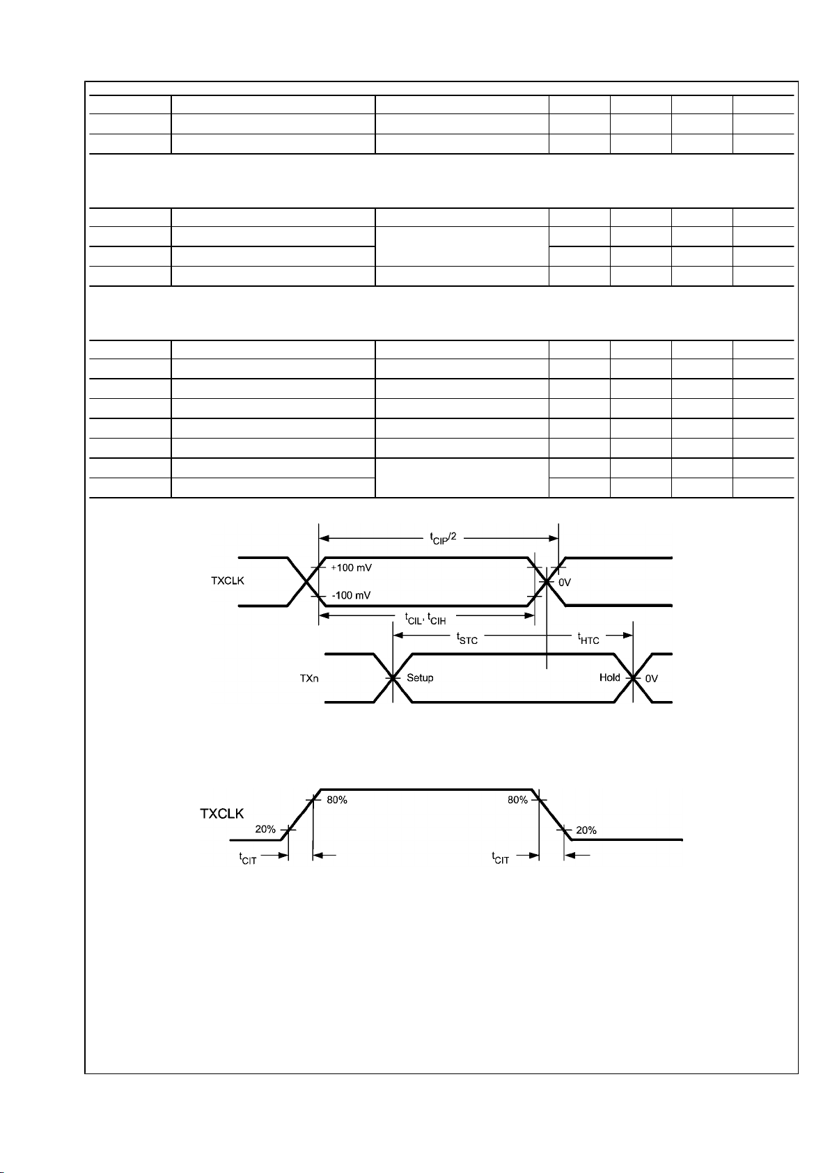
LVDS Input Electrical Characteristics
Over supply and Operating Temperature ranges unless otherwise specified. (Note 2)
Symbol Parameter Condition Min Typ Max Units
V
TH
Differential Input High threshold 0.05V<VCM<2.4V +100 mV
V
TL
Differential Input Low threshold −100 mV
R
LVIN
Input Impedance Measured between LVDS pairs 85 100 115
Ω
LVDS Switching Characteristics
Over supply and Operating Temperature ranges unless otherwise specified. (Note 2)
Symbol Parameter Condition Min Typ Max Units
t
CIP
TxCLKIN Period See Figure 1 3.2 2T 37 ns
t
CIT
TxCLKIN Transition Time See Figure 2 0.5 1.0 3.0 ns
t
CIH
TxCLKIN IN High Time See Figure 1 0.7T T 1.3T ns
t
CIL
TxCLKIN IN Low Time See Figure 1 0.7T T 1.3T ns
t
XIT
TxIN Transition Time 0.15 3 ns
t
STC
TxIN Setup to TxCLKIN See Figure 1, (Note 11) -550 ps
t
HTC
TxIN Hold to TxCLKIN 900 ps
30017002
FIGURE 1. LVDS Input Timing Diagram
30017003
FIGURE 2. Transmit Clock Transition Times
www.national.com 4
LMH0340, LMH0040, LMH0070, LMH0050
SMBus Input Electrical Characteristics
Over supply and Operating Temperature ranges unless otherwise specified. (Note 2)
Symbol Parameter Condition Min Typ Max Units
V
SIL
Data, Clock Input Low Voltage 0.8 V
V
SIH
Data, Clock Input High Voltage 2 V
SDD
V
I
SPULLUP
Current through pull-up resistor or
current source
(Note 3) 4 mA
V
SDD
Nominal Bus Voltage 2.375 3.6 V
I
SLEAKB
Input Leakage per bus segment (Note 3) −200 200
μA
I
SLEAKP
Input Leakage per pin −10 10
μA
C
SI
Capacitance for SMBdata and
SMBclk
(Notes 3, 4) 10 pF
R
STERM
Termination Resistance V
SDD3V3
(Notes 5, 4, 3) 1000
Ω
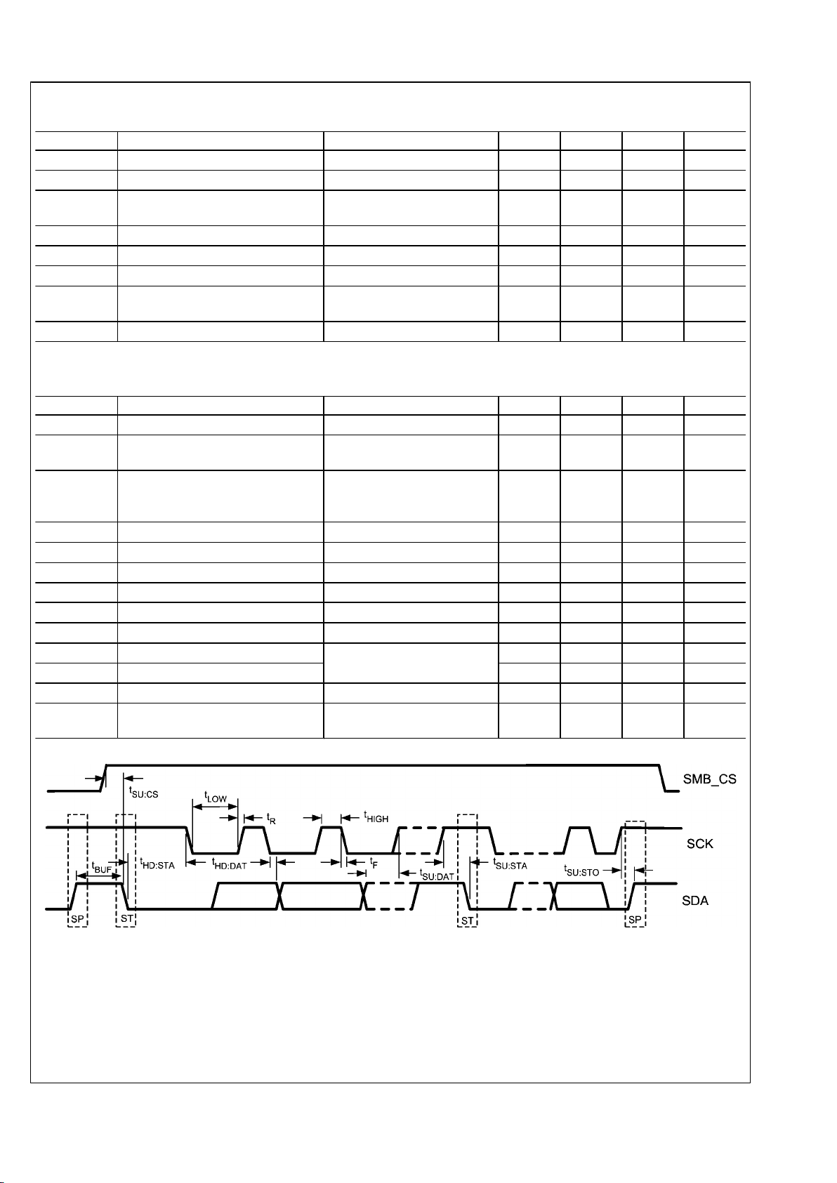
SMBus Switching Characteristics
Over supply and Operating Temperature ranges unless otherwise specified. (Note 2)
Symbol Parameter Condition Min Typ Max Units
f
SMB
Bus Operating Frequency 10 100 kHz
t
BUF
Bus free time between stop and start
condition
4.7
μs
t
HD:STA
Hold time after (repeated) start
condition. After this period, the first
clock is generated
At I
SPULLUP
= MAX 4.0
μs
t
SU:STA
Repeated Start condition setup time 4.7
μs
t
SU:STO
Stop Condition setup time 4.0
μs
t
HD:DAT
Data hold time 300 ns
t
SU:DAT
Data setup time 250 ns
t
LOW
Clock Low Time 4.7
μs
t
HIGH
Clock High Time 4.0 50
μs
t
F
Clock/data fall time 20% to 80% 300 ns
t
R
Clock/data rise time 1000 ns
t
SU:CS
SMB_CS setup time 30 ns
t
POR
Time in which a device must be
operational after power on
500 ms
30017004
(levels are V
SIL
and V
SIH
)
FIGURE 3. SMBus Timing Parameters
5 www.national.com
LMH0340, LMH0040, LMH0070, LMH0050
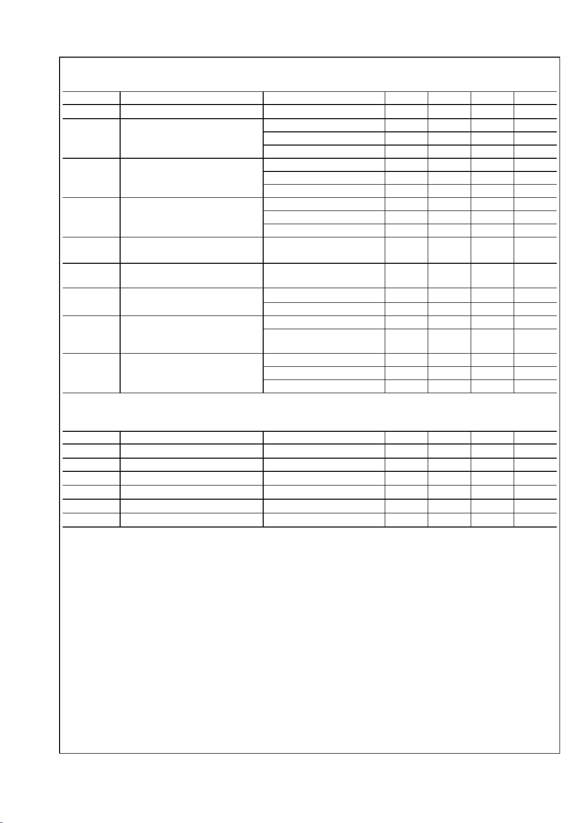
SDI Output Characteristics — LMH0340 / LMH0040 / LMH0070
Over supply and Operating Temperature ranges unless otherwise specified. (Note 2)
Symbol Parameter Condition Min Typ Max Units
V
OD
SDI Output Voltage
into 75Ω load
720 800 880 mV
DR SDI Output Datarate LMH0340 270 2,970 Mbps
LMH0040 270 1,485 Mbps
LMH0070 270 Mbps
t
r
SDI Output Rise Time 2.97 Gbps 90 135 ps
1.485 Gbps 90 220 ps
<1.485 Gbps 400 700 1000 ps
t
f
SDI Output Fall Time 2.97 Gbps 90 135 ps
1.485 Gbps 90 220 ps
<1.485 Gbps 400 700 1000 ps
Δt
t
Mismatch between rise and fall time
≥1.485 Gbps
(Note 9)
30 ps
t
SD
Propagation Delay Latency See Figure 4 9.5 TXCLK
cycle
t
J
Peak to Peak Alignment Jitter
≥1.485 Gbps(Note 6)
30 50 ps
270 Mbps(Note 6) 100 200 ps
RL Output Return Loss — EVK
Specification
(Note 12)
Measured 5 MHz to 1485 MHz 15 20 dB
Measured 1485 MHz to 2970
MHz
10 15 dB
t
OS
Output Overshoot
(Note 9)
2.97 Gbps 8 %
1.485 Gbps 5 %
270 Mbps 2 %
CML Output Characteristics — LMH0050
Over supply and Operating Temperature ranges unless otherwise specified. (Note 2)
Symbol Parameter Condition Min Typ Max Units
V
OD
Output Voltage
into 100 Ω differential load
1175 1450 mV
DR Data Rate 270 1485 Mbps
t
r
Output Rise Time 100 ps
t
f
Output Fall Time 100 ps
t
J
Peak-to-Peak Alignment Jitter 1.485 Gbps 25 50 ps
R
OUT
Output Termination Resistance Output Pin to V
DD2V5
Pin 40 50 60
Ω
www.national.com 6
LMH0340, LMH0040, LMH0070, LMH0050
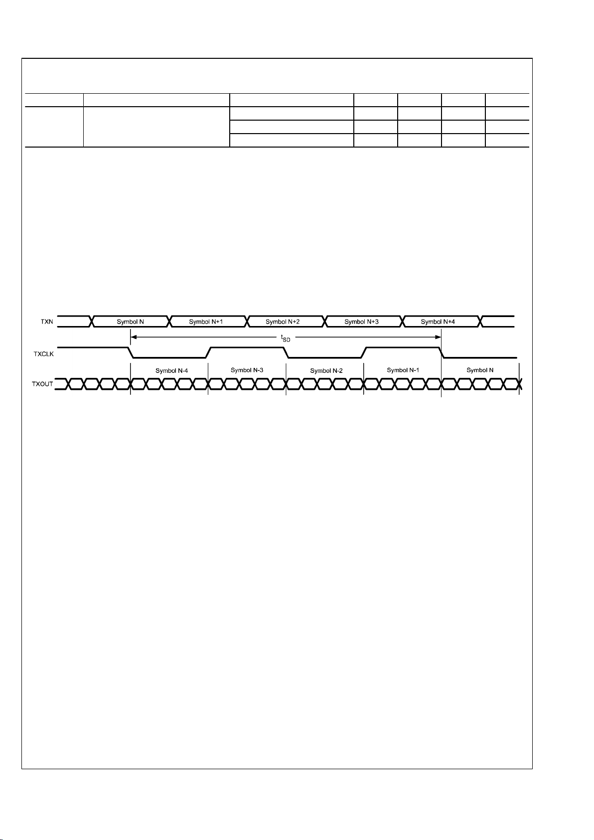
Device Switching Characteristics
Over supply and Operating Temperature ranges unless otherwise specified. (Note 2)
Symbol Parameter Condition Min Typ Max Units
t
TPLD
Device Lock Time 2.97 Gbps 10 ms
1.485 Gbps 11 ms
270 Mbps 15 ms
Note 1: “Absolute Maximum Ratings” are limits beyond which the safety of the device cannot be guaranteed. It is not implied that the device will operate up to
these limits.
Note 2: Typical Parameters measured at V
DD3V3
=3.3V, V
DD2V5
=2.5V, TA=25°C. They are for reference purposes and are not production tested.
Note 3: Recommended value—Parameter is not tested.
Note 4: Recommended maximum capacitance load per bus segment is 400 pF.
Note 5: Maximum termination voltage should be identical to the device supply voltage.
Note 6: Measured in accordance with SMPTE RP184. 100% production tested.
Note 7: Register 0x30'h bits [7:5] is at default value of 011'b
Note 8: Measured with R
SET
= 8.06 kΩ and register 0x69'h at default value.
Note 9: Specification guaranteed by characterization.
Note 10: Applies to LMH0340, LMH0040, and LMH0070.
Note 11: Parameter uses default settings in registers: 0x24'h and 0x30'h.
Note 12: Output Return Loss specification applies to measurement on the EVK PCB (LMH0340 ALP Daughter Card) per SMPTE requirements.
30017005
FIGURE 4. LVDS Interface Propagation Delay
7 www.national.com
LMH0340, LMH0040, LMH0070, LMH0050
 Loading...