NSC LMF90CCWMX, LMF90CCWM Datasheet
TL/H/10354
LMF90 4th-Order Elliptic Notch Filter
December 1994
LMF90
4th-Order Elliptic Notch Filter
General Description
The LMF90 is a fourth-order elliptic notch (band-reject) filter
based on switched-capacitor techniques. No external components are needed to define the response function. The
depth of the notch is set using a two-level logic input, and
the width is programmed using a three-level logic input. Two
different notch depths and three different ratios of notch
width to center frequency may be programmed by connecting these pins to V
a
, ground, or Vb. Another three-level
logic pin sets the ratio of clock frequency to notch frequency.
An internal crystal oscillator is provided. Used in conjunction
with a low-cost color TV crystal and the internal clock frequency divider, a notch filter can be built with center frequency at 50 Hz, 60 Hz, 100 Hz, 120 Hz, 150 Hz, or 180 Hz
for rejection of power line interference. Several LMF90s can
be operated from a single crystal. An additional input is provided for an externally-generated clock signal.
Features
Y
Center frequency set by external clock or on-board
clock oscillator
Y
No external components needed to set response characteristics
Y
Notch width, attenuation, and clock-to-center-frequency
ratio independently programmable
Y
14 pin 0.3×wide package
Key Specifications
Y
f0Range 0.1 Hz to 30 kHz
Y
f0accuracy over full temperature range (max) 1.5%
Y
Supply voltage range
g
2V tog7.5V or 4V to 15V
Y
Passband Ripple (typ) 0.25 dB
Y
Attenuation at f0(typ) 39 dB or 48 dB (selectable)
Y
f
CLK:f0
100:1, 50:1, or 33.3:1
Y
Notch Bandwidth (typ) 0.127 f0, 0.26 f0, or 0.55 f
0
Y
Output offset voltage (max) 120 mV
Applications
Y
Automatic test equipment
Y
Communications
Y
Power line interference rejection
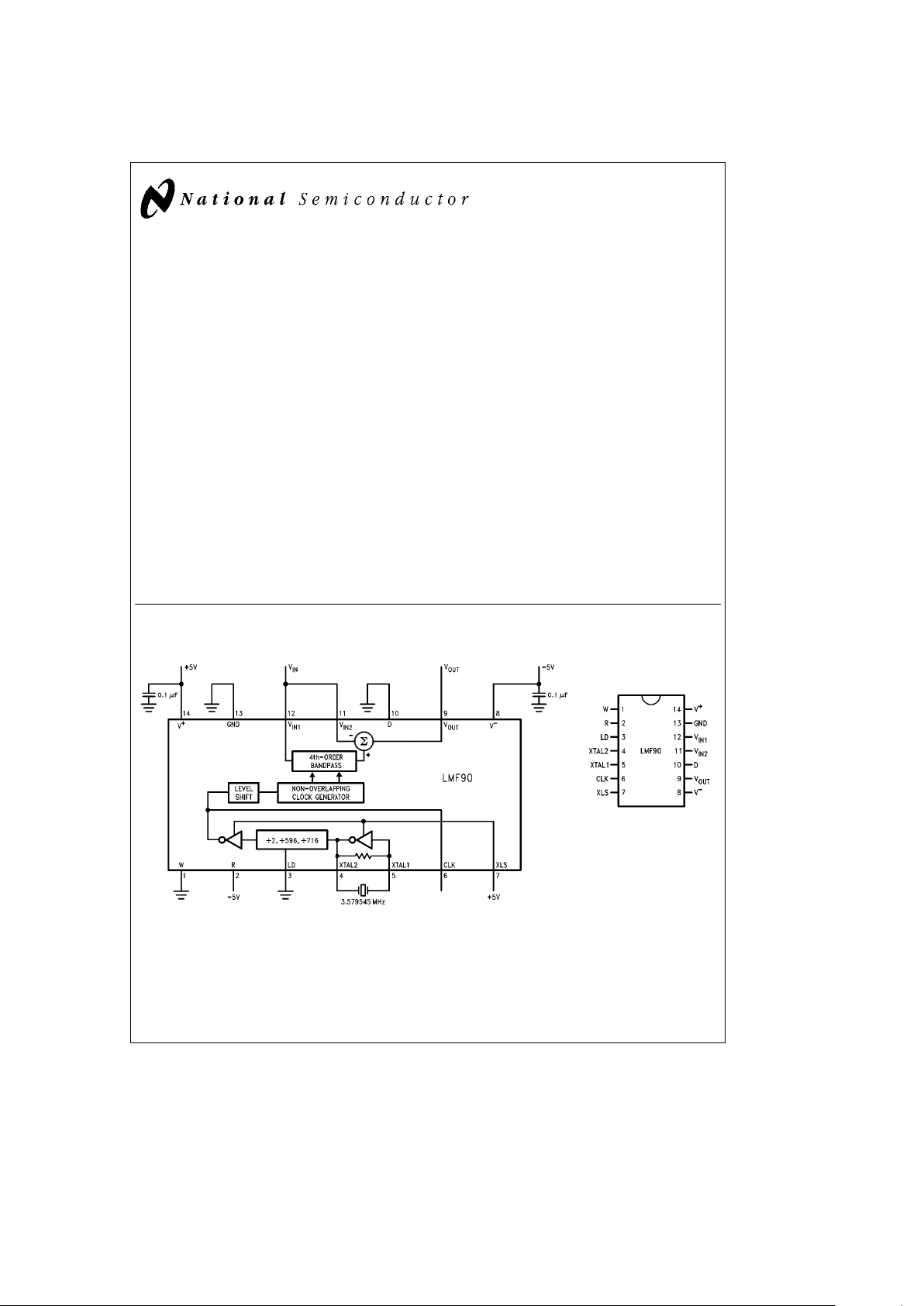
Typical Connection
60 Hz Notch Filter
TL/H/10354– 1
Connection
Diagram
Dual-In-Line and Small
Outline Packages
TL/H/10354– 2
Top View
Order Number LMF90CCN,
LMF90CIWM,
LMF90CCWM, LMF90CIJ,
LMF90CCJ, LMF90CIN,
LMF90CMJ or
LMF90CMJ/883
See NS Package Number
J14A, M14B or N14A
C
1995 National Semiconductor Corporation RRD-B30M115/Printed in U. S. A.
Absolute Maximum Ratings (Notes1&3)
If Military/Aerospace specified devices are required, Soldering Information (Note 4)
please contact the National Semiconductor Sales N Package (Soldering, 10 sec.) 260
§
C
Office/Distributors for availability and specifications. J Package (Soldering, 10 sec.) 300
§
C
Supply Voltage (V
S
e
V
a
b
V
b
)
b
0.3V to
a
16V Storage Temperature Range
b
65
§
Cto
a
150
§
C
Voltage at any Input or Output V
b
b
0.3V to V
a
a
0.3V Junction Temperature 150
§
C
Input Current at any Pin (Note 10) 5 mA
Operating Ratings (Notes2&3)
Package Input Current (Note 10) 20 mA
Temperature Range T
MIN
s
T
A
s
T
MAX
Power Dissipation (Note 5) 500 mW
LMF90CCN, LMF90CCWM,
ESD Susceptability (Note 6)
LMF90CCJ 0
§
C
s
T
A
s
a
70
§
C
Pin 9 1800V
LMF90CIJ, LMF90CIWM, LMF90CIN
All Other Pins 2000V
b
40
§
C
s
T
A
s
a
85
§
C
LMF90CMJ, LMF90CMJ/883
b
55
§
C
s
T
A
s
a
125
§
C
Supply Voltage Range 4.0V to 15.0V
AC Electrical Characteristics The following specifications apply for V
a
ea
5V and V
b
eb
5V unless otherwise specified. Boldface limits apply for
T
A
e
T
MIN
to T
MAX
; all other limits T
A
e
T
J
e
25
§
C.
LMF90CCJ, LMF90CCN, LMF90CIJ, LMF90CIWM,
LMF90CCWM LMF90CIN, LMF90CMJ
Units
Symbol Parameter Conditions
Typ
Tested Design
Typ
Tested Design (Limit)
(Note 7)
Limit Limit
(Note 7)
Limit Limit
(Note 8) (Note 9) (Note 8) (Note 9)
f
O
Center Frequency 0.1 0.1 Hz (Min)
Range 30 30 30 kHz (Max)
f
CLK
Clock Frequency Pin 6 10 10 Hz (Min)
Range Pin 6 1.5 1.5 1.5 MHz (Max)
Pins 4 and 5 4.0 4.0 4.0 MHz (Max)
f
CLK
/f
O1
Clock-to-Center- W
e
D
e
V
b
,R
e
V
a
,
33.5
g
1% 33.5
g
1.5% 33.5
g
1.5% (Max)
Frequency Ratio f
CLK
e
167 kHz
f
CLK
/f
O2
W
e
D
e
R
e
GND,
50.25
g
1% 50.25
g
1.5% 50.25
g
1.5% (Max)
f
CLK
e
250 kHz
f
CLK
/f
O3
W
e
V
a
,D
e
GND, R
e
V
b
,
100.5
g
1% 100.5
g
1.5% 100.5
g
1.5% (Max)
f
CLK
e
500 kHz
H
ON
Passband Gain DC and 20 kHz, W
e
D
e
V
b
,R
e
V
a
,
0
g
0.2
g
0.2 0
g
0.2 dB (Max)
f
CLK
e
167 kHz
W
e
D
e
R
e
GND,
0
g
0.2
g
0.2 0
g
0.2 dB (Max)
f
CLK
e
250 kHz
W
e
V
a
,D
e
GND, R
e
V
b
,
0
g
0.2
g
0.2 0
g
0.2 dB (Max)
f
CLK
e
500 kHz
2
AC Electrical Characteristics The following specifications apply for V
a
ea
5V and V
b
eb
5V unless otherwise specified. Boldface limits apply for
T
A
e
T
MIN
to T
MAX
; all other limits T
A
e
T
J
e
25
§
C. (Continued)
LMF90CCJ, LMF90CCN, LMF90CIJ, LMF90CIWM,
LMF90CCWM LMF90CIN, LMF90CMJ
Units
Symbol Parameter Conditions
Typ
Tested Design
Typ
Tested Design (Limit)
(Note 7)
Limit Limit
(Note 7)
Limit Limit
(Note 8) (Note 9) (Note 8) (Note 9)
PBW Ratio of Passband W
e
D
e
V
b
,R
e
V
a
,
0.1275
g
0.0175 0.1275
g
0.0175 0.1275
g
0.0175 (Max)
Width to Center f
CLK
e
167 kHz
Frequency W
e
D
e
R
e
GND,
0.265
g
0.025 0.265
g
0.025 0.265
g
0.025 (Max)
f
CLK
e
250 kHz
W
e
V
a
,D
e
GND, R
e
V
b
,
0.550
g
0.05 0.550
g
0.05 0.550
g
0.05 (Max)
f
CLK
e
500 kHz
A
Min1
@
f
O1
Gain at W
e
D
e
V
b
,R
e
V
a
,
b
39
b
30
b
30
b
39
b
30 dB (Max)
Center Frequency f
CLK
e
167 kHz
A
Min2
@
f
O2
W
e
D
e
R
e
GND,
b
48
b
36.5
b
36.5
b
48
b
36.5 dB (Max)
f
CLK
e
250 kHz
A
Min3
@
f
O3
W
e
V
a
,D
e
GND, R
e
V
b
,
b
48
b
36.5
b
36.5
b
48
b
36.5 dB (Max)
f
CLK
e
500 kHz
Additional Center W
e
GND, D
e
V
b
,R
e
V
a
,
b
36
b
30
b
30
b
36
b
30 dB (Max)
Frequency Gain f
CLK
e
167 kHz
Tests at f
O1
W
e
V
a
,D
e
V
b
,R
e
V
a
,
b
36
b
30
b
30
b
36
b
30 dB (Max)
f
CLK
e
167 kHz
W
e
V
b
,D
e
GND, R
e
V
a
,
b
42
b
30
b
30
b
42
b
30 dB (Max)
f
CLK
e
167 kHz
W
e
D
e
GND, R
e
V
a
,
b
48
b
35
b
35
b
48
b
35 dB (Max)
f
CLK
e
167 kHz
W
e
V
a
,D
e
GND,R
e
V
a
,
b
48
b
35
b
35
b
48
b
35 dB (Max)
f
CLK
e
167 kHz
3
AC Electrical Characteristics The following specifications apply for V
a
ea
5V and V
b
eb
5V unless otherwise specified. Boldface limits apply for
T
A
e
T
MIN
to T
MAX
; all other limits T
A
e
T
J
e
25
§
C. (Continued)
LMF90CCJ, LMF90CCN, LMF90CIJ, LMF90CIWM,
LMF90CCWM LMF90CIN, LMF90CMJ
Units
Symbol Parameter Conditions
Typ
Tested Design
Typ
Tested Design (Limit)
(Note 7)
Limit Limit
(Note 7)
Limit Limit
(Note 8) (Note 9) (Note 8) (Note 9)
Additional Center W
e
V
b
,D
e
V
b
,R
e
GND,
b
36
b
30
b
30
b
36
b
30 dB (Max)
Frequency Gain f
CLK
e
250 kHz
Tests at f
O2
W
e
GND, D
e
V
b
,R
e
GND,
b
36
b
30
b
30
b
36
b
30 dB (Max)
f
CLK
e
250 kHz
W
e
V
a
,D
e
V
b
,R
e
GND,
b
36
b
30
b
30
b
36
b
30 dB (Max)
f
CLK
e
250 kHz
W
e
V
b
,D
e
R
e
GND,
b
42
b
30
b
30
b
42
b
30 dB (Max)
f
CLK
e
250 kHz
W
e
V
a
,D
e
R
e
GND,
b
48
b
35
b
35
b
48
b
35 dB (Max)
f
CLK
e
250 kHz
Additional Center W
e
D
e
R
e
V
b
,
b
36
b
30
b
30
b
36
b
30 dB (Max)
Frequency Gain f
CLK
e
500 kHz
Tests at f
O3
W
e
GND, D
e
V
b
,R
e
V
b
,
b
36
b
30
b
30
b
36
b
30 dB (Max)
f
CLK
e
500 kHz
W
e
V
a
,D
e
V
b
,R
e
V
b
,
b
36
b
30
b
30
b
36
b
30 dB (Max)
f
CLK
e
500 kHz
W
e
V
b
,D
e
GND, R
e
V
b
,
b
42
b
30
b
30
b
42
b
30 dB (Max)
f
CLK
e
500 kHz
W
e
D
e
GND, R
e
V
b
,
b
48
b
35
b
35
b
48
b
35 dB (Max)
f
CLK
e
500 kHz
A
3a
Gain at f
3
e
0.995 f
O1
W
e
D
e
V
b
,R
e
V
a
,
b
41
b
30
b
30
b
41
b
30 dB (Max)
A
4a
Gain at f
4
e
1.005 f
O1
f
CLK
e
167 kHz
b
41
b
30
b
30
b
41
b
30 dB (Max)
A
3b
Gain at f
3
e
0.992 f
O2
W
e
D
e
R
e
GND, f
CLK
e
250 kHz
b
40
b
35
b
35
b
40
b
35 dB (Max)
A
4b
Gain at f
4
e
1.008 f
O2
b
40
b
35
b
35
b
40
b
35 dB (Max)
A
3c
Gain at f
3
e
0.982 f
O3
W
e
V
a
,D
e
GND, R
e
V
b
b
41
b
35
b
35
b
41
b
35 dB (Max)
A
4c
Gain at f
4
e
1.018 f
O3
f
CLK
e
500 kHz
b
41
b
35
b
35
b
41
b
35 dB (Max)
A
max1
Passband Ripple W
e
D
e
V
b
,R
e
V
a
,f
5
e
0.914 f
O1
0.25 0.9 0.9 0.25 0.9 dB (Max)
f
CLK
e
167 kHz 0.25 0 0 0.25 0 dB (Min)
f
6
e
1.094 f
O1
0.25 0.9 0.9 0.25 0.9 dB (Max)
0.25 0 0 0.25 0 dB (Min)
4
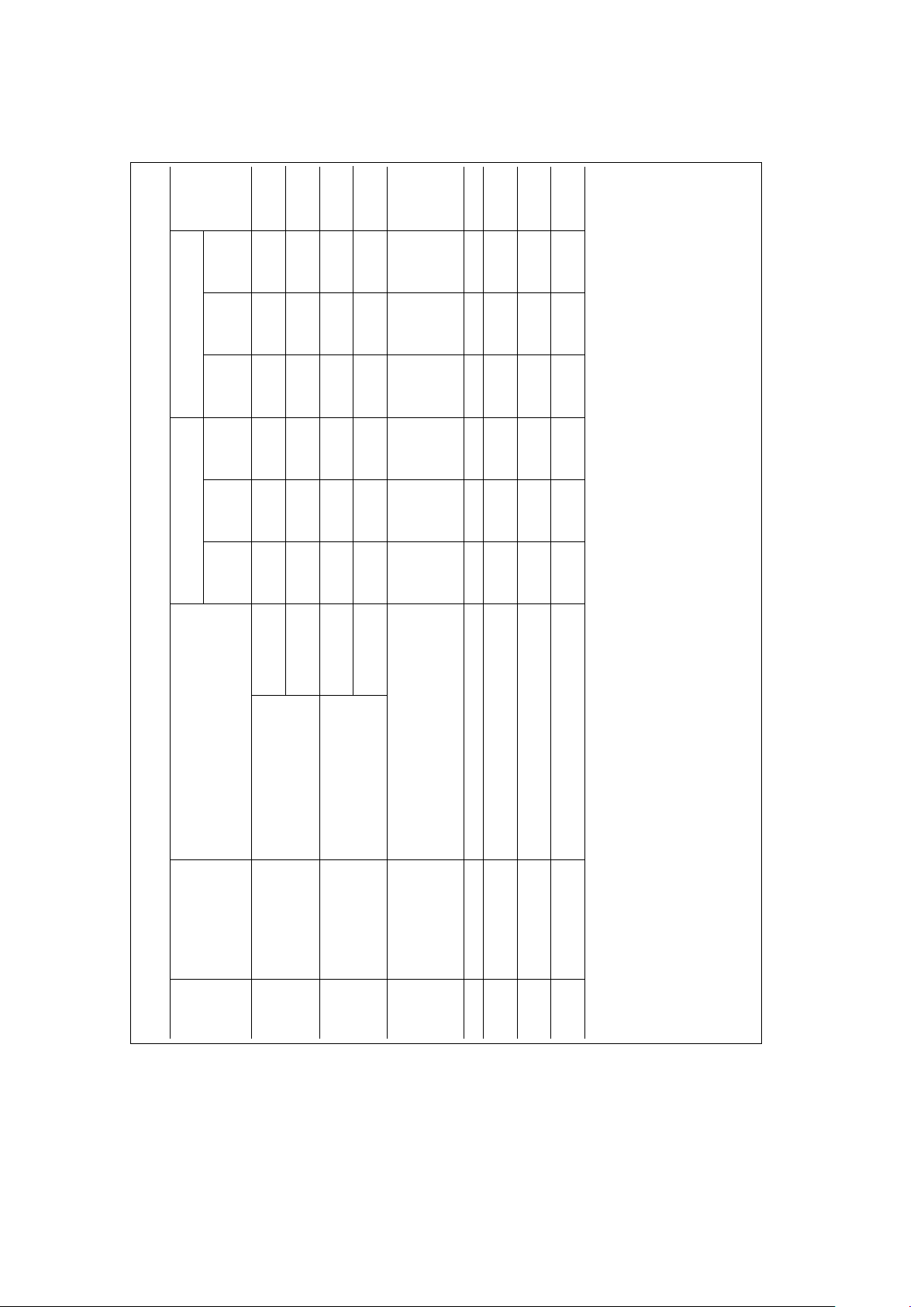
AC Electrical Characteristics The following specifications apply for V
a
ea
5V and V
b
eb
5V unless otherwise specified. Boldface limits apply for
T
A
e
T
MIN
to T
MAX
; all other limits T
A
e
T
J
e
25
§
C. (Continued)
LMF90CCJ, LMF90CCN, LMF90CIJ, LMF90CIWM,
LMF90CCWM LMF90CIN, LMF90CMJ
Units
Symbol Parameter Conditions
Typ
Tested Design
Typ
Tested Design (Limit)
(Note 7)
Limit Limit
(Note 7)
Limit Limit
(Note 8) (Note 9) (Note 8) (Note 9)
A
Max2
Passband Ripple W
e
D
e
R
e
GND, f
5
e
0.830 f
O2
0.25 0.9 0.9 0.26 0.9 dB (Max)
f
CLK
e
250 kHz 0.25 0 0 0.25 0 dB (Min)
f
6
e
1.205 f
O2
0.25 0.9 0.9 0.25 0.9 dB (Max)
0.25 0 0 0.25 0 dB (Min)
A
Max3
Passband Ripple W
e
V
a
,D
e
GND, R
e
V
b
f
5
e
0.700 f
O3
0.25 0.9 0.9 0.25 0.9 dB (Max)
f
CLK
e
500 kHz 0.25 0 0 0.25 0 dB (Min)
f
6
e
1.428 f
O3
0.25 0.9 0.9 0.25 0.9 dB (Max)
0.25 0 0 0.25 0 dB (Min)
E
n
Output Noise 20 kHz Bandwidth
W
e
D
e
V
b
,R
e
V
a
,f
CLK
e
167 kHz 670 670 mVrms
W
e
D
e
R
e
GND, f
CLK
e
250 kHz 370 370 mVrms
W
e
V
a
,D
e
GND, R
e
V
b
,
250 250 mVrms
f
CLK
e
500 kHz
Clock Feedthrough 50 50 mVp–p
GBW Output Buffer
1 1 MHz
Gain Bandwidth
SR Output Buffer
33V/ms
Slew Rate
C
L
Maximum Capacitive
200 200 pF
Load
5
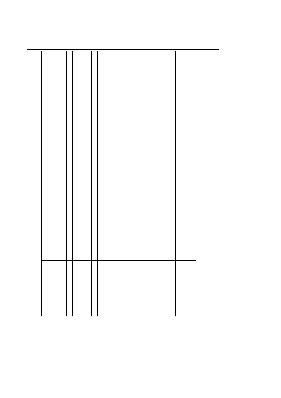
DC Electrical Characteristics The following specifications apply for V
a
ea
5V and V
b
eb
5V unless otherwise specified. Boldface Limits Apply for
T
A
e
T
MIN
to T
MAX
; all other limits T
A
e
T
J
e
25
§
C.
LMF90CCJ, LMF90CCN, LMF90CIJ, LMF90CIWM,
LMF90CCWM LMF90CIN, LMF90CMJ
Units
Symbol Parameter Conditions
Typ
Tested Design
Typ
Tested Design (Limit)
(Note 7)
Limit Limit
(Note 7)
Limit Limit
(Note 8) (Note 9) (Note 8) (Note 9)
I
S
Power Supply Current f
CLK
e
500 kHz, V
IN1
e
V
IN2
e
GND 2.35 5.0 5.0 2.35 5.0 mA (Max)
V
OS
Output Offset Voltage W
e
D
e
V
b
,R
e
V
a
,f
CLK
e
167 kHz
g
50
g
120
g
120
g
50
g
120 mV (Max)
W
e
D
e
R
e
GND, f
CLK
e
250 kHz
g
60
g
140
g
140
g
60
g
140 mV (Max)
W
e
V
a
,D
e
GND, R
e
V
b
,
g
80
g
170
g
170
g
80
g
170 mV (Max)
f
CLK
e
500 kHz
V
OUT
Output Voltage Swing R
L
e
5kX
a
4.2,
b
4.7
g
4.0
g
4.0
a
4.2,
b
4.7
g
4.0 V (Min)
V
I1
Logical ‘‘Low’’ Pins 1, 2, 3, 7, and 10
b
4.0
b
4.0
b
4.0 V (Max)
Input Voltage
V
I2
Logical ‘‘GND’’ Pins 1, 2, 3, 7, and 10
a
1.0
a
1.0
a
1.0 V (Max)
Input Voltage
b
1.0
b
1.0
b
1.0 V (Min)
V
I3
Logical ‘‘High’’ Pins 1, 2, 3, and 7
a
4.0
a
4.0
a
4.0 V (Min)
Input Voltage
I
IN
Input Current Pins 1, 2, 3, 7, and 10
g
10
g
10
g
10 mA (Max)
V
IL
Logical ‘‘0’’ Input Pin 5, XLS
e
V
a
b
4.0
b
4.0
b
4.0 V (Max)
Voltage, Pins 5 and 6 or Pin 6, XLS
e
GND
V
IH
Logical ‘‘1’’ Input
a
4.0
a
4.0
a
4.0 V(Min)
Voltage, Pins 5 and 6
V
IL
Logical ‘‘0’’ Input V
a
b
V
b
e
10V, XLS
e
V
b
or
a
0.8
a
0.8
a
0.8 V (Max)
Voltage, Pin 6 V
a
ea
5V, V
b
e
0V, XLS
ea
2.5V
V
IH
Logical ‘‘1’’ Input
a
2.0
a
2.0
a
2.0 V (Min)
Voltage, Pin 6
V
OL
Logical ‘‘0’’ Output XLS
e
V
a
,
l
I
OUT
l
e
4mA
b
4.0
b
4.0
b
4.0 V (Max)
Voltage, Pin 6
V
OH
Logical ‘‘1’’ Output
a
4.0
a
4.0
a
4.0 V (Min)
Voltage, Pin 6
6

DC Electrical Characteristics (Continued)
Note 1: Absolute Maximum Ratings indicate limits beyond which damage to the device may occur.
Note 2: Operating Ratings indicate conditions for which the device is intended to be functional. These ratings do not guarantee specific performance limits,
however. For guaranteed specifications and test conditions, see the Electrical Characteristics. The guaranteed specifications apply only for the test conditions
listed. Some performance characteristics may degrade when the device is not operated under the listed test conditions.
Note 3: All voltages are measured with respect to GND unless otherwise specified.
Note 4: See AN450 ‘‘Surface Mounting Methods and Their Effect on Product Reliability’’ or the section titled ‘‘Surface Mount’’ found in any current Linear Data
Book for other methods of soldering surface mount devices.
Note 5: The maximum power dissipation must be derated at elevated temperatures and is dictated by T
JMAX
, HJAand the ambient temperature, TA. The maximum
allowable power dissipation at any temperature is P
D
e
(T
JMAX
b
TA)/HJAor the number given in the Absolute Maximum Ratings, whichever is lower. For this
device, T
JMAX
e
150§C, and the typical thermal resistance (HJA) when board mounted is 61§C/W for the LMF90CCN and CIN, 134§C/W for the LMF90CCWM and
CWIM and 59
§
C/W for the LMF90CCJ, CIJ and CMJ.
Note 6: Human body model, 100 pF discharged through a 1.5 kX resistor.
Note 7: Typicals are at T
J
e
25§C and represent the most likely parametric norm.
Note 8: Tested Limits are guaranteed and 100% tested.
Note 9: Design Limits are guaranteed, but not 100% tested.
Note 10: When the input voltage (V
IN
) at any pin exceeds the power supplies (V
IN
k
Vbor V
IN
l
Va), the current at that pin should be limited to 5 mA. The 20 mA
maximum package input current rating limits the number of pins that can safely exceed the power supplies with an input current of 5 mA to four.
7
 Loading...