

NSC LMF60CIN-100 Datasheet
LMF60 High Performance
6th-Order Switched Capacitor
Butterworth Lowpass Filter
LMF60 High Performance 6th-Order Switched Capacitor Butterworth Lowpass Filter
May 1996
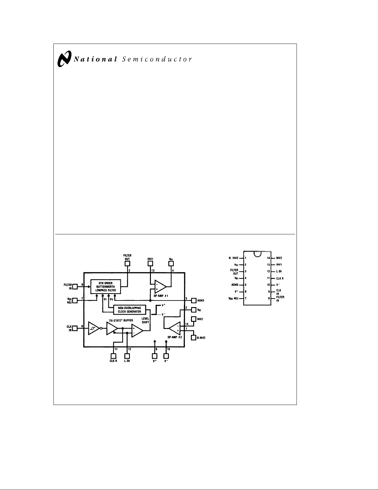
General Description
The LMF60 is a high performance, precision, 6th-order Butterworth lowpass active filter. It is fabricated using National’s LMCMOS process, an improved silicon-gate CMOS process specifically designed for analog products. Switchedcapacitor techniques eliminate external component requirements and allow a clock-tunable cutoff frequency. The ratio
of the clock frequency to the low-pass cutoff frequency is
internally set to 50:1 (LMF60-50) or 100:1 (LMF60-100). A
Schmitt trigger clock input stage allows two clocking options, either self-clocking (via an external resistor and capacitor) for stand-alone applications, or for tighter cutoff frequency control, a TTL or CMOS logic compatible clock can
be directly applied. The maximally flat passband frequency
response together with a DC gain of 1V/V allows cascading
LMF60 sections for higher-order filtering. In addition to the
filter, two independent CMOS op amps are included on the
die and are useful for any general signal conditioning applications. The LMF60 is pin- and functionally-compatible with
the MF6, but provides improved performance.
Block and Connection Diagrams
Features
Y
Cutoff frequency range of 0.1 Hz to 30 kHz
Y
Cutoff frequency accuracy ofg1.0%, maximum
Y
Low offset voltageg100 mV, maximum,g5V supply
Y
Low clock feedthrough of 10 mV
Y
Dynamic range of 88 dB, typical
Y
Two uncommitted op amps available
Y
No external components required
Y
14-pin DIP or 14-pin wide-body S.O. package
Y
Single/Dual Supply Operation:
a
4V toa14V (g2V tog7V)
Y
Cutoff frequency set by external or internal clock
Y
Pin-compatible with the MF6
p–p
, typical
Applications
Y
Communication systems
Y
Audio filtering
Y
Anti-alias filtering
Y
Data acquisition noise filtering
Y
Instrumentation
Y
High-order tracking filters
All Packages
Order Number LMF60CMJ-50,
See NS Package Number J14A
TL/H/9294– 1
Order Number LMF60CIWM-50
See NS Package Number M14B
Order Number LMF60CIN-50
See NS Package Number N14A
TRI-STATEÉis a registered trademark of National Semiconductor Corporation.
C
1996 National Semiconductor Corporation RRD-B30M56/Printed in U. S. A.
TL/H/9294
Top View
TL/H/9294– 2
(5962-9096 701MCA or
LMF60CMJ50/883),
LMF60CMJ-100, or
(5962-9096 702MCA
or LMF60CMJ100/883)
or LMF60CIWM-100
or LMF60CIN-100
Absolute Maximum Ratings (Note 1)
If Military/Aerospace specified devices are required,
please contact the National Semiconductor Sales
Office/Distributors for availability and specifications.
Supply Voltage (V
Voltage at Any Pin V
Input Current at Any Pin (Note 3) 5 mA
Package Input Current (Note 3) 20 mA
Power Dissipation (Note 4) 500 mW
Storage Temperature
ESD Susceptibility (Note 5) 2000V
CLK IN Pin 1700V
a
b
Vb) (Note 2) 15V
b
65§Ctoa150§C
a
a
0.2V
b
b
V
0.2V
Soldering Information:
N Package: 10 sec. 260§C
#
J Package: 10 sec. 300§C
#
SO Package: Vapor Phase (60 sec.) 215§C
#
Infrared (15 sec.) (Note 6) 220
Operating Ratings (Note 1)
s
Temperature Range T
LMF60CIN-50, LMF60CIN-100
LMF60CIJ-50, LMF60CIJ-100,
LMF60CIWM-50,
LMF60CIWM-100
b
40§CsT
LMF60CMJ-50, LMF60CMJ-100,
LMF60CMJ50/883,
LMF60CMJ100/883
Supply Voltage (V
a
b
Vb) 4Vto14V
b
55§CsT
Min
s
T
A
s
a
A
s
a
125§C
A
T
Max
85§C
C
§
Filter Electrical Characteristics
The following specifications apply for f
e
T
to T
MIN
; all other limits T
MAX
e
500 kHz (Note 7) unless otherwise specified. Boldface limits apply for T
CLK
e
e
T
A
25§C.
J
Symbol Parameter Conditions
a
V
f
CLK
I
S
H
o
f
CLK/fC
ea
b
eb
5V, V
5V
Clock Frequency Range 5 Hz (Min)
(Note 16) 1.5 MHz (Max)
Total Supply Current 7.0 / 12.0 mA (Max)
Clock Feedthrough V
DC Gain R
e
0V Filter 10 mVp-p
IN
Source
Opamp 5 mVp-p
s
2kX 0.10 / 0.10 dB (Max)
Clock to LMF60-50 49.00g0.8% /49.00g1.0% (Max)
Cutoff
Frequency LMF60-100 98.10
Ratio (Note 10)
Temperature Coefficient
of f
CLK/fC
A
V
V
I
MIN
OS
OUT
SC
Stopband Attenuation At 2cf
C
DC Offset LMF60-50
Voltage LMF60-100
Output Voltage
Swing (Note 2)
Output Short Circuit Source 90 mA
Current (Note 11) Sink 2.2 mA
Dynamic Range
(Note 12)
Additional
Magnitude
Response
Test Points
(Note 13)
LMF60-50
LMF60-100
e
f
12 kHz
IN
e
f
9 kHz
IN
e
f
6 kHz
IN
e
4.5 kHz
f
IN
e
A
Typical Limits Units
(Note 8) (Note 9) (Limits)
b
0.26 /b0.30 dB (Min)
g
0.8% /98.10g1.0% (Max)
4 ppm/
36 dB (Min)
g
100 mV (Max)
g
150 mV (Max)
a
3.9 /
b
4.2 /
a
3.7 V (Min)
b
4.0 V (Max)
88 dB
b
9.45g0.46 /b9.45g0.50 dB
b
0.87g0.16 /b0.87g0.20 dB
b
9.30g0.46 /b9.30g0.50 dB
b
0.87g0.16 /b0.87g0.20 dB
T
J
C
§
http://www.national.com 2
Filter Electrical Characteristics (Continued)
The following specifications apply for f
e
T
to T
MIN
; all other limits T
MAX
e
250 kHz (Note 7) unless otherwise specified. Boldface limits apply for T
CLK
e
e
T
A
25§C.
J
Symbol Parameter Conditions
a
V
f
CLK
I
S
H
o
f
CLK/fC
ea
b
2.5V, V
eb
2.5V
Clock Frequency Range 5 Hz (Min)
(Note 16) 750 kHz (Max)
Total Supply Current 5.0 / 6.5 mA (Max)
Clock Feedthrough V
(Peak to Peak) Opamp 3 mV
DC Gain (with f
s
R
Clock to
Cutoff
Source
2kX)
LMF60-50
Frequency
Ratio
(Note 10)
LMF60-100
e
0V Filter 6 mV
IN
e
250 kHz 0.10 / 0.10 dB (Max)
CLK
e
f
500 kHz
CLK
e
f
250 kHz 49.00g0.8% /49.00g1.0% (Max)
CLK
e
f
500 kHz 49.00g0.6%
CLK
e
f
250 kHz 98.10g0.8% /98.10g1.0% (Max)
CLK
e
500 kHz 98.10g0.6%
f
CLK
Temperature Coefficient
of f
CLK/fC
A
V
V
I
MIN
OS
OUT
SC
Stopband Attenuation At 2cf
C
DC Offset LMF60-50
Voltage LMF60-100
Output Voltage R
Swing (Note 2)
e
5kX
L
Output Short Circuit Source 42 mA
Current (Note 11) Sink 0.9 mA
Dynamic Range
(Note 12)
Additional
Magnitude
Response
Test Points
(Note 13)
LMF60-50
LMF60-100
f
f
f
f
IN
IN
IN
IN
e
6 kHz
e
4.5 kHz
e
3 kHz
e
2.25 kHz
e
T
A
Typical Limits Units
(Note 8) (Note 9) (Limits)
b
0.26 /b0.30 dB (Min)
b
0.08 dB
4 ppm/
36 dB (Min)
g
60 mV (Max)
g
90 mV (Max)
a
1.4 /
b
2.0 /
a
1.2 V (Min)
b
1.8 V (Max)
81 dB
b
9.45g0.46 /b9.45g0.50 dB
b
0.87g0.16 /b0.87g0.20 dB
b
9.30g0.46 /b9.30g0.50 dB
b
0.87g0.16 /b0.87g0.20 dB
J
C
§
http://www.national.com3
Op Amp Electrical Characteristics
Boldface limits apply for T
Symbol Parameter Conditions
a
ea
V
V
OS
I
B
CMRR Common Mode Rejection Test Input Range
V
O
I
SC
b
eb
5V, V
Input Offset Voltage
Input Bias Current 10 pA
Ratio (Op Amp
Output Voltage Swing R
Output Short Circuit Source 90 mA
Current (Note 13) Sink 2.1 mA
5V
A
e
Ý
2 Only)
e
T
T
to T
J
MIN
; all other limits T
MAX
e
e
T
A
25§C.
J
Typical Limits Units
(Note 8) (Note 9) (Limits)
g
20 mV (Max)
b
2.2V toa1.8V
e
5kX 3.8 / 3.6 V (Min)
L
e
55 dB
b
4.2 /b4.0 V (Max)
SR Slew Rate 4 V/ms
A
VOL
DC Open Loop Gain 80 dB (Min)
GBW Gain Bandwidth Product 2.0 MHz
a
ea
V
V
OS
I
B
CMRR Common Mode Rejection Test Input Range
V
O
I
SC
b
2.5V, V
eb
2.5V
Input Offset Voltage
g
20 mV (Max)
Input Bias Current 10 pA
Ý
Ratio (Op Amp
2 Only)
Output Voltage Swing R
b
0.9V toa0.5V
e
5kX 1.3 / 1.1 V (Min)
L
e
55 dB
b
1.8 /b1.6 V (Max)
Output Short Circuit Source 42 mA
Current (Note 13) Sink 0.9 mA
SR Slew Rate 3 V/ms
A
VOL
DC Open Loop Gain 74 dB (Min)
GBW Gain Bandwidth Product 2.0 MHz
Logic Input-Output Characteristics
The following specifications apply for V
e
e
T
T
to T
J
MIN
; all other limits T
MAX
b
e
0V (Note 15), L.She0V unless otherwise specified. Boldface limits apply for T
e
e
T
A
25§C.
J
Symbol Parameter Conditions
TTL CLOCK INPUT, CLK R PIN (NOTE 14)
a
a
ea
ea
5V, V
2.5V, V
V
IH
V
IL
V
IH
V
IL
TTL Input Logical ‘‘1’’ V
Voltage Logical ‘‘0’’ 0.8 V (Max)
CLK R Input Logical ‘‘1’’ V
Voltage Logical ‘‘0’’ 0.6 / 0.4 V (Max)
Maximum Leakage
Current at CLK R
http://www.national.com 4
Typical Limits Units
(Note 8) (Note 9) (Limits)
b
eb
5V 2.0 V (Min)
b
eb
2.5V 2.0 V (Min)
2.0 mA
A
Logic Input-Output Characteristics (Continued)
The following specifications apply for V
e
e
T
T
to T
J
MIN
Symbol Parameter Conditions
; all other limits T
MAX
b
e
0V (Note 15), L.She0V unless otherwise specified. Boldface limits apply for T
e
e
T
A
25§C.
J
Typical Limits Units
(Note 8) (Note 9) (Limits)
SCHMITT TRIGGER
a
V
a
T
Positive Going Input V
Threshold Voltage 8.8 / 8.9 V (Max)
e
10V 6.1 / 6.0 V (Min)
a
e
V
5V 3.0 / 2.9 V (Min)
4.3 / 4.4 V (Max)
a
V
b
T
Negative Going Input V
Threshold Voltage 3.8 / 3.9 V (Max)
e
10V 1.4 / 1.3 V (Min)
a
e
V
5V 0.7 / 0.6 V (Min)
1.9 / 2.0 V (Max)
b
V
V
a
b
T
T
Hysteresis V
a
e
10V 2.3 / 2.1 V (Min)
7.4 / 7.6 V (Max)
a
e
V
5V 1.1 / 0.9 V (Min)
3.6 / 3.8 V (Max)
a
V
OH
V
OL
I
SOURCE
I
SINK
Note 1: Absolute Maximum Ratings indicate limits beyond which damage to the device may occur. Operating Ratings indicate conditions for which the device is
functional. Specified Electrical Characteristics do not apply when operating the device outside its specified conditions.
Note 2: All voltages are measured with respect to AGND, unless otherwise specified.
Note 3: When the input voltage (V
to 5 mA or less. The 20 mA package input current limits the number of pins that can exceed the power supply boundaries with 5 mA to four.
Note 4: The Maximum power dissipation must be derated at elevated temperatures and is dictated by T
allowable power dissipation is PD
typical junction-to-ambient thermal resistance of the LMF60CCN when board mounted is 67
LMF60CIWM, i
Note 5: Human body model: 100 pF discharged through a 1.5 kX resistor.
Note 6: See AN450 ‘‘Surface Mounting Methods and Their Effect on Product Reliability’’ or the section titled ‘‘Surface Mount’’ found in any current Linear Databook
for other methods of soldering surface mount devices.
Note 7: The specifications given are for a clock frequency (f
deviate from the specified error band over the temperature range but the filter still maintains its amplitude characteristics. See application hints.
Note 8: Typicals are at 25
Note 9: Guaranteed to National’s Average Outgoing Quality Level (AOQL).
Note 10: The cutoff frequency of the filter is defined as the frequency where the magnitude response is 3.01 dB less than the DC gain of the filter.
Note 11: The short circuit source current is measured by forcing the output to its maximum positive swing and then shorting that output to the negative supply. The
short circuit sink current is measured by forcing the output being tested to its maximum negative voltage and then shorting that output to the positive supply. These
are worst case conditions.
Note 12: For
g
Note 13: The filter’s magnitude response is tested at the cutoff frequency, f
Note 14: The LMF60 is operated with symmetrical supplies and L.Sh is tied to GND.
Note 15: For simplicity all the logic levels (except for the TTL input logic levels) have been referenced to V
and
Note 16: The nominal ratio of the clock frequency to the low-pass cutoff frequency is internally set to 50-to-1 (LMF60-50) or 100-to-1 (LMF60-100).
g
2.5V supplies the dynamic range is referenced to 0.849 V
g
2.5V supplies.
Logical ‘‘1’’ Voltage V
eb
I
10 mA, Pin 11 V
O
Logical ‘‘0’’ Voltage V
eb
I
10 mA, Pin 11 V
O
Output Source CLK R to V
Current, Pin 11 V
Output Sink CLK R to V
Current, Pin 11 V
) at any pin exceeds the power supply rails (V
IN
e
b
(T
TA)/iJAor the number given in the absolute ratings, whichever is lower. For this device, T
J Max
e
78§C/W.
JA
) of 500 kHz ata5V and 250 kHz atg2.5V. Above this frequency, the cutoff frequency begins to
CLK
C and represent the most likely parametric norm.
§
5V supplies the dynamic range is referenced to 2.62 V
(1.2V peak), where the wideband noise over a 20 kHz bandwidth is typically 75 mV
rms
ea
10V 9.1 / 9.0 V (Min)
a
ea
5V 4.6 / 4.5 V (Min)
a
ea
10V 0.9 / 1.0 V (Max)
a
ea
5V 0.4 / 0.5 V (Max)
b
a
ea
10V 4.9 / 3.7 mA (Min)
a
ea
V
5V 1.6 / 1.2 mA (Min)
a
a
ea
10V 4.9 / 3.7 mA (Min)
a
ea
V
5V 1.6 / 1.2 mA (Min)
k
IN
(3.7V peak), where the wideband noise over a 20 kHz bandwidth is typically 100 mV. For
rms
,atf
C
IN
l
Vbor V
e
Va) the absolute value of current at that pin should be limited
IN
, iJA, and the ambient temperature TA. The maximum
J Max
C/W. For the LMF60CIJ this number decreases to 62§C/W. For the
§
2fC, and at these two additional frequencies.
b
e
0V. The logic levels will scale accordingly forg5V
J Max
e
125§C, and the
rms
.
A
http://www.national.com5
Typical Performance Characteristics
Deviation
f
CLK/fC
vs Power Supply Voltage
Deviation
f
CLK/fC
vs Power Supply Voltage
DC Gain Deviation
vs Power Supply Voltage
f
Deviation
CLK/fC
vs Temperature
f
Deviation
CLK/fC
vs Temperature
DC Gain Deviation
vs Temperature
f
Deviation
CLK/fC
vs Clock Frequency
f
Deviation
CLK/fC
vs Clock Frequency
DC Gain Deviation
vs Clock Frequency
http://www.national.com 6
TL/H/9294– 3
 Loading...