

NSC LMF100CIWMX, LMF100CIWM, LMF100CCN Datasheet
LMF100
High Performance Dual Switched Capacitor Filter
General Description
The LMF100 consists of two independent general purpose
high performance switched capacitor filters. With an external
clock and 2 to 4 resistors, various second-order and
first-order filtering functions can be realized by each filter
block. Each block has 3 outputs. One output can be configured to perform either an allpass, highpass, or notch function. The other two outputs perform bandpass and lowpass
functions. The center frequency of each filter stage is tuned
by usinganexternalclockor a combination of a clock and resistor ratio. Up to a 4th-order biquadratic function can be realized with a single LMF100. Higher order filters are implemented by simply cascading additional packages, and all the
classical filters (such as Butterworth, Bessel, Elliptic, and
Chebyshev) can be realized.
The LMF100 is fabricated on National Semiconductor’s high
performance analog silicon gate CMOS process,
LMCMOS
™
. This allows for the production of a very low offset, high frequency filter building block. The LMF100 is
pin-compatible with the industry standard MF10, but provides greatly improved performance.
Features
n Wide 4V to 15V power supply range
n Operation up to 100 kHz
n Low offset voltage: typically
(50:1 or 100:1 mode): Vos1
=
±
5mV
Vos2
=
±
15 mV
Vos3
=
±
15 mV
n Low crosstalk −60 dB
n Clock to center frequency ratio accuracy
±
0.2%typical
n f
0
x Q range up to 1.8 MHz
n Pin-compatible with MF10
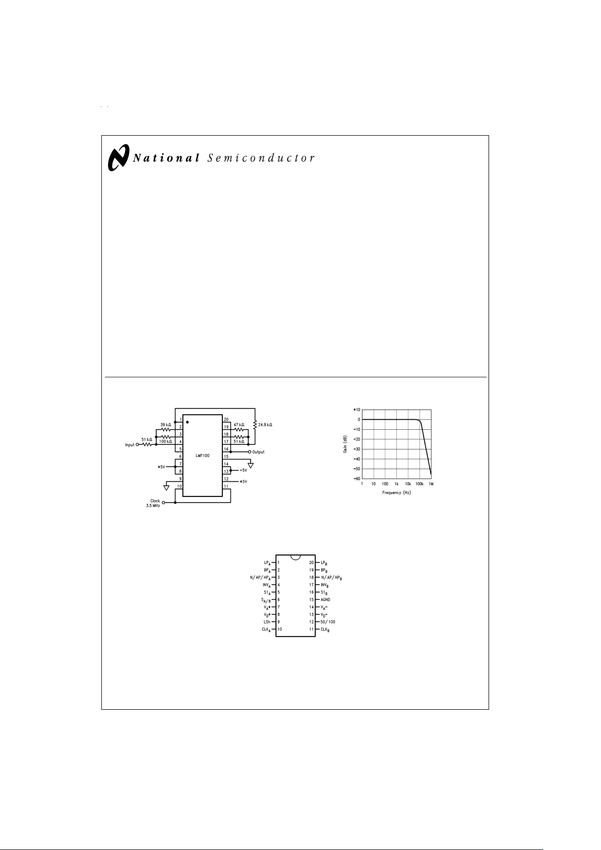
4th Order 100 kHz Butterworth Lowpass Filter
Connection Diagram
LMCMOS™is a trademark of National Semiconductor Corporation.
DS005645-2
DS005645-3
Surface Mount and Dual-In-Line Package
DS005645-18
Top View
Order Number
LMF100CCN or LMF100CIWM
See NS Package Number N20A or M20B
July 1999
LMF100 High Performance Dual Switched Capacitor Filter
© 1999 National Semiconductor Corporation DS005645 www.national.com
Absolute Maximum Ratings (Note 1)
If Military/Aerospace specified devices are required,
please contact the National Semiconductor Sales Office/
Distributors for availability and specifications.
(Note 14)
Supply Voltage (V
+−V−
) 16V
Voltage at Any Pin V
+
+ 0.3V
V
−
− 0.3V
Input Current at Any Pin (Note 2) 5 mA
Package Input Current (Note 2) 20 mA
Power Dissipation (Note 3) 500 mW
Storage Temperature 150˚C
ESD Susceptability (Note 11) 2000V
Soldering Information
N Package: 10 sec. 260˚C
J Package: 10 sec. 300˚C
SO Package:
Vapor Phase (60 sec.) 215˚C
Infrared (15 sec.) 220˚C
See AN-450 “Surface Mounting Methods and Their Effect
on Product Reliability” (Appendix D) for other methods of
soldering surface mount devices.
Operating Ratings (Note 1)
Temperature Range T
MIN
≤ TA≤ T
MAX
LMF100CCN 0˚C ≤ TA≤ +70˚C
LMF100CIWM −40˚C ≤ T
A
≤ +85˚C
Supply Voltage 4V ≤ V
+−V−
≤15V
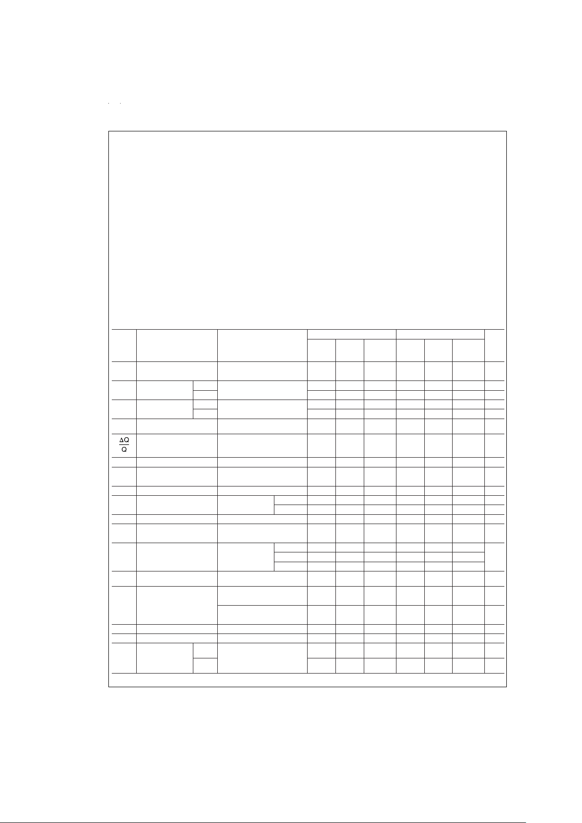
Electrical Characteristics
The following specifications apply for Mode 1, Q=10 (R
1
=
R
3
=
100k, R
2
=
10k), V
+
=
+5V and V
−
=
−5V unless otherwise
specified. Boldface limits apply for T
MIN
to T
MAX
; all other limits T
A
=
T
J
=
25˚C.
Symbol Parameter Conditions
LMF100CCN LMF100CIWM
Units
Typical
(Note 8)
Tested
Limit
(Note 9)
Design
Limit
(Note 10)
Typical
(Note 8)
Tested
Limit
(Note 9)
Design
Limit
(Note 10)
I
s
Maximum Supply Current f
CLK
=
250 kHz 9 13 13 9 13 mA
No Input Signal
f
0
Center Frequency MIN 0.1 0.1 Hz
Range MAX 100 100 kHz
f
CLK
Clock Frequency MIN 5.0 5.0 Hz
Range MAX 3.5 3.5 MHz
f
CLK/f0
Clock to Center Frequency
Ratio Deviation
V
Pin12
=
5V or 0V
f
CLK
=
1 MHz
±
0.2
±
0.8
±
0.8
±
0.2
±
0.8
%
Q Error (MAX) (Note 4) Q=10, Mode 1
V
Pin12
=
5V or 0V
f
CLK
=
1 MHz
±
0.5
±
5
±
6
±
0.5
±
6
%
H
OBP
Bandpass Gain at f
0
f
CLK
=
1 MHz 0
±
0.4
±
0.4 0
±
0.4 dB
H
OLP
DC Lowpass Gain R
1
=
R
2
=
10k 0
±
0.2
±
0.2 0
±
0.2 dB
f
CLK
=
250 kHz
V
OS1
DC Offset Voltage (Note 5) f
CLK
=
250 kHz
±
5.0
±
15
±
15
±
5.0
±
15 mV
V
OS2
DC Offset Voltage (Note 5) f
CLK
=
250 kHz S
A/B
=
V
+
±
30
±
80
±
80
±
30
±
80 mV
S
A/B
=
V
−
±
15
±
70
±
70
±
15
±
70 mV
V
OS3
DC Offset Voltage (Note 5) f
CLK
=
250 kHz
±
15
±
40
±
60
±
15
±
60 mV
Crosstalk (Note 6) A Side to B Side or
−60 −60 dB
B Side to A Side
Output Noise (Note 12) f
CLK
=
250 kHz N 40 40
20 kHz Bandwidth BP 320 320 µV
100:1 Mode LP 300 300
Clock Feedthrough
(Note 13)
f
CLK
=
250 kHz 100:1 Mode 6 6 mV
V
OUT
Minimum Output R
L
=
5k +4.0
±
3.8
±
3.7
+4.0
±
3.7 V
Voltage Swing (All Outputs) −4.7 −4.7
R
L
=
3.5k +3.9 +3.9
V
(All Outputs) −4.6 −4.6
GBW Op Amp Gain BW Product 5 5 MHz
SR Op Amp Slew Rate 20 20 V/µs
I
sc
Maximum Output
Short
Source (All Outputs) 12 12 mA
Circuit Current
(Note 7)
Sink 45 45 mA
www.national.com 2
Electrical Characteristics (Continued)
The following specifications apply for Mode 1, Q=10 (R
1
=
R
3
=
100k, R
2
=
10k), V
+
=
+5V and V
−
=
−5V unless otherwise
specified. Boldface limits apply for T
MIN
to T
MAX
; all other limits T
A
=
T
J
=
25˚C.
Symbol Parameter Conditions
LMF100CCN LMF100CIWM
Units
Typical
(Note 8)
Tested
Limit
(Note 9)
Design
Limit
(Note 10)
Typical
(Note 8)
Tested
Limit
(Note 9)
Design
Limit
(Note 10)
I
IN
Input Current on Pins: 4, 5, 10 10 µA
6, 9, 10, 11, 12, 16, 17
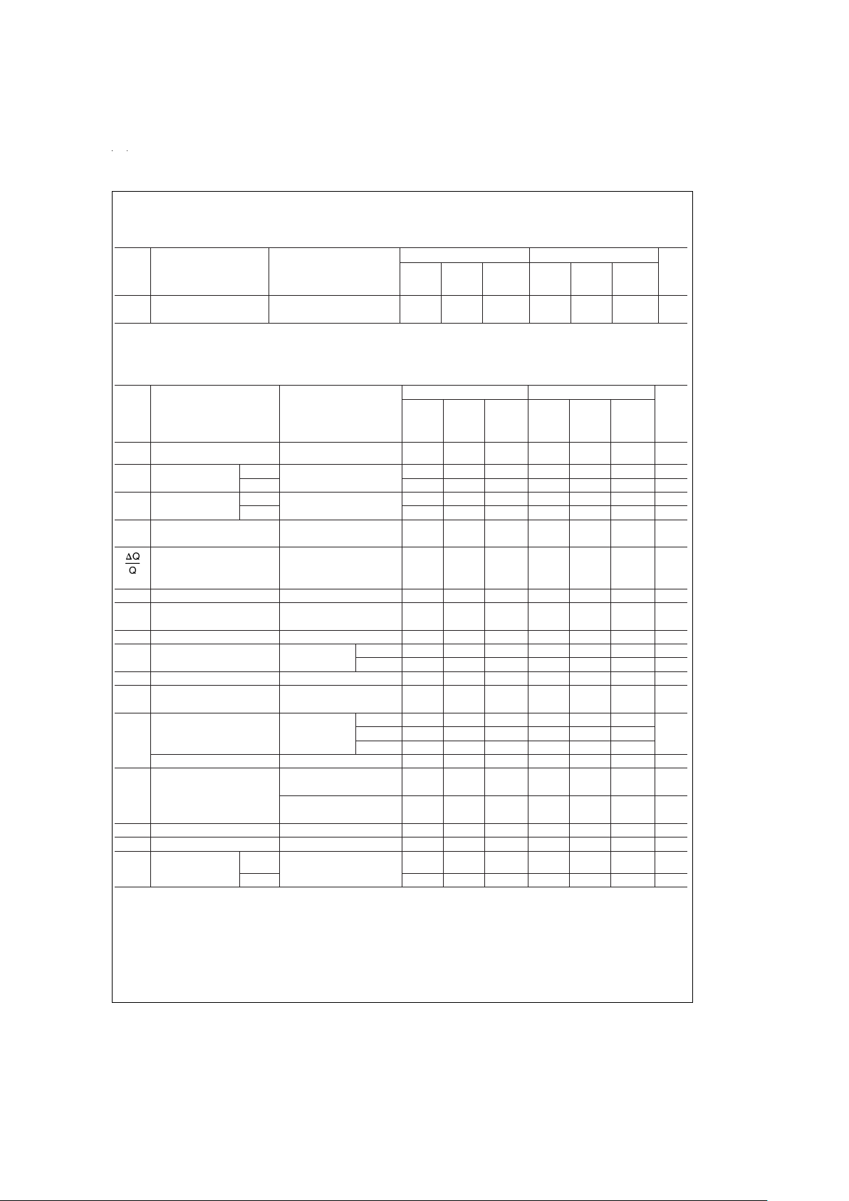
Electrical Characteristics
The following specifications apply for Mode 1, Q=10 (R
1
=
R
3
=
100k, R
2
=
10k), V
+
=
+2.50V and V
−
=
−2.50V unless oth-
erwise specified. Boldface limits apply for T
MIN
to T
MAX
; all other limits T
A
=
T
J
=
25˚C.
Symbol Parameter Conditions
LMF100CCN LMF100CIWM
Units
Typical
(Note 8)
Tested
Limit
(Note 9)
Design
Limit
(Note
10)
Typical
(Note 8)
Tested
Limit
(Note 9)
Design
Limit
(Note
10)
I
s
Maximum Supply
Current
f
CLK
=
250 kHz
No Input Signal
81212 8 12 mA
f
0
Center Frequency MIN 0.1 0.1 Hz
Range MAX 50 50 kHz
f
CLK
Clock Frequency MIN 5.0 5.0 Hz
Range MAX 1.5 1.5 MHz
f
CLK/f0
Clock to Center V
Pin12
=
2.5V or 0V
±
0.2
±
1
±
1
±
0.2
±
1
%
Frequency Ratio Deviation f
CLK
=
1 MHz
Q Error (MAX) Q=10, Mode 1
(Note 4) V
Pin12
=
5V or 0V
±
0.5
±
5
±
8
±
0.5
±
8
%
f
CLK
=
1 MHz
H
OBP
Bandpass Gain at f
0
f
CLK
=
1 MHz 0
±
0.4
±
0.5 0
±
0.5 dB
H
OLP
DC Lowpass Gain R
1
=
R
2
=
10k 0
±
0.2
±
0.2 0
±
0.2 dB
f
CLK
=
250 kHz
V
OS1
DC Offset Voltage (Note 5) f
CLK
=
250 kHz
±
5.0
±
15
±
15
±
5.0
±
15 mV
V
OS2
DC Offset Voltage (Note 5) f
CLK
=
250 kHz S
A/B
=
V
+
±
20
±
60
±
60
±
20
±
60 mV
S
A/B
=
V
−
±
10
±
50
±
60
±
10
±
60 mV
V
OS3
DC Offset Voltage (Note 5) f
CLK
=
250 kHz
±
10
±
25
±
30
±
10
±
30 mV
Crosstalk (Note 6) A Side to B Side or −65 −65 dB
B Side to A Side
Output Noise (Note 12) f
CLK
=
250 kHz N 25 25
20 kHz Bandwidth BP 250 250 µV
100:1 Mode LP 220 220
Clock Feedthrough (Note 13) f
CLK
=
250 kHz 100:1 Mode 2 2 mV
V
OUT
Minimum Output R
L
=
5k +1.6
±
1.5
±
1.4
+1.6
±
1.4 V
Voltage Swing (All Outputs) −2.2 −2.2
R
L
=
3.5k +1.5 +1.5 V
(All outputs) −2.1 −2.1
GBW Op Amp Gain BW Product 5 5 MHz
SR Op Amp Slew Rate 18 18 V/µs
I
sc
Maximum Output
Short Circuit
Source (All Outputs) 10 10 mA
Current (Note 7) Sink 20 20 mA
www.national.com3
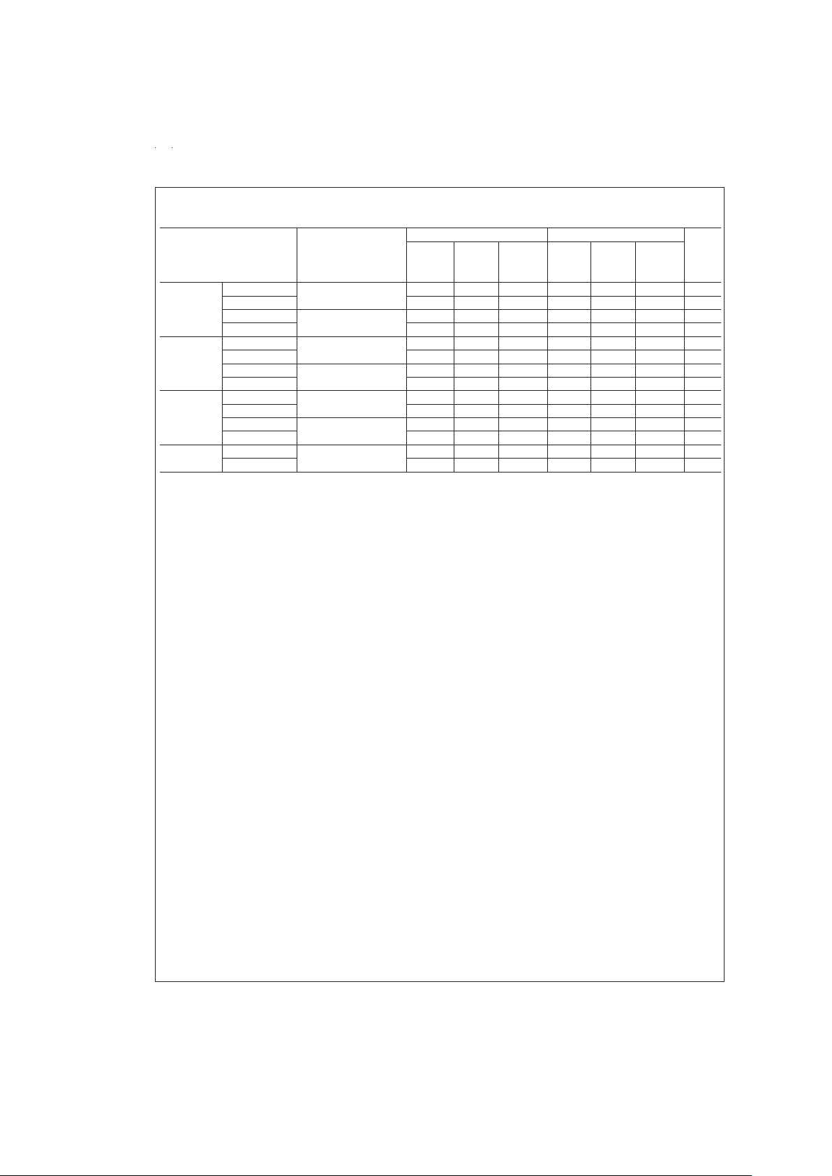
Logic Input Characteristics
Boldface limits apply for T
MIN
to T
MAX
; all other limits T
A
=
T
J
=
25˚C.
Parameter Conditions
LMF100CCN LMF100CIWM
Units
Typical Tested Design Typical Tested Design
(Note 8) Limit Limit (Note 8) Limit Limit
(Note 9) (Note 10) (Note 9) (Note 10)
CMOS Clock MIN Logical “1” V
+
=
+5V, V
−
=
−5V, +3.0 +3.0 +3.0 V
Input Voltage MAX Logical “0” V
LSh
=
0V −3.0 −3.0 −3.0 V
MIN Logical “1” V
+
=
+10V, V
−
=
0V, +8.0 +8.0 +8.0 V
MAX Logical “0” V
LSh
=
+5V +2.0 +2.0 +2.0 V
TTL Clock MIN Logical “1” V
+
=
+5V, V
−
=
−5V, +2.0 +2.0 +2.0 V
Input Voltage MAX Logical “0” V
LSh
=
0V +0.8 +0.8 +0.8 V
MIN Logical “1” V
+
=
+10V, V
−
=
0V, +2.0 +2.0 +2.0 V
MAX Logical “0” V
LSh
=
0V +0.8 +0.8 +0.8 V
CMOS Clock MIN Logical “1” V
+
=
+2.5V, V
−
=
−2.5V, +1.5 +1.5 +1.5 V
Input Voltage MAX Logical “0” V
LSh
=
0V −1.5 −1.5 −1.5 V
MIN Logical “1” V
+
=
+5V, V
−
=
0V, +4.0 +4.0 +4.0 V
MAX Logical “0” V
LSh
=
+2.5V +1.0 +1.0 +1.0 V
TTL Clock MIN Logical “1” V
+
=
+5V, V
−
=
0V, +2.0 +2.0 +2.0 V
Input Voltage MAX Logical “0” V
LSh
=
0V, V
D
+
=
0V +0.8 +0.8 +0.8 V
Note 1: Absolute Maximum Ratings indicate limits beyond which damage to the device may occur. Operating Ratings indicate conditions for which the device is intended to be functional. These ratings do not guarantee specific performance limits, however. For guaranteed specifications and test conditions, see the Electrical
Characteristics. The guaranteed specifications apply only for the test conditions listed. Some performance characteristics may degrade when the device is not operated under the listed test conditions.
Note 2: When the input voltage (V
IN
) at any pin exceeds the power supply rails (V
IN
<
V−or V
IN
>
V+) the absolute value of current at that pin should be limited
to 5 mA or less. The sum of the currents at all pins that are driven beyond the power supply voltages should not exceed 20 mA.
Note 3: The maximum power dissipation must be derated at elevated temperatures and is dictated by T
JMAX
, θJA, and the ambient temperature, TA. The maximum
allowable power dissipation at any temperature is P
D
=
(T
JMAX−TA
)/θJAor the number given in the Absolute Maximum Ratings, whichever is lower. For this device,
T
JMAX
=
125˚C, and the typical junction-to-ambient thermal resistance of the LMF100CIN when board mounted is 55˚C/W. For the LMF100CIWM this number is
66˚C/W.
Note 4: The accuracy of the Q value is afunction of the center frequency (f
0
). This is illustrated in the curves under the heading “TypicalPeformance Characteristics”.
Note 5: V
os1,Vos2
, and V
os3
refer to the internal offsets as discussed in the Applications Information section 3.4.
Note 6: Crosstalk between the internal filter sections is measured by applyinga1V
RMS
10 kHz signal to one bandpass filter section input and grounding the input
of the other bandpass filter section. The crosstalk is the ratio between the output of the grounded filter section and the 1 V
RMS
input signal of the other section.
Note 7: The short circuit source current is measured by forcing the output that is being tested to its maximum positive voltage swing and then shorting that output
to the negative supply. The short circuit sink current is measured by forcing the output that is being tested to its maximum negative voltage swing and then shorting
that output to the positive supply. These are the worst case conditions.
Note 8: Typicals are at 25˚C and represent most likely parametric norm.
Note 9: Tested limits are guaranteed to National’s AOQL (Average Outgoing Quality Level).
Note 10: Design limits are guaranteed to National’s AOQL (Average Outgoing Quality Level) but are not 100%tested.
Note 11: Human body model, 100 pF discharged through a 1.5 kΩ resistor.
Note 12: In 50:1 mode the output noise is 3 dB higher.
Note 13: In 50:1 mode the clock feedthrough is 6 dB higher.
Note 14: A military RETS specification is available upon request.
www.national.com 4
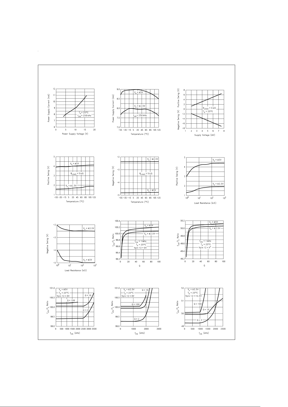
Typical Performance Characteristics
Power Supply Current vs
Power Supply Voltage
DS005645-40
Power Supply Current vs
Temperature
DS005645-41
Output Swing vs
Supply Voltage
DS005645-42
Positive Output Swing
vs Temperature
DS005645-43
Negative Output Swing
vs Temperature
DS005645-44
Positive Output Voltage
Swing vs Load Resistance
DS005645-45
Negative Output Voltage
Swing vs Load Resistance
DS005645-46
f
CLK/f0
Ratio vs Q
DS005645-47
f
CLK/f0
Ratio vs Q
DS005645-48
f
CLK/f0
Ratio vs f
CLK
DS005645-49
f
CLK/f0
Ratio vs f
CLK
DS005645-50
f
CLK/f0
Ratio vs f
CLK
DS005645-51
www.national.com5
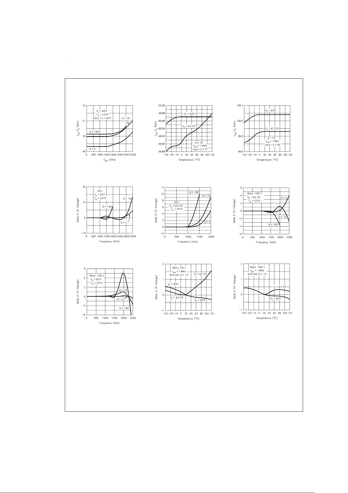
Typical Performance Characteristics (Continued)
f
CLK/f0
Ratio vs f
CLK
DS005645-52
f
CLK/f0
Ratio vs Temperature
DS005645-53
f
CLK/f0
Ratio vs Temperature
DS005645-54
Q Deviation vs Clock
Frequency
DS005645-55
Q Deviation vs Clock
Frequency
DS005645-56
Q Deviation vs Clock
Frequency
DS005645-57
Q Deviation vs Clock
Frequency
DS005645-58
Q Deviation vs Temperature
DS005645-59
Q Deviation vs Temperature
DS005645-60
www.national.com 6
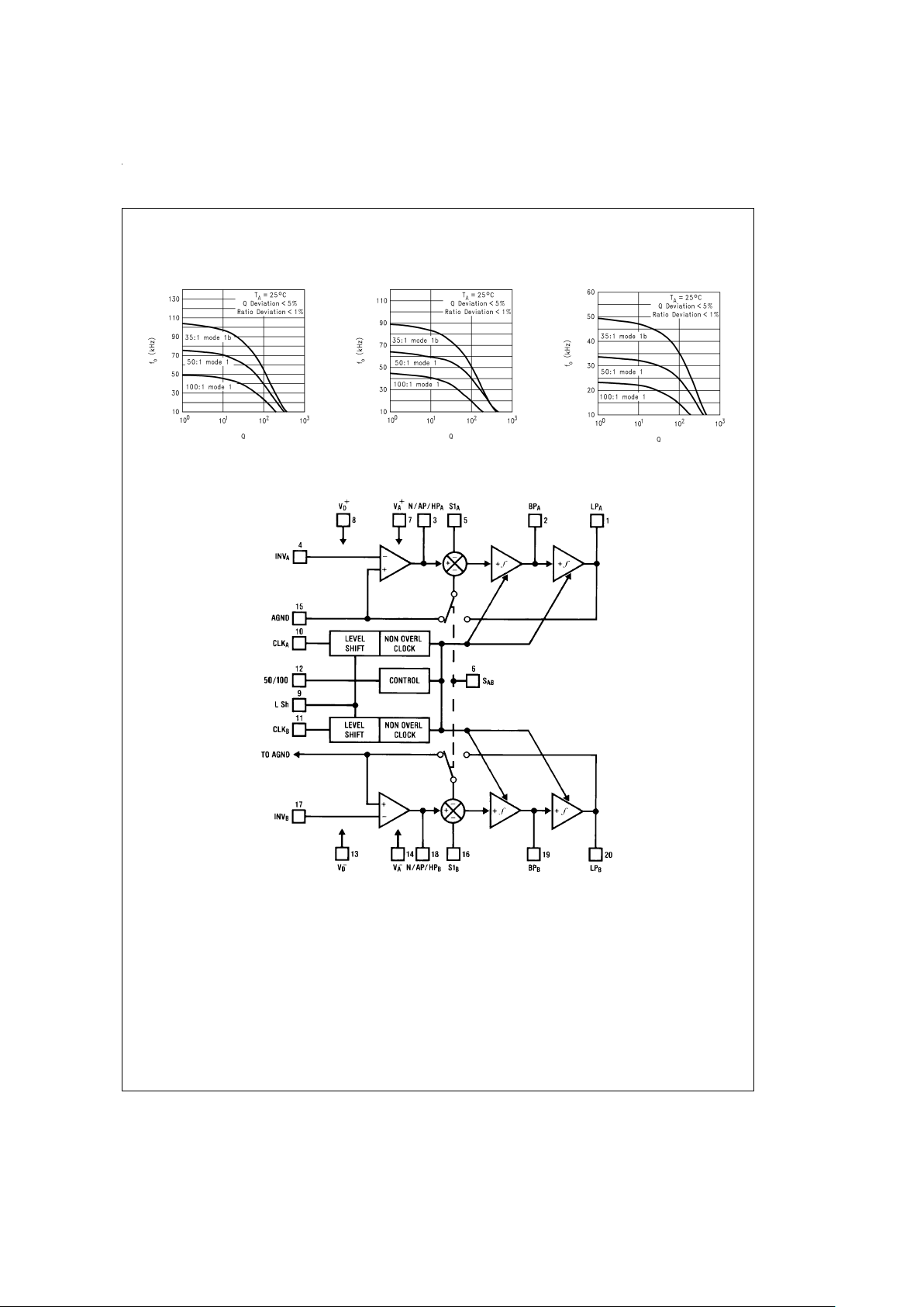
Typical Performance Characteristics (Continued)
LMF100 System Block Diagram
Maximum f0vsQat
V
s
=
±
7.5V
DS005645-61
Maximum f0vsQat
V
s
=
±
5.0V
DS005645-62
Maximum f0vsQat
V
s
=
±
2.5V
DS005645-63
DS005645-1
www.national.com7

Pin Descriptions
LP(1,20),
BP(2,19),
N/AP/HP(3,18)
The second order lowpass,
bandpass and
notch/allpass/highpass outputs.
These outputs can typically swing
to within 1V of each supply when
drivinga5kΩload. For optimum
performance, capacitive loading
on these outputs should be
minimized. For signal frequencies
above 15 kHz the capacitance
loading should be kept below
30 pF.
INV(4,17) The inverting input of the
summing opamp of each filter.
These are high impedance inputs.
The non-inverting input is
internally tied to AGND so the
opamp can be used only as an
inverting amplifier.
S1(5,16) S1 is a signal input pin used in
modes 1b, 4, and 5. The input
impedance is 1/f
CLK
x 1 pF. The
pin should be driven with a source
impedance of less than 1 kΩ.If
S1 is not driven with a signal it
should be tied to AGND
(mid-supply).
S
A/B
(6) This pin activates a switch that
connects one of the inputs of each
filter’s second summer either to
AGND (S
A/B
tied to V−)ortothe
lowpass (LP) output (S
A/B
tied to
V
+
). This offers the flexibility
needed for configuring the filter in
its various modes of operation.
V
A
+
(7) (Note 15) This is both the analog and digital
positive supply.
V
D
+
(8) (Note 15) This pin needs to be tied to V
+
except when the device is to
operate on a single 5V supply and
a TTL level clock is applied. For
5V, TTL operation, V
D
+
should be
tied to ground (0V).
V
A
−
(14), V
D
−
(13) Analog and digital negative
supplies. V
A
−
and V
D
−
should be
derived from the same source.
They have been brought out
separately so they can be
bypassed by separate capacitors,
if desired. They can also be tied
together externally and bypassed
with a single capacitor.
LSh(9) Level shift pin. This is used to
accommodate various clock levels
with dual or single supply
operation. With dual
±
5V supplies
and CMOS (
±
5V) or TTL (0V–5V)
clock levels, LSh should be tied to
system ground.
For 0V–10V single supply
operation the AGND pin should be
biased at +5V and the LSh pin
should be tied to the system
ground for TTL clock levels. LSh
should be biased at +5V for
±
5V
CMOS clock levels.
The LSh pin is tied to system
ground for
±
2.5V operation. For
single 5V operation the LSh and
V
D
+ pins are tied to system
ground for TTL clock levels.
CLK(10,11) Clock inputs for the two switched
capacitor filter sections. Unipolar
or bipolar clock levels may be
applied to the CLK inputs
according to the programming
voltage applied to the LSh pin.
The duty cycle of the clock should
be close to 50%, especially when
clock frequencies above 200 kHz
are used. This allows the
maximum time for the internal
opamps to settle, which yields
optimum filter performance.
50/100(12)
(Note 15)
By tying this pin to V
+
a 50:1 clock
to filter center frequency ratio is
obtained. Tying this pin at
mid-supply (i.e., system ground
with dual supplies) or to V
−
allows
the filter to operate at a 100:1
clock to center frequency ratio.
AGND(15) This is the analog ground pin.
This pin should be connected to
the system ground for dual supply
operation or biased to mid-supply
for single supply operation. For a
further discussion of mid-supply
biasing techniques see the
Applications Information (Section
3.2). For optimum filter
performance a “clean” ground
must be provided.
Note 15: This device is pin-for-pin compatible with the MF10 except for the
following changes:
1. Unlike the MF10, the LMF100 has a single positive supply pin (V
A
+).
2. On the LMF100 V
D
+
is a control pin and is not the digital positive supply as
on the MF10.
3. Unlike the MF10, the LMF100 does not support the current limiting mode.
When the 50/100 pin is tied to V
−
the LMF100 will remain in the 100:1 mode.
www.national.com 8
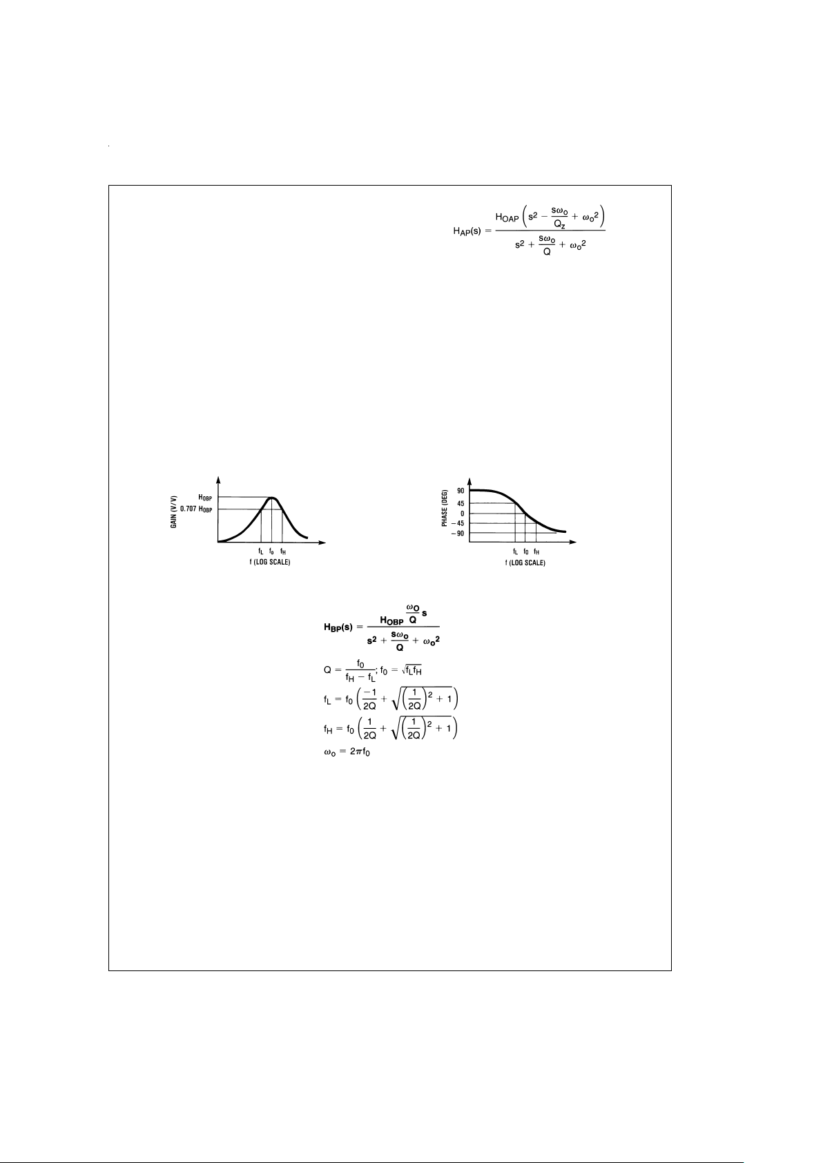
1.0 Definitions of Terms
f
CLK
: the frequency of the external clock signal applied to pin
10 or 11.
f
0
: center frequency of the second order function complex
pole pair. f
0
is measured at the bandpass outputs of the
LMF100, and is the frequency of maximum bandpass gain.
(
Figure 1
).
f
notch
: the frequency of minimum (ideally zero) gain at the
notch outputs.
f
z
: the center frequency of the second order complex zero
pair, if any. If f
z
is different from f0and if Qzis high, it can be
observed as the frequency of a notch at the allpass output.
(
Figure 13
).
Q: “quality factor” of the 2nd order filter.Q is measured at the
bandpass outputs of the LMF100 and is equal to f
0
divided
by the −3 dB bandwidth of the 2nd order bandpass filter (
Fig-
ure 1
). The value of Q determines the shape of the 2nd order
filter responses as shown in
Figure 6
.
Q
z
: the quality factor of the second order complex zero pair,
if any. Q
Z
is related to the allpass characteristic, which is
written:
where Q
Z
=
Q for an all-pass response.
H
OBP
: the gain (in V/V) of the bandpass output at f=f0.
H
OLP
: the gain (in V/V) of the lowpass output as f→0Hz
(
Figure 2
).
H
OHP
: the gain (in V/V) of the highpass output as f→f
CLK
/2
(
Figure 3
).
H
ON
: the gain (in V/V) of the notch output as f→0 Hz and as
f→f
CLK
/2, when the notch filter has equal gain above and
below the center frequency (
Figure 4
). When the
low-frequency gain differs from the high-frequency gain, as
in modes 2 and 3a (
Figure 10
and
Figure 12
), the two quan-
tities below are used in place of H
ON
.
H
ON1
: the gain (in V/V) of the notch output as f→0 Hz.
H
ON2
: the gain (in V/V) of the notch output as f→f
CLK
/2.
DS005645-19
(a)
DS005645-20
(b)
FIGURE 1. 2nd-Order Bandpass Response
www.national.com9
 Loading...