

January 16, 2008
LME49830
Mono High Fidelity 200 Volt MOSFET Power Amplifier Input
Stage with Mute
General Description
The LME49830 is a high fidelity audio power amplifier input
stage designed for demanding consumer and pro-audio applications. Amplifier output power may be scaled by changing
the supply voltage and number of output devices. The
LME49830 is capable of driving an output stage in excess of
300 W single-ended into an 8Ω load in the presence of 10%
high line headroom and 20% supply regulation.
The LME49830 includes internal thermal shut down circuitry
that activates when the LME49830 die temperature exceeds
150°C. The LME49830 has a mute function that mutes the
input drive signal and forces the amplifier output to a quiescent state.
The LME49830 has high drive current, 56mA typical, and high
output voltage swing for maximum flexibility in output stage
choice. With a bias voltage range up to 16V the LME49830
can be used to drive MOSFET output stages using a wide
selection of MOSFETs.
The LME49830 has a wide operating supply range of ±20V
to ±100V, which allows lower cost, unregulated power supplies to be used.
Key Specifications
■ Wide operating Voltage range ±20V to ±100V
■ Output Voltage Noise (BW =
30kHz) 44μV (typ)
■ PSRR (DC) 105dB (typ)
■ Slew Rate 39V/μs (typ)
■ THD+N (f = 1kHz) 0.0006% (typ)
Features
■
High output current and voltage for use with MOSFET
output stages
■
Very high voltage range: ±20V - ±100V
■
Scalable output power
■
Minimum external components
■
External compensation
■
Thermal shutdown of input stage
■
Mute control
Applications
■
AV receivers
■
Audiophile power amps
■
Pro Audio
■
High voltage industrial applications
Overture® is a registered trademark of National Semiconductor Corporation.
© 2008 National Semiconductor Corporation 300050 www.national.com
LME49830 Mono High Fidelity 200 Volt MOSFET Power Amplifier Input Stage with Mute
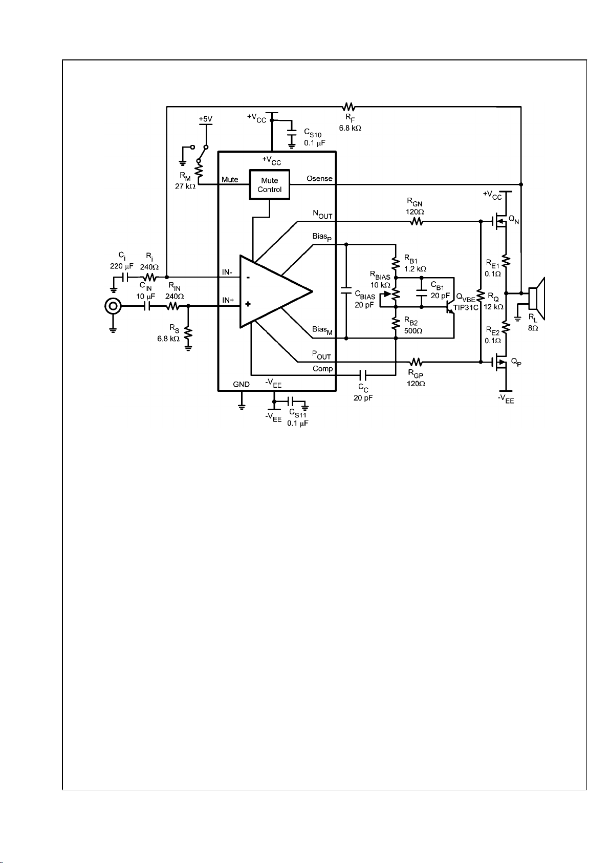
Typical Application
30005090
FIGURE 1. Typical Audio Amplifier Application Circuit
www.national.com 2
LME49830
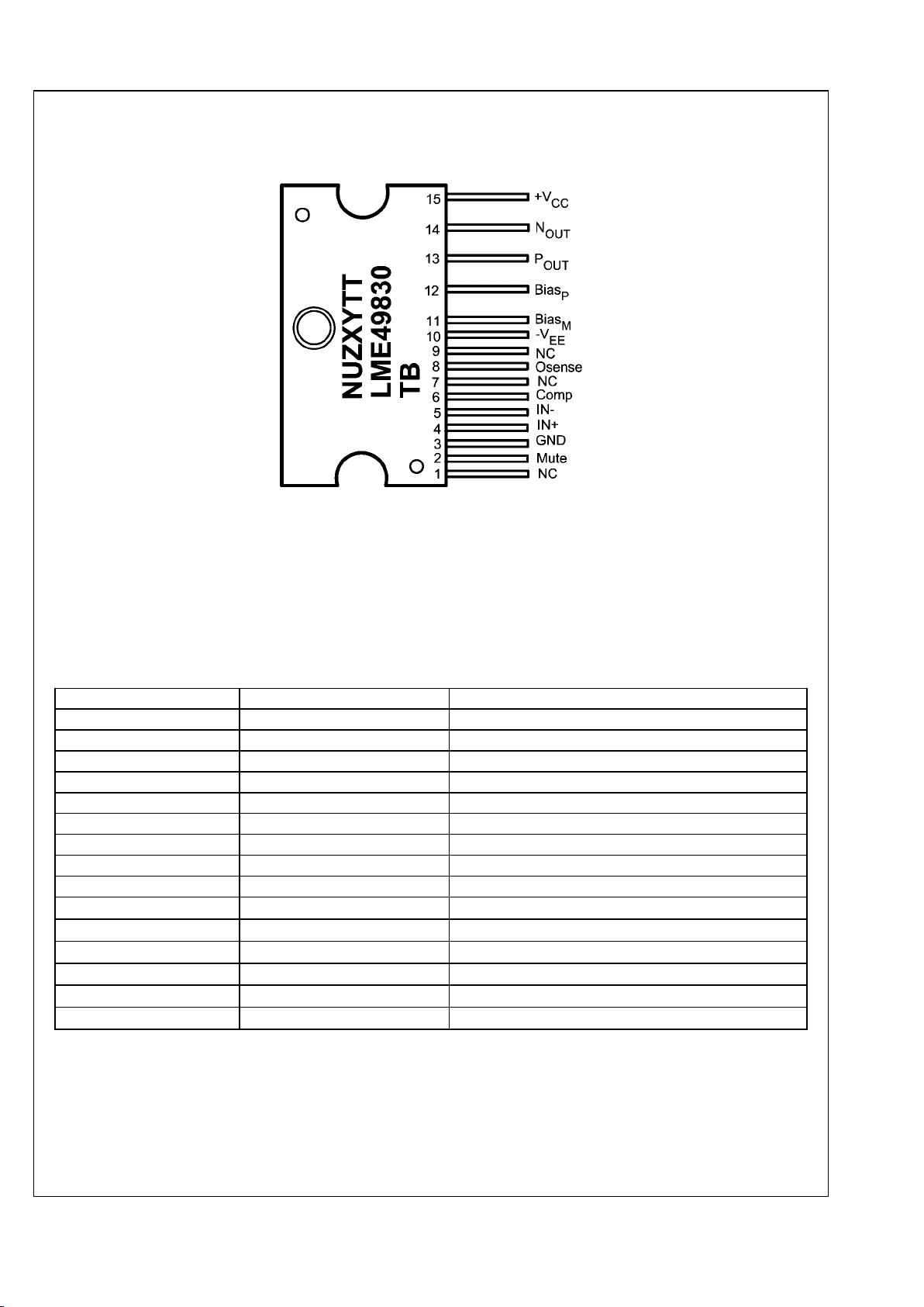
Connection Diagram
Plastic Package (Note 8)
30005049
Top View
Order Number LME49830TB
See NS Package Number TB15A
N = National logo
U = Fabrication plant code
Z = Assembly plant code
XY = 2 Digit date code
TT = Die traceability
TB = Package code
Pin Descriptions
Pin Pin Name Description
1 NC No Connection, Pin electrically isolated
2 Mute Mute Control
3 GND Device Ground
4 IN+ Non-inverting input
5 IN- Inverting input
6 Comp External Compensation Connection
7 NC No Connection, Pin electrically isolated
8 Osense Output Sense
9 NC No Connection, Pin electrically isolated
10 -V
EE
Negative Power Supply
11 Bias
M
Negative External Bias Control
12 Bias
P
Positive External Bias Control
13 P
OUT
P-channel MOSFET Output
14 N
OUT
N-channel MOSFET Output
15 +V
CC
Positive Power Supply
3 www.national.com
LME49830
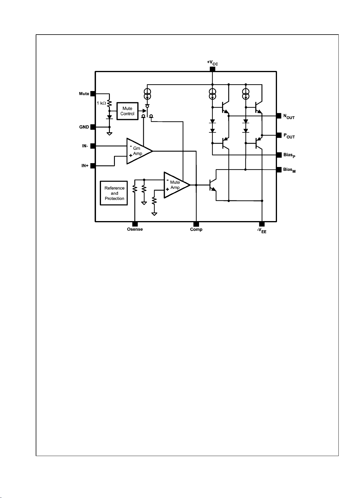
Block Diagram
30005091
FIGURE 2. LME49830 Simplified Block Diagram
www.national.com 4
LME49830
Absolute Maximum Ratings (Notes 1, 2)
If Military/Aerospace specified devices are required,
please contact the National Semiconductor Sales Office/
Distributors for availability and specifications.
Supply Voltage |V+| + |V-|
200V
Differential Input Voltage +/-6V
Common Mode Input Range 0.4 V
EE
to 0.4 V
CC
Power Dissipation (Note 3) 5.4W
ESD Rating (Note 4) 2.0kV
ESD Rating (Note 5) 200V
Junction Temperature (T
JMAX
)
150°C
Soldering Information
TB Package (10 seconds) 260°C
Storage Temperature -40°C to +150°C
Thermal Resistance
θ
JA
73°C/W
θ
JC
4°C/W
Operating Ratings (Notes 1, 2)
Temperature Range
T
MIN
≤ TA ≤ T
MAX
−40°C ≤ TA ≤ +85°C
Supply Voltage
±20V ≤ V
SUPPLY
≤ ±100V
Electrical Characteristics VCC = +100V, VEE = –100V (Notes 1, 2)
The following specifications apply for I
MUTE
= 150μA unless otherwise specified. Limits apply for TA = 25°C.
Symbol Parameter Conditions
LME49830
Units
(Limits)
Typical Limit
(Note 6) (Note 7)
I
CC
Total Positive Quiescent Power
Supply Current
VIN = 0V, VO = 0V, IO = 0A
19 24 mA (max)
I
EE
Total Negative Quiescent Power
Supply Current
VIN = 0V, VO = 0V, IO = 0A
–21 mA
THD+N
Total Harmonic Distortion +
Noise
No load, f = 1kHz, AV = 30dB
V
OUT
= 30V
RMS
, 30kHz BW
0.0006
%
V
BIAS
Bias Voltage 16 15 V (min)
A
V(CL)
Closed Loop Voltage Gain 26 dB (min)
A
V(OL)
Open Loop Gain
f = DC
V
IN
= 1mV
RMS
, f = 1kHz, CC = 10pF
112
88
82 dB (min)
V
OM
Output Voltage Swing THD = 0.05%, f = 20Hz to 20kHz 68 V
RMS
V
NOISE
Output Noise
RS = 10kΩ, AV = 30dB,
30kHz BW
A-weighted
44
28
μV (max)
μV (max)
I
OUT
Maximum Output Current Current from Output pins 56 47 mA (min)
I
MUTE
Current into Mute Pin To put part in “play” mode
130
μA (min)
SR Slew Rate
VIN = 1.2V
P-P
, AV = 30dB,
f = 10kHz square wave, C
LOAD
= 2,000pF
39
V/μs (min)
V
OS
Input Offset Voltage
VCM = 0V, IO = 0mA, I
MUTE
= 150μA
±0.9 ±3 mV (max)
VCM = 0V, IO = 0mA, I
MUTE
= 0μA
±0.4 ±4.2 mV (max)
I
B
Input Bias Current VCM = 0V, IO = 0mA
95 170 nA (max)
PSRR
AC
Power Supply Rejection Ratio
(AC)
RS = 1kΩ, f = 100Hz,V
RIPPLE
= 1V
RMS
,
Input Referred, AV = 30dB
104 dB
PSRR
DC
Power Supply Rejection Ratio
(DC)
RS = 1kΩ, Input Referred,
AV = 30dB
105 94 dB (min)
I
AB
Bias Control Current Shorted output, shorted bias control 2
1.6
2.5
mA (min)
mA (max)
5 www.national.com
LME49830
Note 1: “Absolute Maximum Ratings” indicate limits beyond which damage to the device may occur, including inoperability and degradation of device reliability
and/or performance. Functional operation of the device and/or non-degradation at the Absolute Maximum Ratings or other conditions beyond those indicated in
the Recommended Operating Conditions is not implied. The Recommended Operating Conditions indicate conditions at which the device is functional and the
device should not be operated beyond such conditions. All voltages are measured with respect to the ground pin, unless otherwise specified.
Note 2: The Electrical Characteristics tables list guaranteed specifications under the listed Recommended Operating Conditions except as otherwise modified
or specified by the Electrical Characteristics Conditions and/or Notes. Typical specifications are estimations only and are not guaranteed.
Note 3: The maximum power dissipation must be derated at elevated temperatures and is dictated by T
JMAX
, θJA, and the ambient temperature, TA. The maximum
allowable power dissipation is P
DMAX
= (T
JMAX
- TA) / θJA or the number given in Absolute Maximum Ratings, whichever is lower. For the LME49830, T
JMAX
= 150°
C and the typical θ
JC
is 4°C/W.
Note 4: Human body model, applicable std. JESD22-A114C.
Note 5: Machine model, applicable std. JESD22-A115-A.
Note 6: Typical values represent most likely parametric norms at TA = +25°C, and at the Recommended Operation Conditions at the time of product
characterization and are not guaranteed.
Note 7: Datasheet min/max specification limits are guaranteed by test or statistical analysis.
Note 8: The TB15A is a non-isolated package. The package's metal back and any heat sink to which it is mounted are connected to the VEE potential when using
only thermal compound. If a mica washer is used in addition to thermal compound, θCS (case to sink) is increased, but the heat sink will be electrically isolated
from VEE.
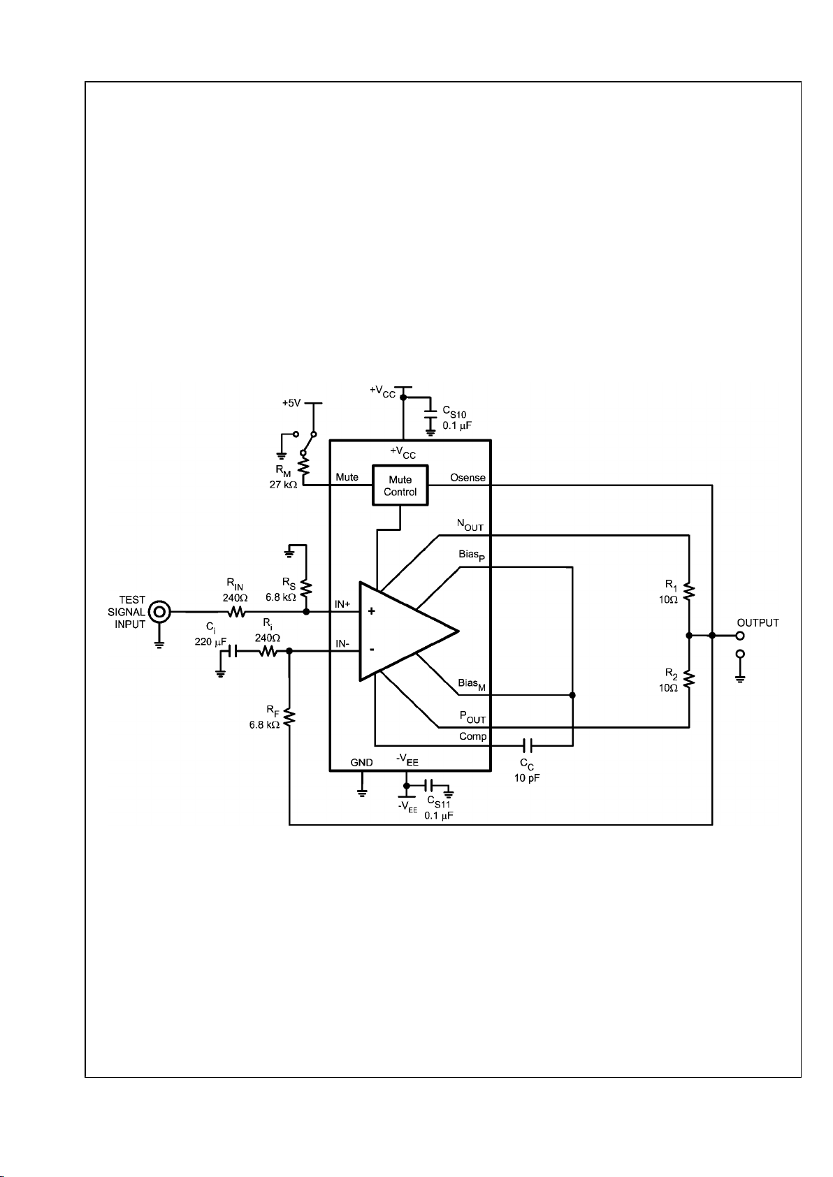
Test Circuit Diagram
30005093
FIGURE 3. LME49830 Test Circuit Diagram
www.national.com 6
LME49830
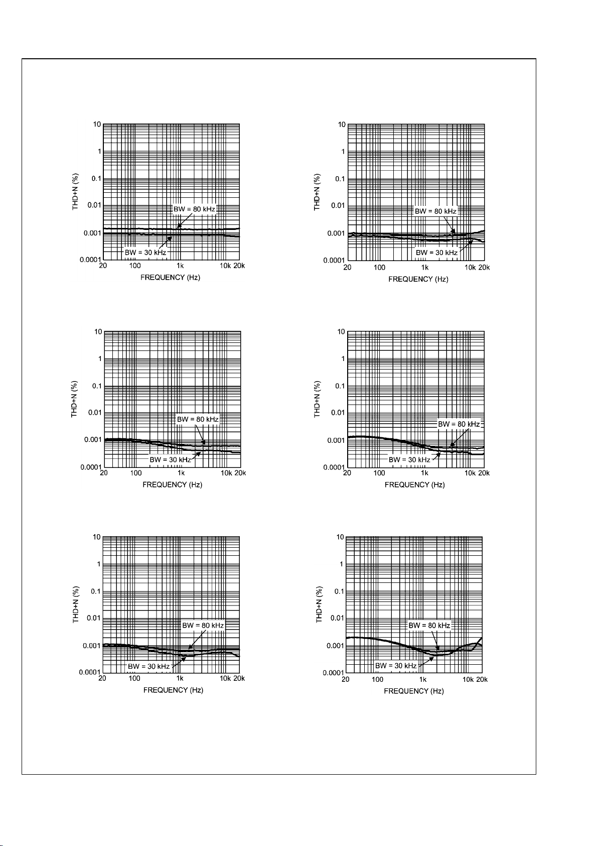
Typical Performance Characteristics
THD+N vs Frequency
+VCC = -VEE = 20V, VO = 5V
30005074
THD+N vs Frequency
+VCC = -VEE = 20V, VO = 10V
30005073
THD+N vs Frequency
+VCC = -VEE = 50V, VO = 14V
30005075
THD+N vs Frequency
+VCC = -VEE = 50V, VO = 20V
30005076
THD+N vs Frequency
+VCC = -VEE = 100V, VO = 14V
30005071
THD+N vs Frequency
+VCC = -VEE = 100V, VO = 30V
30005072
7 www.national.com
LME49830
 Loading...