

NSC LME49600TS, LME49600 Datasheet
February 7, 2008
LME49600
High Performance, High Fidelity, High Current Audio Buffer
General Description
The LME49600 is a high performance, low distortion high fidelity 250mA audio buffer. The LME49600 is designed for a
wide range of applications. It can be used inside the feedback
loop of op amps.
The LME49600 offers a pin-selectable bandwidth: a low current, 110MHz bandwidth mode that consumes 7.3mA and a
wide 180MHz bandwidth mode that consumes 13.2mA. In
both modes the LME49600 has a nominal 2000V/μs slew
rate. Bandwidth is easily adjusted by either leaving the BW
pin unconnected or connecting a resistor between the BW pin
and the VEE pin.
The LME49600 is fully protected through internal current limit
and thermal shutdown.
Key Specifications
■ Low THD+N
(V
OUT
= 3V
RMS
, f = 1kHz, Figure 2)
0.00003% (typ)
■ Slew Rate 2000V/μs (typ)
■ High Output Current 250mA (typ)
■ Bandwidth
BW pin floating 110MHz (typ)
BW connected to V
EE
180MHz (typ)
■ Supply Voltage Range ±2.25V ≤ V
S
≤ ±18V
Features
■
Pin-selectable bandwidth and quiescent current
■
Pure fidelity. Pure performance
■
Short circuit protection
■
Thermal shutdown
■
TO–263 surface-mount package
Applications
■
Headphone amplifier output drive stage
■
Line drivers
■
Low power audio amplifiers
■
High-current operational amplifier output stage
■
ATE Pin Driver Buffer
■
Power supply regulator
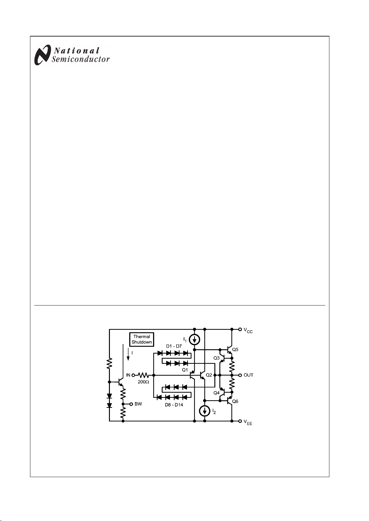
Functional Block Diagram
30029805
FIGURE 1. Simplified Circuit Diagram (Note: I1 and I2 are mirrored from I)
Boomer® is a registered trademark of National Semiconductor Corporation.
© 2008 National Semiconductor Corporation 300298 www.national.com
LME49600 High Performance, High Fidelity, High Current Audio Buffer
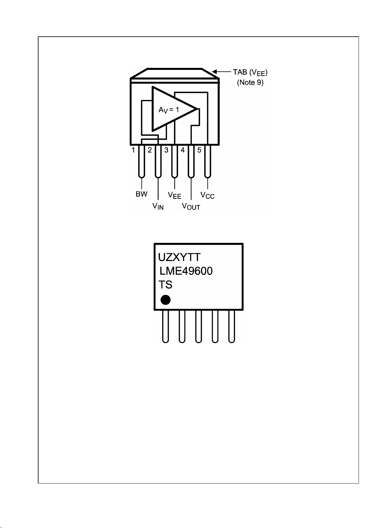
Connection Diagrams
300298a0
Top View
Order Number LME49600TS
See NS Package Number TS5B
30029832
Top View
U — Wafer fabrication code
Z — Assembly plant
XY — 2 Digit date code
TT — Lot traceability
www.national.com 2
LME49600
Absolute Maximum Ratings (Notes 1, 2)
If Military/Aerospace specified devices are required,
please contact the National Semiconductor Sales Office/
Distributors for availability and specifications.
Supply Voltage ±20V
ESD Ratings(Note 4) 2000V
ESD Ratings (Note 5) 200V
Storage Temperature −40°C to +150°C
Junction Temperature 150°C
Thermal Resistance
θ
JC
4°C/W
θ
JA
65°C/W
θJA (Note 3)
20°C/W
Soldering Information
TO-263 Package (10 seconds) 260°C
Operating Ratings (Notes 1, 2)
Temperature Range
T
MIN
≤ TA ≤ T
MAX
−40°C ≤ TA ≤ 85°C
Supply Voltage ±2.25V to ±18V
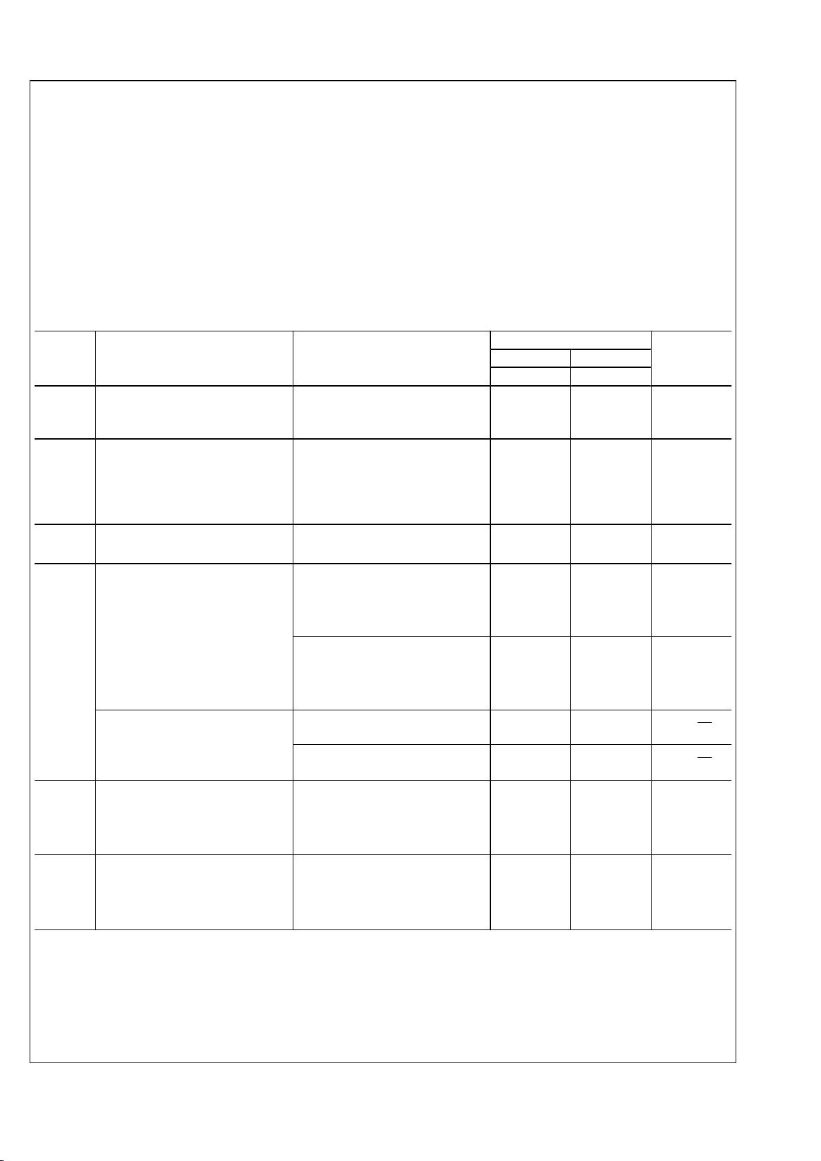
System Electrical Characteristics for LME49600 The following specifications apply for V
S
= ±15V,
fIN = 1kHz, unless otherwise specified. Typicals and limits apply for TA = 25°C.
Symbol Parameter Conditions
LME49600
Units
(Limits)
Typical Limit
(Note 6) (Note 7)
I
Q
Total Quiescent Current
I
OUT
= 0
BW pin: No connect
BW pin: Connected to VEE pin
7.3
13.2
10.5
18
mA (max)
mA (max)
THD+N
Total Harmonic Distortion + Noise
(Note 8)
AV = 1, V
OUT
= 3V
RMS
, R
L
= 32Ω, BW = 80kHz,
closed loop see Figure 2.
f = 1kHz
f = 20kHz
0.000035
0.0005
%
%
SR Slew Rate
30 ≤ BW ≤ 180MHz
V
OUT
= 20V
P-P
, RL = 100Ω
2000
V/μs
BW
Bandwidth
AV = –3dB
BW pin: No Connect
RL = 100Ω
RL = 1kΩ
100
110
MHz
MHz
AV = –3dB
BW pin: Connected to VEE pin
RL = 100Ω
RL = 1kΩ
160
180
MHz
MHz
Voltage Noise Density
f = 10kHz
BW pin: No Connect
3.0
nV/√Hz
f = 10kHz
BW pin: Connected to V
EE
pin
2.6
nV/√Hz
t
s
Settling Time
ΔV = 10V, RL = 100Ω
1% Accuracy
BW pin: No connect
BW pin: Connected to VEE pin
200
60
ns
ns
A
V
Voltage Gain
V
OUT
= ±10V
RL = 67Ω
RL = 100Ω
RL = 1kΩ
0.93
0.95
0.99
0.90
0.92
0.98
V/V (min)
V/V (min)
V/V (min)
3 www.national.com
LME49600
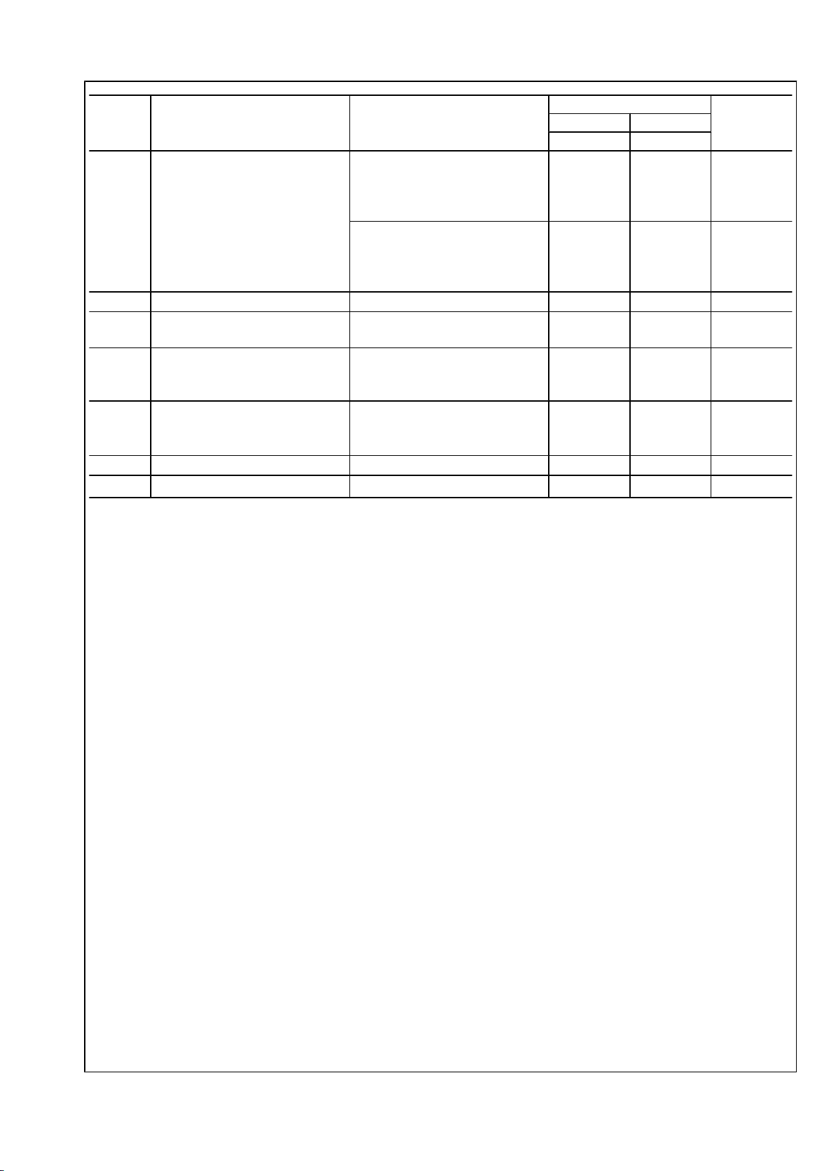
Symbol Parameter Conditions
LME49600
Units
(Limits)
Typical Limit
(Note 6) (Note 7)
V
OUT
Voltage Output
Positive
I
OUT
= 10mA
I
OUT
= 100mA
I
OUT
= 150mA
VCC –1.4
VCC –2.0
VCC –2.3
VCC –1.6
VCC –2.1
VCC –2.7
V (min)
V (min)
V (min)
Negative
I
OUT
= –10mA
I
OUT
= –100mA
I
OUT
= –150mA
VEE +1.5
VEE +3.1
VEE +3.5
VEE +1.6
VEE +2.4
VEE +3.2
V (min)
V (min)
V (min)
I
OUT
Output Current
±250 mA
I
OUT-SC
Short Circuit Output Current
BW pin: No Connect
BW pin: Connected to VEE pin
±490
±490
±550
mA (max)
mA (max)
I
B
Input Bias Current
VIN = 0V
BW pin: No Connect
BW pin: Connected to VEE pin
±1.0
±3.0
±2.5
±5.0
μA (max)
μA (max)
Z
IN
Input Impedance
RL = 100Ω
BW pin: No Connect
BW pin: Connected to VEE pin
7.5
5.5
MΩ
MΩ
V
OS
Offset Voltage ±17 ±60 mV (max)
VOS/°C
Offset Voltage vs Temperature
40°C ≤ TA ≤ +125°C
±100
μV/°C
Note 1: All voltages are measured with respect to ground, unless otherwise specified.
Note 2: Absolute Maximum Ratings indicate limits beyond which damage to the device may occur. Operating Ratings indicate conditions for which the device is
functional, but do not guarantee specific performance limits. Electrical Characteristics state DC and AC electrical specifications under particular test conditions
which guarantee specific performance limits. This assumes that the device is within the Operating Ratings. Specifications are not guaranteed for parameters
where no limit is given, however, the typical value is a good indication of device performance.
Note 3: The maximum power dissipation must be derated at elevated temperatures and is dictated by T
JMAX
, θJA, and the ambient temperature TA. The maximum
allowable power dissipation is P
DMAX
= (T
JMAX–TA
)/θJA or the number given in Absolute Maximum Ratings, whichever is lower. For the LME49600, typical
application (shown in Figure 2) with V
SUPPLY
= 30V, RL = 32Ω, the total power dissipation is 1.9W. θJA = 20°C/W for the TO–263 package mounted to 16in2 1oz
copper surface heat sink area.
Note 4: Human body model, 100pF discharged through a 1.5kΩ resistor.
Note 5: Machine Model, 220pF – 240pF discharged through all pins.
Note 6: Typical specifications are specified at 25°C and represent the parametric norm.
Note 7: Tested limits are guaranteed to National's AOQL (Average Outgoing Quality Level).
Note 8: This is the distortion of the LME49600 operating in a closed loop configuration with an LME49710. When operating in an operational amplifier's feedback
loop, the amplifier’s open loop gain dominates, linearizing the system and determining the overall system distortion.
Note 9: The TSB package is non-isolated package. The package's metal back and any heat sink to which it is mounted are connected to the same potential as
the -VEE pin.
www.national.com 4
LME49600
Typical Performance Characteristics
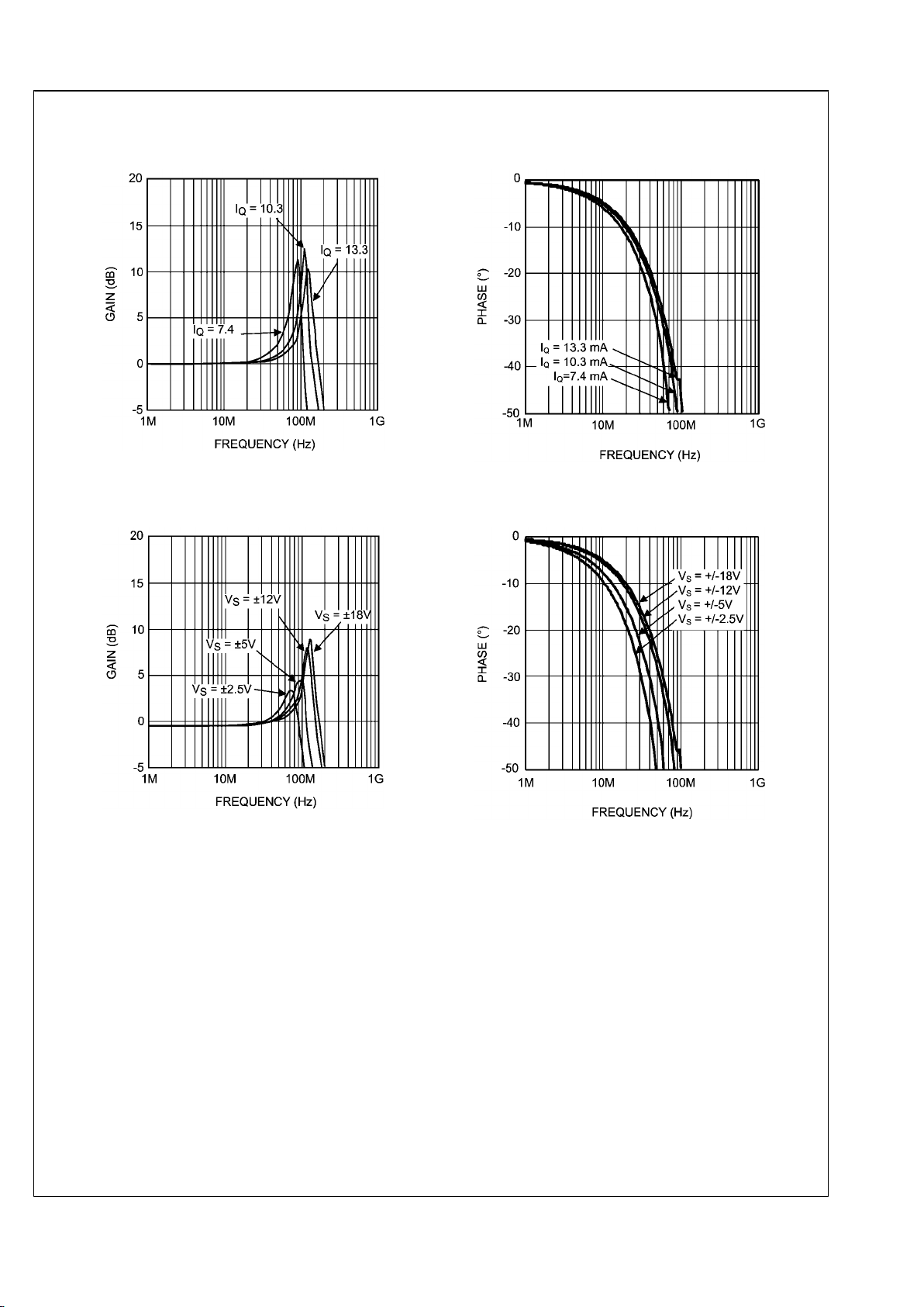
Gain vs Frequency vs Quiescent Current
30029899
Phase vs Frequency vs Quiescent Current
30029881
Gain vs Frequency vs Power Supply Voltage
Wide BW Mode
30029898
Phase vs Frequency vs Supply Voltage
Wide BW Mode
30029880
5 www.national.com
LME49600
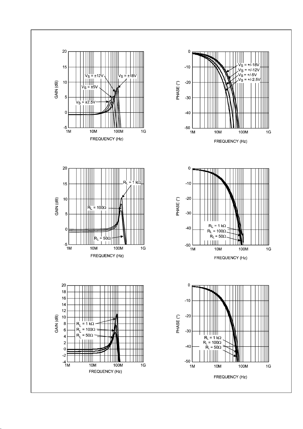
Gain vs Frequency vs Power Supply Voltage
Low IQ Mode
30029897
Phase vs Frequency vs Supply Voltage
Low IQ Mode
30029879
Gain vs Frequency vs R
LOAD
Wide BW Mode
30029896
Phase vs Frequency vs R
LOAD
Wide BW Mode
30029878
Gain vs Frequency vs R
LOAD
Low IQ Mode
30029895
Phase vs Frequency vs R
LOAD
Low IQ Mode
30029877
www.national.com 6
LME49600
 Loading...