

LMD18245
3A, 55V DMOS Full-Bridge Motor Driver
LMD18245 3A, 55V DMOS Full-Bridge Motor Driver
April 1998
General Description
The LMD18245 full-bridge power amplifier incorporates all
the circuit blocks required to drive and control current in a
brushed type DC motor or one phase of a bipolar stepper
motor.The multi-technology process used tobuild thedevice
combines bipolar and CMOS control and protection circuitry
with DMOS power switches on the same monolithic structure. The LMD18245 controls the motor current via a fixed
off-time chopper technique.
An all DMOS H-bridge power stage delivers continuous output currents up to3A (6A peak)at supplyvoltages up to 55V.
The DMOS power switches feature low R
ficiency, and a diode intrinsic to the DMOS body structure
eliminates the discrete diodes typically required to clamp bipolar power stages.
An innovative current sensing method eliminates the power
loss associated witha senseresistor in serieswith themotor.
Afour-bit digital-to-analog converter (DAC) provides a digital
path for controllingthe motorcurrent, and, by extension, simplifies implementationof full, half and microstep stepper motor drives. For higher resolution applications, an external
DAC can be used.
DS(ON)
for high ef-
Features
n DMOS power stage rated at 55V and 3A continuous
n Low R
n Internal clamp diodes
n Low-loss current sensing method
n Digital or analog control of motor current
n TTL and CMOS compatible inputs
n Thermal shutdown (outputs off) at T
n Overcurrent protection
n No shoot-through currents
n 15-lead TO-220 molded power package
of typically 0.3Ω per power switch
DS(ON)
=
155˚C
J
Applications
n Full, half and microstep stepper motor drives
n Stepper motor and brushed DC motor servo drives
n Automated factory, medical and office equipment
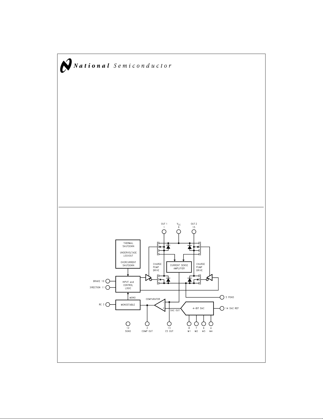
Functional Block and Connection Diagram (15-Lead TO-220 Molded Power Package (T) )
DS011878-1
Order Number LMD18245T
See NS Package Number TA15A
© 1998 National Semiconductor Corporation DS011878 www.national.com

Absolute Maximum Ratings (Note 1)
If Military/Aerospace specified devices are required,
please contact the National Semiconductor Sales Office/
Distributors for availability and specifications.
DC Voltage at:
OUT 1, V
COMP OUT, RC, M4, M3, M2, M1, BRAKE, +12V
DIRECTION, CS OUT, and DAC REF
DC Voltage PGND to SGND
Continuous Load Current 3A
Peak Load Current (Note 2) 6A
Junction Temperature (T
, and OUT 2 +60V
CC
±
) +150˚C
J(max)
400mV
Power Dissipation (Note 3) :
TO-220 (T
TO-220 (T
=
25˚C, Infinite Heatsink) 25W
A
=
25˚C, Free Air) 3.5W
A
ESD Susceptibility (Note 4) 1500V
Storage Temperature Range (T
) −40˚C to +150˚C
S
Lead Temperature (Soldering, 10 seconds) 300˚C
Operating Conditions (Note 1)
Temperature Range (T
Supply Voltage Range (V
CS OUT Voltage Range 0V to +5V
DAC REF Voltage Range 0V to +5V
) (Note 3) −40˚C to +125˚C
J
) +12V to +55V
CC
MONOSTABLE Pulse Range 10 µs to 100 ms
Electrical Characteristics (Note 2)
The following specifications apply for V
perature range, −40˚C ≤ T
≤ +125˚C. All other limits apply for T
J
Symbol Parameter Conditions Typical Limit Units
I
CC
Quiescent Supply Current DAC REF=0V, V
POWER OUTPUT STAGE
R
V
T
Q
t
D(ON)
DS(ON)
DIODE
rr
rr
Switch ON Resistance I
Body Diode Forward Voltage I
Diode Reverse Recovery Time I
Diode Reverse Recovery Charge I
Output Turn ON Delay Time
Sourcing Outputs I
Sinking Outputs I
t
D(OFF)
Output Turn OFF Delay Time
Sourcing Outputs I
Sinking Outputs I
t
ON
Output Turn ON Switching Time
Sourcing Outputs I
Sinking Outputs I
t
OFF
Output Turn OFF Switching Time
Sourcing Outputs I
Sinking Outputs I
t
pw
t
DB
Minimum Input Pulse Width Pins 10 and 11 2 µs
Minimum Dead Band (Note 6) 40 ns
CURRENT SENSE AMPLIFIER
Current Sense Output I
Current Sense Linearity Error 0.5A ≤ I
Current Sense Offset I
=
+42V, unless otherwise stated. Boldface limits apply over the operating tem-
CC
=
=
T
25˚C.
A
J
(Note 5) (Note 5) (Limits)
=
+20V 8 mA
CC
15 mA (max)
=
3A 0.3 0.4 Ω (max)
LOAD
0.6 Ω (max)
=
I
6A 0.3 0.4 Ω (max)
LOAD
0.6 Ω (max)
=
3A 1.0 V
DIODE
1.5 V(max)
=
1A 80 ns
DIODE
=
1A 40 nC
DIODE
=
3A 5 µs
LOAD
=
3A 900 ns
LOAD
=
3A 600 ns
LOAD
=
3A 400 ns
LOAD
=
3A 40 µs
LOAD
=
3A 1 µs
LOAD
=
3A 200 ns
LOAD
=
3A 80 ns
LOAD
=
1A (Note 7) 200 µA (min)
LOAD
250 175 µA (min)
300 µA (max)
325 µA (max)
≤ 3A (Note 7)
LOAD
=
0A 5 µA
LOAD
±
6
±
9
20 µA (max)
%
(max)
%
www.national.com 2

Electrical Characteristics (Note 2) (Continued)
The following specifications apply for V
perature range, −40˚C ≤ T
≤ +125˚C. All other limits apply for T
J
Symbol Parameter Conditions Typical Limit Units
DIGITAL-TO-ANALOG CONVERTER (DAC)
Resolution 4 Bits (min)
Monotonicity 4 Bits (min)
Total Unadjusted Error 0.125 0.25 LSB (max)
Propagation Delay 50 ns
I
REF
DAC REF Input Current DAC REF=+5V −0.5 µA
COMPARATOR AND MONOSTABLE
Comparator High Output Level 6.27 V
Comparator Low Output Level 88 mV
Comparator Output Current
Source 0.2 mA
Sink 3.2 mA
t
DELAY
Monostable Turn OFF Delay (Note 8) 1.2 µs
PROTECTION AND PACKAGE THERMAL RESISTANCES
Undervoltage Lockout, V
T
JSD
Shutdown Temperature, T
Package Thermal Resistances
θ
JC
θ
JA
Junction-to-Case, TO-220 1.5 ˚C/W
Junction-to-Ambient, TO-220 35 ˚C/W
LOGIC INPUTS
V
IL
V
IH
I
IN
Note 1: Absolute Maximum Ratings indicate limits beyond which damage to the devicemay occur. Electrical specifications do notapply when operating the device
outside the rated Operating Conditions.
Note 2: Unless otherwise stated, load currents are pulses with widths less than 2 ms and duty cycles less than 5%.
Note 3: The maximum allowable powerdissipation at any ambient temperature is P
eration, T
ing T
junction-to-case thermal resistance of the package, θ
Note 4: ESDrating is based on thehuman body model of 100 pFdischarged through a 1.5 kΩ resistor.M1,M2,M3 and M4, pins 8,7, 6 and 4 are protectedto 800V.
Note 5: All limits are 100%production tested at 25˚C. Temperature extreme limits are guaranteed via correlation using accepted SQC (Statistical Quality Control)
methods. All limits are used to calculate AOQL (Average Outgoing Quality Level). Typicals are at T
Note 6: Asymmetric turn OFF and ON delay times and switching times ensure a switch turns OFF before the other switch in the same half H-bridge begins to turn
ON (preventing momentary short circuits between the power supply and ground). The transitional period during which both switches are OFF is commonly referred
to as the dead band.
Note 7: (I
The current sense linearity is specified as the slope of the line between the 0.5A and 1Adata points minus the slope of the line between the 2A and 3Adata points
all divided by the slope of the line between the 0.5A and 1A data points.
Note 8: Turn OFF delay, t
DMOS switch beginning to turn OFF. With V
5V at 1.2V/µs, and t
Low Level Input Voltage −0.1 V (min)
High Level Input Voltage 2 V (min)
Input Current V
is the ambient temperaturein ˚C, and θJAis the junction-to-ambient thermalresistance in ˚C/W. Exceeding P
A
above 125˚C. If the junction temperature exceeds 155˚C, internal circuitry disables the power bridge. When a heatsink is used, θJAis the sum of the
J
LOAD,ISENSE
) data points are taken for load currents of 0.5A, 1A, 2A and 3A. The current sense gain is specified as I
, is defined as the time from the voltage at the output of the current sense amplifier reaching the DAC output voltage to the lower
DELAY
is measured as the time from the voltage at RC reaching 2V to the time the voltage at OUT 1 reaches 3V.
DELAY
=
+42V, unless otherwise stated. Boldface limits apply over the operating tem-
CC
CC
J
=
0V or 12V
IN
, and the case-to-ambient thermal resistance of the heatsink.
JC
=
32V, DIRECTION high, and 200Ω connected between OUT1 and V
CC
A
Max
=
=
T
25˚C.
J
=
)/θJA, where 125˚Cis the maximum junction temperature for op-
(125 − T
A
=
J
(Note 5) (Note 5) (Limits)
0.5 LSB (max)
±
10 µA (max)
2.0 µs (max)
5 V (min)
8 V (max)
155 ˚C
0.8 V (max)
12 V (max)
±
10 µA (max)
voids the Electrical Specificationsby forc-
max
25˚C and represent the most likely parametric norm.
SENSE/ILOAD
, the voltage at RC is increased from 0V to
CC
for the 1A data point.
3 www.national.com
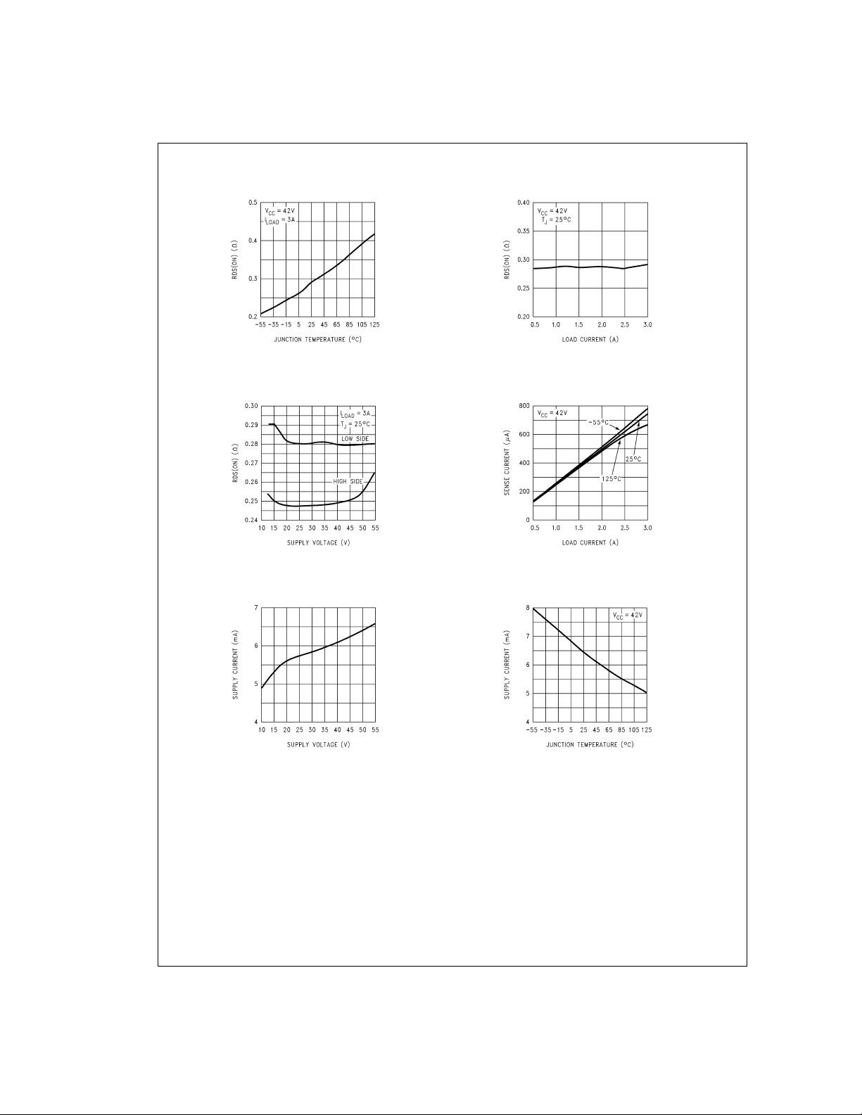
Typical Performance Characteristics
RDS(ON) vs Temperature
RDS(ON) vs
Supply Voltage
Supply Current vs
Supply Voltage
DS011878-29
DS011878-31
RDS(ON) vs Load Current
DS011878-30
Current Sense Output
vs Load Current
DS011878-32
Supply Current vs
Temperature
DS011878-33
www.national.com 4
DS011878-34
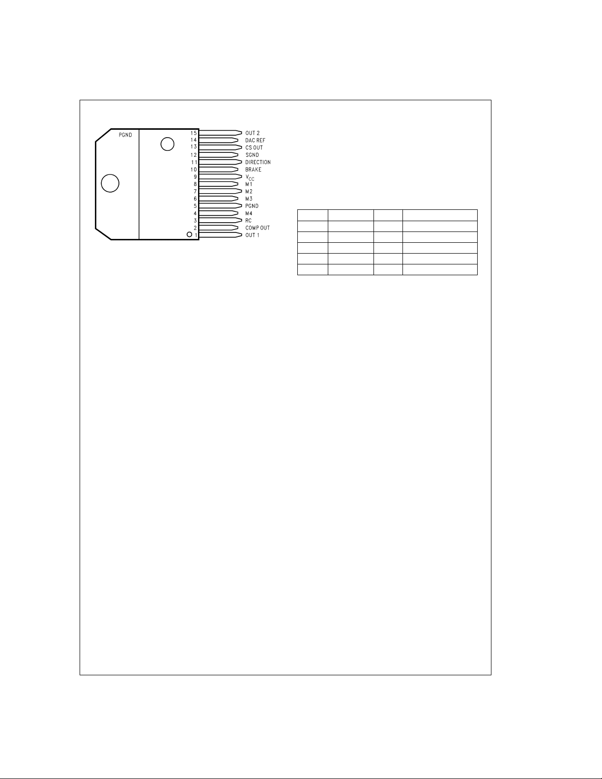
Connection Diagram
DS011878-2
15-Lead TO-220 Molded Power Package
See NS Package Number TA15A
Pinout Descriptions
and Connection Diagrams)
Pin 1, OUT 1: Output node of the first half H-bridge.
Pin 2, COMP OUT: Output of the comparator. If the voltage
at CS OUT exceeds that providedby theDAC, the comparator triggers the monostable.
Pin 3, RC: Monostable timing node. A parallel resistorcapacitor network connected between this node and ground
sets the monostable timing pulse at about 1.1 RC seconds.
Pin 5, PGND: Ground return node ofthe powerbridge. Bond
wires (internaI) connect PGND to the tab of the TO-220
package.
Pins 4 and 6 through 8, M4 through M1: Digital inputs of
the DAC. These inputs make up a four-bit binary number
with M4 as the most significant bit or MSB. The DAC provides an analog voltage directly proportional to the binary
number applied at M4 through M1.
Pin 9, V
Pin 10, BRAKE: Brake logic input. Pulling the BRAKE input
logic-high activates both sourcing switches of the power
bridge—effectively shorting the load. See
the load in this manner forces the load current to recirculate
and decay to zero.
Pin 11, DIRECTION: Direction logic input. The logic level at
this input dictates the direction of current flow in the load.
See
Pin 12, SGND: Ground returnnode of allsignal levelcircuits.
: Power supply node.
CC
Table 1
.
Top View
Order Number LMD18245T
(See Functional Block
Table 1
. Shorting
Pin 13, CS OUT: Output of the current sense amplifier. The
current sense amplifier sources 250 µA(typical) per ampere
of totalforward current conducted by the upper two switches
of the power bridge.
Pin 14, DAC REF: Voltage reference input of the DAC. The
DAC provides an analog voltage equal to V
where D is the decimal equivalent (0–15) of the binary num-
DAC REF
x D/16,
ber applied at M4 through M1.
Pin 15, OUT 2: Output node of the second half H-bridge.
TABLE 1. Switch Control Logic Truth Table
BRAKE DIRECTION MONO Active Switches
H X X Source 1, Source 2
L H L Source 2
L H H Source 2, Sink 1
L L L Source 1
L L H Source 1, Sink 2
X=don’t care
MONO is the output of the monostable.
Functional Descriptions
TYPICAL OPERATION OF A CHOPPER AMPLIFIER
Chopper amplifiers employ feedback driven switching of a
power bridge to control and limit current in the winding of a
motor (
Figure 1
power switches and four diodes connected in an H configuration. Control circuitry (not shown) monitors the winding
current and compares it to a threshold. While the winding
current remainsless than the threshold, a source switch and
a sink switch in opposite halves of the bridge force the supply voltage across the winding, and the winding current increases rapidly towards V
As the winding current surpasses the threshold, the control
circuitry turns OFF the sink switch for a fixed period or
off-time.
site upper diode short the winding, and the winding current
recirculates and decays slowly towards zero (
Figure 1e
turns back ON the sink switch, and the winding current again
increases rapidly towards V
again). The above sequence repeats to provide a current
chopping action that limits the winding current to the threshold (
Figure 1g
reaches the threshold. During a change in the direction of
the winding current, the diodes provide a decay path for the
initial winding current (
bridge shorts the winding fora fixed period, this typeof chopper amplifier is commonly referred to as a
chopper.
). The bridge consists of four solid state
/R (
CC
Figure 1a
and
Figure 1d
During the off-time, the source switch and the oppo-
Figure 1b
and
). At the end of the off-time, the control circuitry
/R (
CC
Figure 1a
and
Figure 1d
). Chopping only occurs if the winding current
Figure 1c
and
Figure 1f
). Since the
fixed off-time
).
5 www.national.com
Functional Descriptions (Continued)
(a)
(c)
(e)
DS011878-3
DS011878-5
(b)
DS011878-4
(d)
DS011878-6
(f)
DS011878-7
DS011878-8
(g)
DS011878-9
FIGURE 1. Chopper Amplifier Chopping States: Full VCCApplied Across the Winding (a) and (d), Shorted Winding (b)
and (e), Winding Current Decays During a Change in the Direction of the Winding Current (c) and (f), and the
Chopped Winding Current (g)
www.national.com 6
 Loading...