

LMC835 Digital Controlled Graphic Equalizer
LMC835 Digital Controlled Graphic Equalizer
February 1995
General Description
The LMC835 is a monolithic, digitally-controlled graphic
equalizer CMOS LSI for Hi-Fi audio. The LMC835 consists
of a Logic section and a Signal Path section made of analog
switches and thin-film silicon-chromium resistor networks.
The LMC835 is used with external resonator circuits to
make a stereo equalizer with seven bands,
g
12 dB org6
dB gain range and 25 steps each. Only three digital inputs
are needed to control the equalization. The LMC835 makes
it easy to build a mP-controlled equalizer.
The signal path is designed for very low noise and distortion, resulting in very high performance, compatible with
PCM audio.
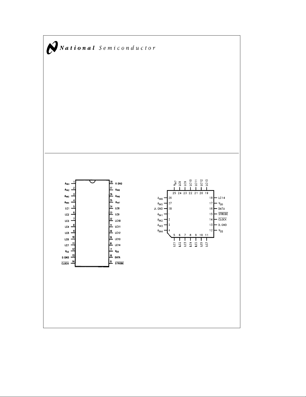
Connection Diagrams
Dual-In-Line Package
Features
Y
No volume controls required
Y
Three-wire interface
Y
14 bands, 25 steps each
Y
g
12 dB org6 dB gain ranges
Y
Low noise and distortion
Y
TTL, CMOS logic compatible
Applications
Y
Hi-Fi equalizer
Y
Receiver
Y
Car stereo
Y
Musical instrument
Y
Tape equalization
Y
Mixer
Y
Volume controller
Molded Chip Carrier Package
Top View
TL/H/6753– 26
Order Number LMC835V
See NS Package V28A
Top View
TL/H/6753– 1
Order Number LMC835N
See NS Package N28B
C
1995 National Semiconductor Corporation RRD-B30M75/Printed in U. S. A.
TL/H/6753
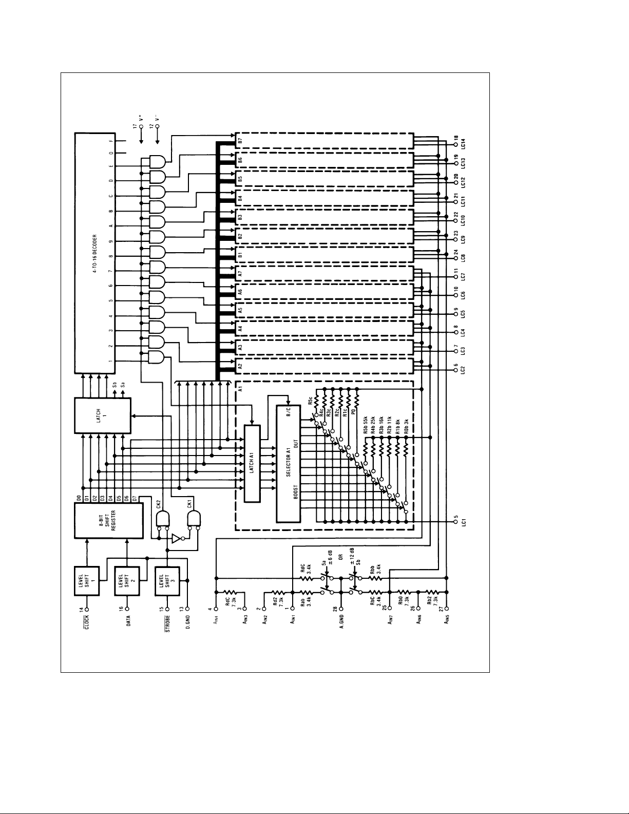
Block Diagram
TL/H/6753– 2
2
Absolute Maximum Ratings
If Military/Aerospace specified devices are required,
please contact the National Semiconductor Sales
Office/Distributors for availability and specifications.
Supply Voltage, V
Allowable Input Voltage (Note 1) V
Storage Temperature, T
Lead Temperature (Soldering, 10 sec), N Pkg
Lead Temperature, V Pkg
Vapor Phase (60 sec)
Infrared (15 sec)
DD
b
V
SS
b
stg
60§Ctoa150§C
to V
DD
SS
a
a
a
18V
b
0.3V
a
0.3V
260§C
215§C
220§C
Operating Ratings
Supply Voltage, V
Digital Ground (Pin 13) VSSto V
Digital Input (Pins 14, 15, 16) VSSto V
Analog Input (Pins 1, 2, 3, 4, 25, 26, 27)
(Note 1) V
Operating Temperature, T
DD
b
V
SS
opr
5V to 16V
SS
b
40§Ctoa85§C
to V
DD
DD
DD
Electrical Characteristics (Note 2) V
LOGIC SECTION
DD
e
7.5V, V
eb
7.5V, A.GNDe0V
SS
Tested Design
Symbol Parameter Test Conditions Typ Limit Limit
(Note 3) (Note 4)
I
DDL
I
SSL
I
DDH
I
SSH
V
IH
V
IL
f
o
t
w(STB)
t
setup
t
hold
t
cs
I
IN
C
IN
Note 1: Pins 2, 3 and 26 have a maximum input voltage range ofg22V for the typical application shown in
Note 2: Bold numbers apply at temperature extremes. All other numbers apply at T
circuit,
Note 3: Guaranteed and 100% production tested.
Note 4: Guaranteed (but not 100% production tested) over the operating temperature range. These limits are not used to calculate outgoing quality levels.
Supply Current Pins 14, 15, 16 are 0V 0.01 0.5 0.5 mA (Max)
Pins 14, 15, 16 are 0V 0.01 0.5 0.5 mA (Max)
Pins 14, 15, 16 are 5V 1.3 5 5 mA (Max)
Pins 14, 15, 16 are 5V 0.9 5 5 mA (Max)
High-Level Input Voltage
Low-Level Input Voltage
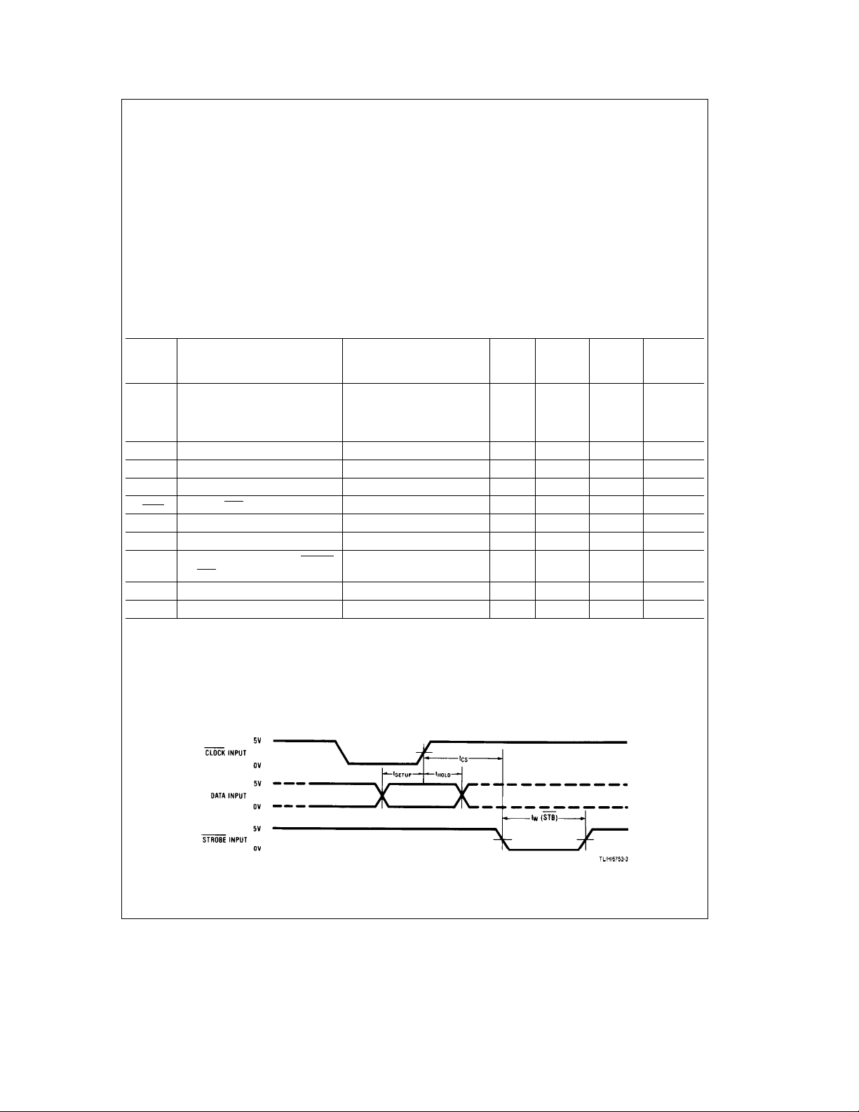
Clock Frequency
Width of STB Input See
Data Setup Time See
Data Hold Time See
Delay from Rising Edge of CLOCK See
@
Pins 14, 15, 16 1.8 2.3 2.5 V (Min)
@
Pins 14, 15, 16 0.9 0.6 0.4 V (Max)
@
Pin 14 2000 500 500 kHz (Max)
Figure 1
Figure 1
Figure 1
Figure 1
0.25 1 1 ms (Min)
0.25 1 1 ms (Min)
0.25 1 1 ms (Min)
0.25 1 1 ms (Min)
to STB
A
e
25§C, V
k
5Vg0.01
IN
e
7.5V, V
DD
g
1 mA (Max)
Figure 7
.
eb
7.5V,D.GNDeA.GNDe0V as shown in the test
SS
Input Current
Input Capacitance
Figures 3
and4.
@
Pins 14, 15, 16 0VkV
@
Pins 14, 15, 16 fe1 MHz 5 pF
Timing Diagram
Unit
(Limit)
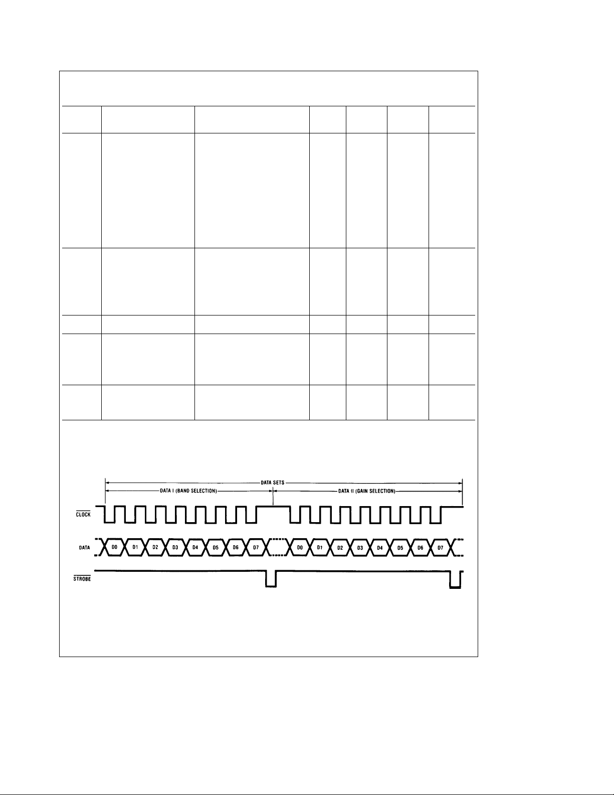
Note: To change the gain of the presently selected band, it is not necessary to send DATA 1 (Band Selection) each time.
FIGURE 1
3
TL/H/6753– 3
Electrical Characteristics (Note 2) V
DD
e
7.5V, V
eb
7.5V, D.GNDeA.GNDe0V
SS
SIGNAL PATH SECTION
Symbol Parameter Test Conditions Typ Limit Limit
@
E
A
THD Total Harmonic A
V
O Max
Gain Error A
Distortion V
Maximum Output Voltage A
S/N Signal to Noise Ratio A
I
LEAK
Note 2; Boldface numbers apply at temperature extremes. All other numbers apply at T
test circuit,
Note 3: Guaranteed and 100% production tested.
Note 4: Guaranteed (but not 100% production tested) over the operating temperature range. These limits are not used to calculate outgoing quality levels.
Leakage Current A
Figures 3
and4.
e
V
e
A
V
e
A
V
(R
e
A
V
(R4bor R4cis ON)
e
A
V
(R
e
A
V
(R
e
A
V
(R
e
A
V
(R
e
V
e
A
V
V
V
eb
A
V
V
V
e
V
THD
e
V
V
e
A
V
V
eb
A
V
V
e
V
(All internal switches are OFF)
Pin 2
Pin 5EPin 11, Pin 18EPin 24 50 nA (Max)
g
0dB
0dB
g
5b
g
g
3b
g
2b
g
1b
g
0b
0dB
IN
12 dB
IN
IN
IN
IN
0dB
0dB
ref
ref
ref
0dB
e
e
e
e
e
12 dB
12 dB Range 0.1 0.5 0.5 dB (Max)
@
g
6 dB Range 0.1 1 1 dB (Max)
@
g
1dB
or R5cis ON)
2dB
3dB
or R3cis ON)
4dB
or R2cis ON)
5dB
or R1cis ON)
9dB
or R0cis ON)
12 dB
k
e
e
12 dB
e
a
dB Range 0.1 0.5 0.6 dB (Max)
@
g
12 dB Range 0.1 0.5 0.6 dB (Max)
@
g
12 dB Range 0.1 0.5 0.6 dB (Max)
@
g
12 dB Range 0.1 0.5 0.7 dB (Max)
@
g
12 dB Range 0.1 0.5 0.7 dB (Max)
@
g
12 dB Range 0.2 1 1.3 dB (Max)
@
g
12 dB Range 0.0015 %
4V
,fe1 kHz
rms
@
g
12 dB Range
1V
,fe1 kHz 0.01 0.1 % (Max)
rms
1V
,fe20 kHz 0.1 0.5 % (Max)
rms
@
g
4V
4V
1V
1V
1V
12 dB Range
,fe1 kHz 0.01 0.1 % (Max)
rms
,fe20 kHz 0.1 0.5 % (Max)
rms
@
g
12 dB Range 5.5 5.1 5 V
1%, fe1 kHz
@
g
12 dB Range 114 dB
rms
@
g
12 dB Range 106 dB
rms
@
g
12 dB Range 116 dB
rms
@
g
12 dB Range
3, Pin 26 500 nA (Max)
e
A
25§C, V
e
DD
Tested Design
(Note 3) (Note 4)
eb
7.5V, V
SS
rms
7.5V, D.GNDeA.GNDe0V as shown in the
Unit
(Limit)
(Min)
Timing Diagrams
Note: To change the gain of the presently selected band, it is not necessary to send DATA 1 (Band Selection) each time.
FIGURE 2
4
TL/H/6753– 4
Truth Tables
DATA I (Band Selection)
D7 D6 D5 D4 D3 D2 D1 D0
HXLLLLLL
HXLLLLLH
HXLLLLHL
HXLLLLHH
HXLL LHLL
HXLL LHLH
HXLL LHHL
HX L L L HHH
HXLLHLLL
HXLLHL LH
HXLLHLHL
HXLLHLHH
HXLLHHLL
HXLLHHLH
HX L LHHHL
HX L LHHHH
H X L H Valid Binary Input
H X H L Valid Binary Input
H X H H Valid Binary Input
w
uuuu
jklm
j
DATA 1
k Don’t Care
g
l Ch A
m Ch B
6 dB/g12 dB Range
g
6 dB/g12 dB Range
Band Code
x
(Ch A: Band 1E7, Ch B: Band 8E14)
g
Ch A
12 dB Range, Ch Bg12 dB Range, No Band Selection
g
Ch A
12 dB Range, Ch Bg12 dB Range, Band 1
g
Ch A
12 dB Range, Ch Bg12 dB Range, Band 2
g
Ch A
12 dB Range, Ch Bg12 dB Range, Band 3
g
Ch A
12 dB Range, Ch Bg12 dB Range, Band 4
g
Ch A
12 dB Range, Ch Bg12 dB Range, Band 5
g
Ch A
12 dB Range, Ch Bg12 dB Range, Band 6
g
Ch A
12 dB Range, Ch Bg12 dB Range, Band 7
g
Ch A
12 dB Range, Ch Bg12 dB Range, Band 8
g
Ch A
12 dB Range, Ch Bg12 dB Range, Band 9
g
Ch A
12 dB Range, Ch Bg12 dB Range, Band 10
g
Ch A
12 dB Range, Ch Bg12 dB Range, Band 11
g
Ch A
12 dB Range, Ch Bg12 dB Range, Band 12
g
Ch A
12 dB Range, Ch Bg12 dB Range, Band 13
g
Ch A
12 dB Range, Ch Bg12 dB Range, Band 14
g
Ch A
12 dB Range, Ch Bg12 dB Range, No Band Selection
g
Ch A
12 dB Range, Ch Bg6 dB Range, Band 1E14
g
Ch A
6 dB Range, Ch Bg12 dB Range, Band 1E14
g
Ch A
6 dB Range, Ch Bg6 dB Range, Band 1E14
g
This is the gain if the
selected by DATA I. If the
range is selected, then the values
shown must be approximately halved.
See the characteristics curves for
more exact data.
12 dB range is
g
6dB
DATA II (Gain Selection)
D7 D6 D5 D4 D3 D2 D1 D0
Flat L X L L L L L L
1 dB Boost L H H L L L L L
2 dB Boost L H L H L L L L
3 dB Boost L H L L H L L L
4 dB Boost L H L L L H L L
5 dB Boost L H L L L L H L
6 dB Boost L H L H L L H L
7 dB Boost L H H L H L H L
8 dB Boost L H L H L H H L
9 dB Boost L H L L L L L H
10 dB Boost L H H L H L L H
11 dB Boost L H H L H H L H
12 dB Boost L H H L H H H H
E
$1dB
n
o Boost/Cut
12 dB Cut L L
DATA II
5
uu
no
Valid Above Input
w
Gain Code
x
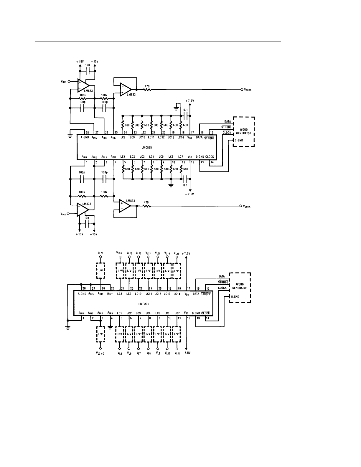
Test Circuits
FIGURE 3. Test Circuit for AC Measurement
FIGURE 4. Test Circuit for Leakage Current Measurement
6
TL/H/6753– 5
TL/H/6753– 6
 Loading...