

LMC8101
Rail-to-Rail Input and Output, 2.7V Op Amp in
micro SMD package with Shutdown
LMC8101 Rail-to-Rail Input and Output, 2.7V Op Amp in micro SMD package with Shutdown
September 1999
General Description
The LMC8101 is a Rail-to-Rail Input and Output high performance CMOS operational amplifier. The LMC8101 is ideal
for low voltage (2.7V to 10V) applications requiring
Rail-to-Rail inputs and output. The LMC8101 is supplied in
the die sized micro SMD as well as the 8 pin MSOP packages. The micro SMD package requires 75%less board
space as comparedto the SOT23-5 package. The LMC8101
is an upgrade to the industry standard LMC7101.
The LMC8101 incorporates a simple user controlled methodology for shutdown. This allows ease of use while reducing
the total supply current to 1nA typical. This extends battery
life where power saving is mandated. The shutdown input
threshold can be set relative to either V
pin (see Application Note section for details).
Other enhancements include improved offset voltage limit,
three times the output current drive and lower 1/f noise when
compared to the industry standard LMC7101 Op Amp. This
makes the LMC8101 ideal for use in many battery powered,
wireless communication and Industrial applications.
+
or V−using the SL
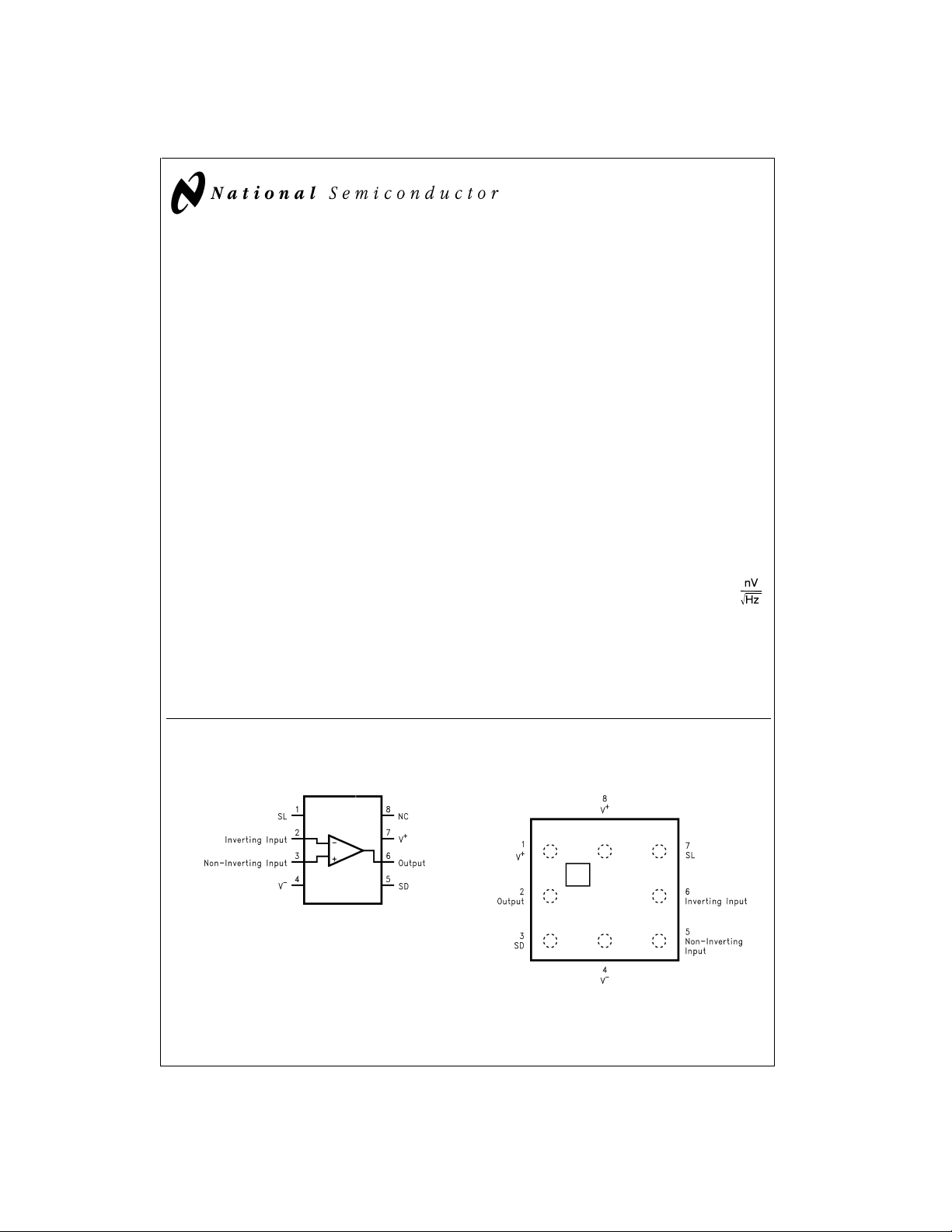
Connection Diagrams
8-Pin MSOP
Features
=
V
2.7V, T
S
specified.
n Rail-to-Rail Inputs
n Rail-to-Rail Output
Swing Within 35mV of Supplies (R
n Packages Offered:
n micro SMD package 1.39mm x 1.41mm
n MSOP package 3.0mm x 4.9mm
n Low Supply Current
n Shutdown Current 1µA (max)
n Versatile Shutdown feature 10µs turn-on
n Output Short Circuit Current 10mA
n Offset Voltage
n Gain-Bandwidth 1MHz
n Supply Voltage Range 2.7V-10V
n THD 0.18
n Voltage Noise 36
A
=
25˚C, R
to V+/2, Typical values unless
L
L
<
1mA (max)
±
5 mV (max)
=
2kΩ)
Applications
n Portable Communication (voice, data)
n Cellular Phone Power Amp Control Loop
n Buffer AMP
n Active Filters
n Battery Sense
n VCO Loop
micro SMD
%
DS101240-79
Top View
DS101240-80
Top View
© 1999 National Semiconductor Corporation DS101240 www.national.com
Ordering Information
Package Ordering Information NSC Drawing
micro SMD
8-Pin MSOP
LMC8101BP
LMC8101BPX 3k Units Tape and Reel
LMC8101MM
LMC8101MMX 3.5k Units Tape and Reel
Number
BPA08EFB
MUA08A A11
Package
Marking
A
2
Supplied As
250 Units Tape and Reel
1k Units Tape and Reel
www.national.com 2
Absolute Maximum Ratings (Note 1)
If Military/Aerospace specified devices are required,
please contact the National Semiconductor Sales Office/
Distributors for availability and specifications.
ESD Tolerance 2KV (Note 2)
differential +/−Supply Voltage
V
IN
Output Short Circuit Duration (Notes 3, 11)
Supply Voltage (V
+−V−
) 12V
Voltage at Input/Output pins V
Current at Input Pin +/−10mA
Current at Output Pin
(Notes 3, 12) +/−80mA
Current at Power Supply pins +/−80mA
200V (Note 13)
+
+0.8V, V−−0.8V
Storage Temperature Range −65˚C to +150˚C
Junction Temperature(Note 4) +150˚C
Soldering Information
Infrared or Convection (20 sec.) 235˚C
Wave Soldering (10 sec.) 260˚C
Operating Ratings (Note 1)
Supply Voltage (V
Junction Temperature Range
(Note 4) −40˚C to +85˚C
Package Thermal Resistance (θ
micro SMD 220˚C/W
MSOP pkg. 8 pin Surface Mount 230˚C/W
+-V−
) 2.7V to 10V
) (Note 4)
JA
2.7V Electrical Characteristics
Unless otherwise specified, all limits guaranteed for T
Boldface limits apply at the temperature extremes.
Symbol Parameter Conditions Typ
V
OS
TCV
I
B
I
OS
R
in CM
C
in CM
Input Offset Voltage
Input Offset Voltage Average Drift 4 µV/˚C
OS
Input Bias Current (Note 7)
Input Offset Current 0.5 32 pA
Input Common Mode Resistance 10 GΩ
Input Common Mode Capacitance 10 pF
CMRR Common Mode Rejection Ratio 0V
PSRR Power Supply Rejection Ratio V
CMVR Input Common-Mode Voltage Range V
=
J
V
S
0V
S
S
CMRR
25˚C, V
+
=
2.7V, V
−
=
0V, V
=
CM
(Note 5)
±
0.70
±
=
<
=
3V
=
<
=
2.7V to 3V 57 50
=
2.7V
=
<
V
V
2.7V 78 60 dB
CM
=
<
3V
CM
0.0 0.0 V
=
>
50dB
3.0 2.7 V
=
V
S
CMRR
3V
=
>
50dB
−0.2 −0.1 V
3.2 3.1 V
A
VOL
Large Signal Voltage Gain Sourcing
=
2kΩ to V
R
L
=
1.35V to 2.45V
V
O
Sinking
=
2kΩ to V
R
L
=
1.35V to 0.25V
V
O
Sourcing
=
10kΩ to V
R
L
=
1.35V to 2.65V
V
O
Sinking
=
10kΩ to V
R
L
=
1.35V to 0.05V
V
O
+
/2
+
/2
+
/2
+
/2
3162
3162
4000
4000
+
=
/2 and R
V
V
O
Limit
(Note 6)
±
±
1
78 64
±
60
48
1000
562
804
562
1778
1000
1778
1000
>
1MΩto V+/2.
L
Units
5
7
mV
max
64 pA
max
max
min
dB
min
max
min
max
min
V/V
min
V/V
min
www.national.com3
2.7V Electrical Characteristics (Continued)
Unless otherwise specified, all limits guaranteed for T
Boldface limits apply at the temperature extremes.
=
J
25˚C, V
+
=
Symbol Parameter Conditions Typ
V
O
Output Swing
High
Output Swing
Low
I
SC
Output Short Circuit Current Sourcing to V+/2
=
R
L
=
V
ID
=
R
L
=
V
ID
=
R
L
=
V
ID
=
R
L
=
V
ID
=
V
ID
Sinking to V
=
V
I
S
Supply Current No load, normal operation 0.70 1.0
ID
+
2kΩ to V
100mV
10kΩ to V
100mV
+
2kΩ to V
−100mV
10kΩ to V
−100mV
100mV (Note 11)
+
/2
−100mV (Note 11)
Shutdown mode 0.001 1 µA
T
on
T
off
I
in
SR Slew Rate (Note 8) A
f
u
Shutdown Turn-on time (Note 9) 10 15 µs
Shutdown Turn-off time (Note 9) 1 µs
″SL″ and ″SD″ Input Current
=
=
+1, R
V
L
=
1V
V
I
PP
Unity Gain-Bandwidth V
=
I
10mV, R
L
GBW Gain Bandwidth Product f=100KHz 1 MHz
e
n
Input-Referred Voltage Noise f=10KHz, R
S
−
=
2.7V, V
0V, V
CM
/2
+
/2
/2
+
/2
+
10kΩ to V
=
=
/2
+
2kΩ to V
/2 750 KHz
50Ω 36
+
=
V
O
(Note 5)
=
/2 and R
V
L
Limit
(Note 6)
>
1MΩto V+/2.
2.67 2.64
2.62
2.69 2.68
2.67
32 100
150
10 30
70
20 14
6
10 5
4
1.2
±
1
±
64 pA
1 0.8 V/µs
Units
V
min
V
min
mV
max
mV
max
mA
min
mA
min
mA
max
max
max
min
i
n
Input-Referred Current Noise f=10KHz 1.5
THD Total Harmonic Distortion f=1KHz, AV=+1,
=
2.2Vpp,
V
+/−5V Electrical Characteristics
Unless otherwise specified, all limits guaranteed for T
Boldface limits apply at the temperature extremes.
O
R
L
J
=
600Ω to V
=
25˚C, V
+
/2
+
−
=
=
5V, V
−5V, V
CM
Symbol Parameter Conditions Typ
V
OS
TCV
I
B
I
OS
R
in CM
C
in CM
CMRR Common-Mode Rejection Ratio −5V
www.national.com 4
Input Offset Voltage
Input Offset Voltage Average Drift 4 µV/˚C
os
Input Bias Current (Note 7)
Input Offset Current 0.5 32 pA
Input Common Mode Resistance 10 GΩ
Input Common Mode Capacitance 10 pF
=
<
=
<
V
5V 87 70
CM
0.18
=
V
O
(Note 5)
±
0.7
±
=
0V, and R
1
>
1MΩto gnd.
L
Limit
(Note 6)
±
5
±
7
±
64 pA
67
%
Units
mV
max
max
max
dB
min
+/−5V Electrical Characteristics (Continued)
+
Unless otherwise specified, all limits guaranteed for T
Boldface limits apply at the temperature extremes.
J
=
25˚C, V
Symbol Parameter Conditions Typ
=
PSRR Power Supply Rejection Ratio V
5V to 10V 80 76
S
CMVR Input Common-Mode Voltage Range CMRR ≥ 50 dB −5.3 −5.2
A
VOL
Large Signal Voltage Gain Sourcing
=
600Ω
R
L
=
0V to 4V
V
O
Sinking
=
600Ω
R
L
=
0V to −4V
V
O
Sourcing
=
2kΩ
R
L
=
0V to 4.6V
V
O
Sinking
=
2kΩ
R
L
=
0V to −4.6V
V
O
V
O
Output Swing
High
Output Swing
Low
I
SC
I
S
Output Short Circuit Current Sourcing, V
Supply Current No load, normal operation 1.1 1.7
=
R
600Ω
L
=
100mV
V
ID
=
R
2kΩ
L
=
100mV
V
ID
=
R
600Ω
L
=
−100mV
V
ID
=
R
2kΩ
L
=
−100mV
V
ID
(Note 3),(Note 11)
Sinking, V
(Note 3),(Note 11)
ID
Shutdown mode 0.001 1 µA
T
on
T
off
I
in
SR Slew Rate
f
u
Shutdown Turn-on time (Note 9) 10 15 µs
Shutdown Turn-off time (Note 9) 1 µs
″SL″ and ″SD″ Input Current
=
A
+10, R
V
=
(Note 8)
Unity Gain-Bandwidth V
V
R
O
=
I
=
L
10Vpp, C
10mV
2kΩ
GBW Gain Bandwidth Product f=10KHz 1.3 MHz
e
n
Input-Referred Voltage Noise f=10KHz, R
−
=
=
=
ID
=
=
L
s
5V, V
−100mV
L
=
−5V, V
100mV
10kΩ,
=
1000pF
50Ω 33
=
CM
=
V
O
(Note 5)
0V, and R
>
L
Limit
(Note 6)
72
−5.0
5.3 5.2
5.0
34.5
34.5
138
138
17.8
10
17.8
3.16
31.6
17.8
31.6
10
4.73 4.60
4.54
4.90 4.85
4.83
−4.85 −4.75
−4.65
−4.95 4.90
−4.84
49 30
25
90 60
52
1.9
±
1
±
64 pA
1.2 V/µs
840 KHz
1MΩto gnd.
Units
dB
min
V
max
V
min
V/mV
min
V/mV
min
V
min
V
min
V
max
V
max
mA
min
mA
min
mA
max
max
i
n
Input-Referred Current Noise f=10KHz 1.5
THD Total Harmonic Distortion f=10KHz, AV=+1,
V
O
=
8Vpp, R
=
600Ω
L
0.2
%
www.national.com5
 Loading...