

LMC7660
Switched Capacitor Voltage Converter
General Description
The LMC7660 is a CMOS voltage converter capable of converting a positive voltage in the range of +1.5V to +10V to
the corresponding negative voltage of −1.5V to −10V. The
LMC7660 is a pin-for-pin replacement for the
industry-standard 7660. The converter features: operation
over full temperature and voltage range without need for an
external diode, low quiescent current, and high power efficiency.
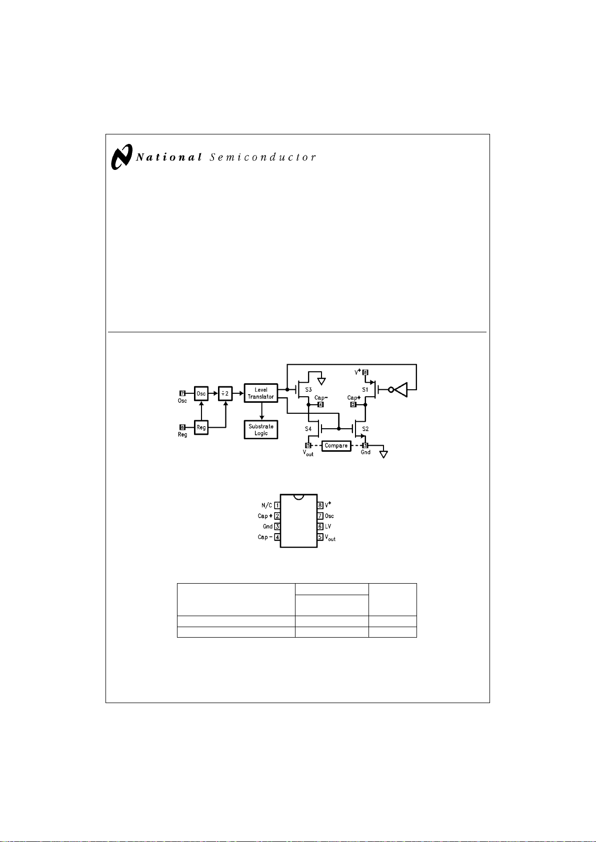
The LMC7660 uses its built-in oscillator to switch 4 power
MOS switches and charge two inexpensive electrolytic capacitors.
Features
n Operation over full temperature and voltage range
without an external diode
n Low supply current, 200 µA max
n Pin-for-pin replacement for the 7660
n Wide operating range 1.5V to 10V
n 97%Voltage Conversion Efficiency
n 95%Power Conversion Efficiency
n Easy to use, only 2 external components
n Extended temperature range
n Narrow SO-8 Package
Block Diagram
Pin Configuration
Ordering Information
Package Temperature Range NSC
Drawing
Industrial
−40˚C to +85˚C
8-Lead Molded DIP LMC7660IN N08E
8-Lead Molded Small Outline LMC7660IM M08A
DS009136-1
DS009136-2
April 1997
LMC7660 Switched Capacitor Voltage Converter
© 1997National Semiconductor Corporation DS009136 www.national.com
Absolute Maximum Ratings (Note 1)
If Military/Aerospace specified devices are required,
please contact the National Semiconductor Sales Office/
Distributors for availability and specifications.
Supply Voltage 10.5V
Input Voltage on Pin 6, 7
(Note 2) −0.3V to (V
+
+ 0.3V)
for V
+
<
5.5V
(V
+
− 5.5V) to (V++ 0.3V)
for V
+
>
5.5V
Current into Pin 6 (Note 2) 20 µA
Output Short Circuit
Duration (V
+
≤ 5.5V) Continuous
Power Dissipation (Note 3)
Dual-In-Line Package 1.4W
Surface-Mount Package 0.6W
T
J
Max (Note 3) 150˚C
θ
JA
(Note 3)
Dual-In-Line Package 90˚C/W
Surface-Mount Package 160˚C/W
Storage Temp. Range −65˚C ≤ T ≤ 150˚C
Lead Temperature
(Soldering, 5 sec.) 260˚C
ESD Tolerance (Note 7)
±
2000V
Electrical Characteristics (Note 4)
Symbol Parameter Conditions Typ
LMC7660IN/
Units
Limits
LMC7660IM
Limit
(Note 5)
I
s
Supply Current R
L
=
∞
120 200 µA
400 max
V
+
H Supply Voltage R
L
=
10 kΩ, Pin 6 Open 3 to 10 3 to 10 V
Range High (Note 6) Voltage Efficiency ≥ 90
%
3to10
V
+
L Supply Voltage R
L
=
10 kΩ, Pin 6 to Gnd. 1.5 to 3.5 1.5 to 3.5 V
Range Low Voltage Efficiency ≥ 90
%
1.5 to 3.5
R
out
Output Source I
L
=
20 mA 55 100 Ω
Resistance 120 max
V=2V, I
L
=
3 mA 110 200 Ω
Pin 6 Short to Gnd. 300 max
F
osc
Oscillator 10 kHz
Frequency
P
eff
Power Efficiency R
L
=
5kΩ 97 95
%
90 min
V
o eff
Voltage Conversion R
L
=
∞
99.9 97
%
Efficiency 95 min
I
osc
Oscillator Sink or Pin 7=Gnd. or V
+
3µA
Source Current
Note 1: Absolute Maximum ratings indicate limits beyond which damage to the device may occur. DC and AC electrical specifications do not apply when operating
the device beyond its rated operating conditions. See Note 4 for conditions.
Note 2: Connecting any input terminal to voltages greater than V
+
or less than ground may cause destructive latchup. It is recommended that no inputs from sources
operating from external supplies be applied prior to “power-up” of the LMC7660.
Note 3: For operation at elevated temperature, these devices must be derated based on a thermal resistance of θ
ja
and Tjmax, T
j
=
T
A
+ θjaPD.
Note 4: Boldface numbers apply at temperature extremes. All other numbers apply at T
A
=
25˚C, V
+
=
5V, C
osc
=
0, and apply for the LMC7660 unless otherwise
specified. Test circuit is shown in
Figure 1
.
Note 5: Limits at room temperature are guaranteed and 100%production tested. Limits in boldface are guaranteed over the operating temperature range (but not
100%tested), and are not used to calculate outgoing quality levels.
Note 6: The LMC7660 can operate without an external diode over the full temperature and voltage range. The LMC7660 can also be used with the external diode
Dx, when replacing previous 7660 designs.
Note 7: The test circuit consists of the human body model of 100 pF in series with 1500Ω.
www.national.com 2
Electrical Characteristics (Note 4) (Continued)
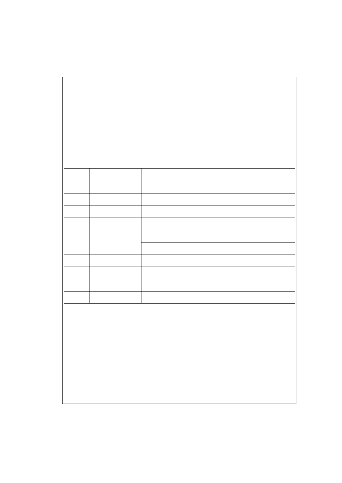
Typical Performance Characteristics
DS009136-5
FIGURE 1. LMC7660 Test Circuit
OSC Freq. vs OSC
Capacitance
DS009136-18
V
out
vs I
out
@
V
+
=
2V
DS009136-19
V
out
vs I
out
@
V
+
=
5V
DS009136-20
Supply Current & Power Efficiency
vs Load Current (V
+
=
2V)
DS009136-21
Supply Current & Power Efficiency
vs Load Current (V
+
=
5V)
DS009136-22
Output Source Resistiance as a
Function of Temperature
DS009136-23
3 www.national.com
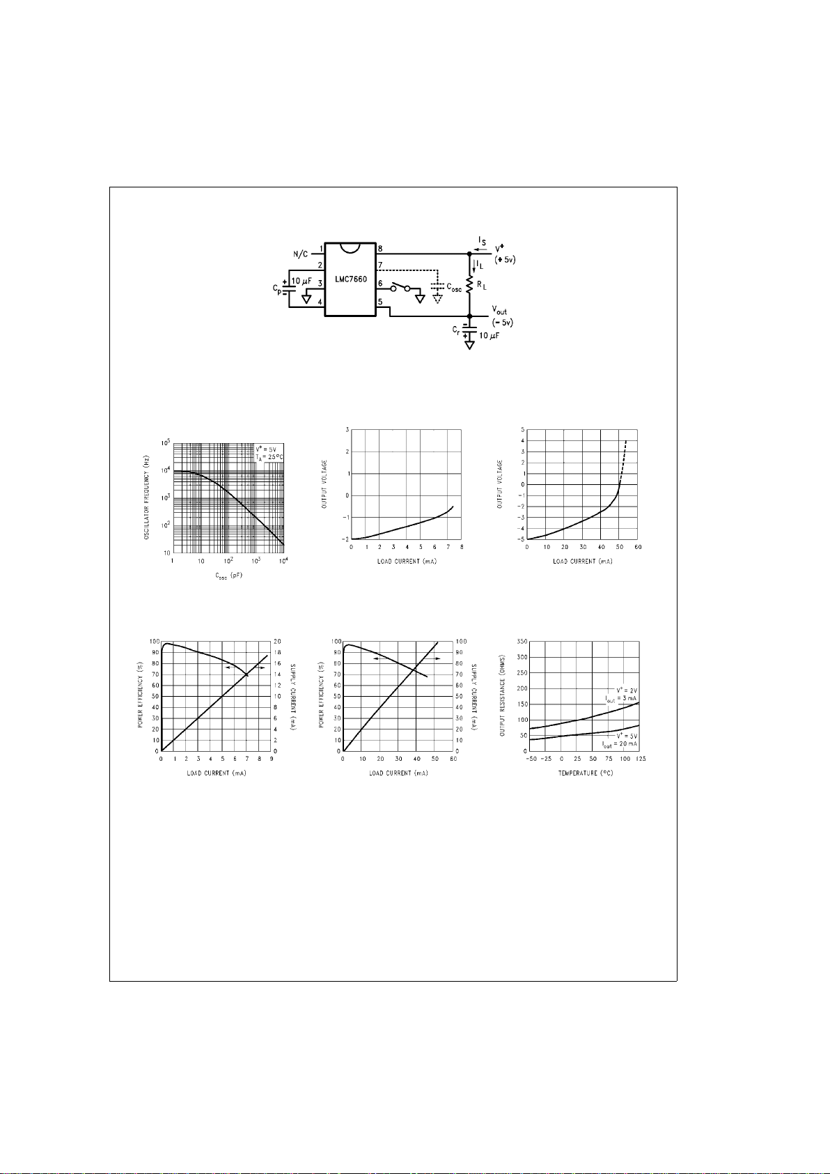
Typical Performance Characteristics (Continued)
Application Information
Circuit Description
The LMC7660 contains four large CMOS switches which are
switched in a sequence to provide supply inversion V
out
=
−V
in
. Energy transfer and storage are provided by two inex-
pensive electrolytic capacitors.
Figure 2
shows how the
LMC7660 can be used to generate −V
+
from V+. When
switches S1 and S3 are closed, C
p
charges to the supply
voltage V
+
. During this time interval, switches S2 and S4 are
open.After C
p
charges to V+, S1 and S3 are opened, S2 and
S4 are then closed. By connecting S2 to ground, C
p
devel-
ops a voltage −V
+
/2 on Cr.After a number of cycles Crwill be
pumped to exactly −V
+
. This transfer will be exact assuming
no load on C
r
, and no loss in the switches.
In the circuit of
Figure 2
, S1 is a P-channel device and S2,
S3, and S4 are N-channel devices. Because the output is biased below ground, it is important that the p
−
wells of S3 and
S4 never become forward biased with respect to either their
sources or drains. A substrate logic circuit guarantees that
these p
−
wells are always held at the proper voltage. Under
all conditions S4 p
−
well must be at the lowest potential in the
circuit. To switch off S4, a level translator generates V
GS4
=
0V, and this is accomplished by biasing the level translator
from the S4 p
−
well.
An internal RC oscillator and
÷
2 circuit provide timing signals to the level translator. The built-in regulator biases the
oscillator and divider to reduce power dissipation on high
supply voltage. The regulator becomes active at about V
+
=
6.5V.Low voltage operation can be improved if the LV pin is
shorted to ground for V
+
≤ 3.5V. For V+≥ 3.5V, the LV pin
must be left open to prevent damage to the part.
Power Efficiency and Ripple
It is theoretically possible to approach 100%efficiency if the
following conditions are met:
1. The drive circuitry consumes little power.
2. The power switches are matched and have low R
on
.
3. The impedance of the reservoir and pump capacitors are
negligibly small at the pumping frequency.
The LMC7660 closely approaches 1 and 2 above. By using
a large pump capacitor C
p
, the charge removed while sup-
plying the reservoir capacitor is small compared to C
p
’s total
charge. Small removed charge means small changes in the
pump capacitor voltage, and thus small energy loss and high
efficiency. The energy loss by C
p
is:
By using a large reservoir capacitor, the output ripple can be
reduced to an acceptable level. For example, if the load current is 5 mA and the accepted ripple is 200 mV,then the reservoir capacitor can omit approximately be calculated from:
Precautions
1. Do not exceed the maximum supply voltage or junction
temperature.
2. Do not short pin 6 (LV terminal) to ground for supply volt-
ages greater than 3.5V.
3. Do not short circuit the output to V
+
.
4. External electrolytic capacitors C
r
and Cpshould have
their polarities connected as shown in
Figure 1
.
Replacing Previous 7660 Designs
To prevent destructive latchup, previous 7660 designs require a diode in series with the output when operated at elevated temperature or supply voltage. Although this prevented the latchup problem of these designs, it lowered the
available output voltage and increased the output series resistance.
The National LMC7660 has been designed to solve the inherent latch problem. The LCM7660 can operate over the
entire supply voltage and temperature range without the
need for an output diode. When replacing existing designs,
the LMC7660 can be operated with diode Dx.
Unloaded Oscillator Frequency
as a Function of Temperature
DS009136-24
Output R vs Supply Voltage
DS009136-25
P
eff
vs OSC Freq.@V
+
=
5V
DS009136-26
www.national.com 4

Application Information (Continued)
Typical Applications
Changing Oscillator Frequency
It is possible to dramatically reduce the quiescent operating
current of the LMC7660 by lowering the oscillator frequency.
The oscillator frequency can be lowered from a nominal 10
kHz to several hundred hertz, by adding a slow-down capacitor C
osc
(
Figure 3
).As shown in theTypical Performance
Curves the supply current can be lowered to the 10 µA
range. This low current drain can be extremely useful when
used in µPower and battery back-up equipment. It must be
understood that the lower operating frequency and supply
current cause an increased impedance of C
r
and Cp. The increased impedance, due to a lower switching rate, can be
offset by raising C
r
and Cpuntil ripple and load current re-
quirements are met.
Synchronizing to an External Clock
Figure 4
shows an LMC7660 synchronized to an external
clock. The CMOS gate overrides the internal oscillator when
it is necessary to switch faster or reduce power supply interference. The external clock still passes through the
÷
2 circuit
in the 7660, so the pumping frequency will be
1
⁄2the external
clock frequency.
Lowering Output Impedance
Paralleling two or more LMC7660’s lowers output impedance. Each device must have it’s own pumping capacitor C
p
,
but the reservoir capacitor C
r
is shared as depicted in
Figure
5
. The composite output resistance is:
DS009136-6
FIGURE 2. Idealized Voltage Converter
DS009136-7
FIGURE 3. Reduce Supply Current by Lowering Oscillator Frequency
DS009136-8
FIGURE 4. Synchronizing to an External Clock
5 www.national.com

Typical Applications (Continued)
Increasing Output Voltage
Stacking the LMC7660s is an easy way to produce a greater
negative voltage. It should be noted that the input current required for each stage is twice the load current on that stage
as shown in
Figure 6
. The effective output resistance is ap-
proximately the sum of the individual R
out
values, and so
only a few levels of multiplication can be used.
It is possible to generate −15V from +5V by connecting the
second 7660’s pin 8 to +5V instead of ground as shown in
Figure 7
. Note that the second 7660 sees a full 20V and the
input supply should not be increased beyond +5V.
Split V
+
In Half
Figure 8
is one of the more interesting applications for the
LMC7660. The circuit can be used as a precision voltage divider (for very light loads), alternately it is used to generate a
1
⁄2supply point in battery applications. In the1⁄2cycle when
S1 and S3 are closed, the supply voltage divides across the
capacitors in a conventional way proportional to their value.
In the
1
⁄2cycle when S2 and S4 are closed, the capacitors
switch from a series connection to a parallel connection. This
forces the capacitors to have the same voltage; the charge
redistributes to maintain precisely V
+
/2, across Cpand Cr.In
this application all devices are only V
+
/2, and the supply volt-
age can be raised to 20V giving exactly 10V at V
out
.
DS009136-9
FIGURE 5. Lowering Output Resistance by Paralleling Devices
DS009136-10
FIGURE 6. Higher Voltage by Cascade
DS009136-11
FIGURE 7. Getting −15V from +5V
www.national.com 6

Typical Applications (Continued)
Getting Up … and Down
The LMC7660 can also be used as a positive voltage multiplier. This application, shown in
Figure 9
, requires 2 addi-
tional diodes. During the first
1
⁄2cycle S2 charges Cp1
through D1; D2 is reverse biased. In the next
1
⁄2cycle S2 is
open and S1 is closed. Since C
p
1 is charged to V+−VD1and
is referenced to V
+
through S1, the junction of D1 and D2 is
at V
+
+(V+−VD1). D1 is reverse biased in this interval. This
application uses only two of the four switches in the 7660.
The other two switches can be put to use in performing a
negative conversion at the same time as shown in
Figure 10
.
In the
1
⁄2cycle that D1 is charging Cp1, Cp2 is connected
from ground to −V
out
via S2 and S4, and Cr2 is storing Cp2’s
charge. In the interval that S1 and S3 are closed, C
p
1 pumps
the junction of D1 and D2 above V
+
, while Cp2 is refreshed
from V
+
.
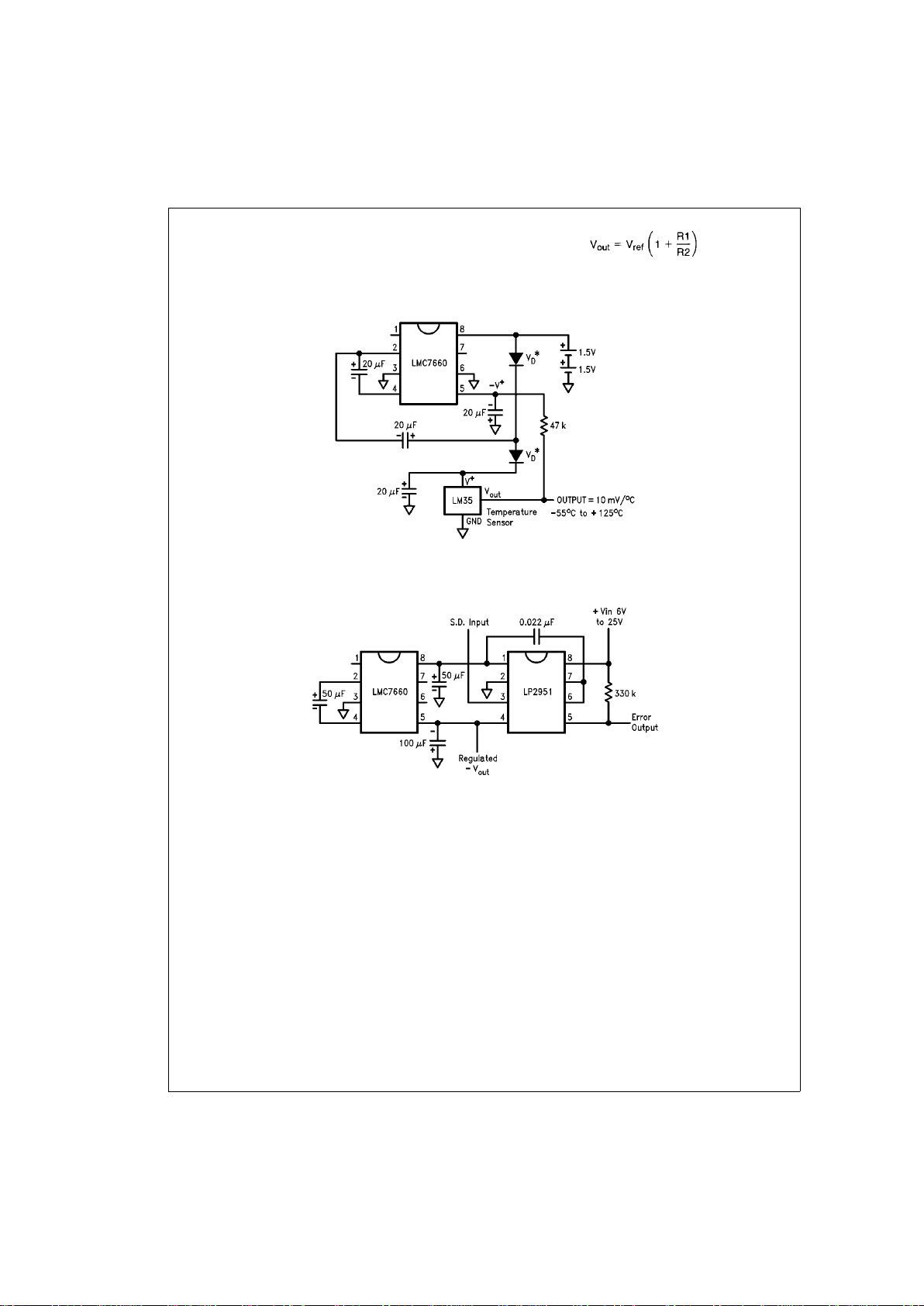
Thermometer Spans 180˚C
Using the combined negative and positive multiplier of
Fig-
ure 11
with an LM35 it is possible to make a µPower thermometer that spans a 180˚C temperature range. The LM35
temperature sensor has an output sensitivity of 10 mV/˚C,
while drawing only 50 µA of quiescent current. In order for
the LM35 to measure negative temperatures, a pull down to
a negative voltage is required.
Figure 11
shows a thermometer circuit for measuring temperatures from −55˚C to
+125˚C and requiring only two 1.5V cells. End of battery life
can be extended by replacing the up converter diodes with
Schottky’s.
Regulating −V
out
It is possible to regulate the output of the LMC7660 and still
maintain µPower performance. This is done by enclosing the
LMC7660 in a loop with a LP2951. The circuit of
Figure 12
will regulate V
out
to −5V for I
L
=
10 mA, and V
in
=
6V.For V
in
>
7V,the output stays in regulation up to I
L
=
25 mA.The error flag on pin 5 of the LP2951 sets low when the regulated
output at pin 4 drops by about 5%. The LP2951 can be shutdown by taking pin 3 high; the LMC7660 can be shutdown by
shorting pin 7 and pin 8.
DS009136-12
FIGURE 8. Split V+in Half
DS009136-13
FIGURE 9. Positive Voltage Multiplier
DS009136-14
FIGURE 10. Combined Negative Converter and Positive Multiplier
7 www.national.com
Typical Applications (Continued)
The LP2951 can be reconfigured to an adjustable type regulator,which means the LMC7660 can give a regulated output
from −2.0V to −10V dependent on the resistor ratios R1 and
R2, as shown in
Figure 13
,V
ref
=
1.235V:
DS009136-15
*
For lower voltage operation, use Schottky rectifiers
FIGURE 11. µPower Thermometer Spans 180˚C, and Pulls Only 150 µA
DS009136-16
FIGURE 12. Regulated −5V with 200 µA Standby Current
www.national.com 8

Typical Applications (Continued)
DS009136-17
V
ref
=
1.235V
*
Low voltage operation
FIGURE 13. LMC7660 and LP2951 Make a Negative Adjustable Regulator
9 www.national.com

10

Physical Dimensions inches (millimeters)
Molded Small Outline Package (M)
Order Number LMC7660IM
NS Package Number M08A
Molded Dual-In-Line Package (N)
Order Number LMC7660IN
NS Package Number N08E
11 www.national.com

LIFE SUPPORT POLICY
NATIONAL’S PRODUCTS ARE NOT AUTHORIZED FOR USE AS CRITICAL COMPONENTS IN LIFE SUPPORT DEVICES OR SYSTEMS WITHOUT THE EXPRESS WRITTEN APPROVAL OF THE PRESIDENT OF NATIONAL SEMICONDUCTOR CORPORATION. As used herein:
1. Life support devices or systems are devices or systems which, (a) are intended for surgical implant into
the body,or (b) support orsustain life, and whosefailure to perform when properly used in accordance
with instructions for use provided in the labeling, can
be reasonablyexpected to result in a significant injury
to the user.
2. A critical component in any component of a life support
device or system whose failure to perform can be reasonably expected to cause the failure of the life support
device orsystem, or to affect its safety or effectiveness.
National Semiconductor
Corporation
1111 West Bardin Road
Arlington, TX 76017
Tel: 1(800) 272-9959
Fax: 1(800) 737-7018
www.national.com
National Semiconductor
Europe
Fax: (+49) 0-180-530 85 86
Email: cnjwge@tevm2.nsc.com
Deutsch Tel: (+49) 0-180-530 85 85
English Tel: (+49) 0-180-532 78 32
Français Tel: (+49) 0-180-532 93 58
Italiano Tel: (+49) 0-180-534 16 80
National Semiconductor
Hong Kong Ltd.
13th Floor, Straight Block,
Ocean Centre, 5 Canton Rd.
Tsimshatsui, Kowloon
Hong Kong
Tel: (852) 2737-1600
Fax: (852) 2736-9960
National Semiconductor
Japan Ltd.
Tel: 81-043-299-2308
Fax: 81-043-299-2408
LMC7660 Switched Capacitor Voltage Converter
National does not assume any responsibility for use of any circuitry described, no circuit patent licenses are implied and National reserves the right at any time without notice to change said circuitry and specifications.
 Loading...