

LMC6462 Dual/LMC6464 Quad
Micropower, Rail-to-Rail Input and Output CMOS
Operational Amplifier
General Description
The LMC6462/4 is a micropower version of the popular
LMC6482/4, combining Rail-to-Rail Input and Output Range
with very low power consumption.
The LMC6462/4 provides an input common-mode voltage
range that exceeds both rails.The rail-to-rail output swing of
the amplifier, guaranteed for loads down to 25 kΩ, assures
maximum dynamic sigal range. This rail-to-rail performance
of the amplifier, combined with its high voltage gain makes it
unique among rail-to-rail amplifiers. The LMC6462/4 is an
excellent upgrade for circuits using limited common-mode
range amplifiers.
The LMC6462/4, with guaranteed specifications at 3V and
5V, is especially well-suited for low voltage applications. A
quiescent power consumption of 60 µW per amplifier (at V
S
=
3V) can extend the useful life of battery operated systems.
The amplifier’s 150 fA input current, low offset voltage of
0.25 mV, and 85 dB CMRR maintain accuracy in
battery-powered systems.
Features
(Typical unless otherwise noted)
n Ultra Low Supply Current 20 µA/Amplifier
n Guaranteed Characteristics at 3V and 5V
n Rail-to-Rail Input Common-Mode Voltage Range
n Rail-to-Rail Output Swing
(within 10 mV of rail, V
S
=
5V and R
L
=
25 kΩ)
n Low Input Current 150 fA
n Low Input Offset Voltage 0.25 mV
Applications
n Battery Operated Circuits
n Transducer Interface Circuits
n Portable Communication Devices
n Medical Applications
n Battery Monitoring
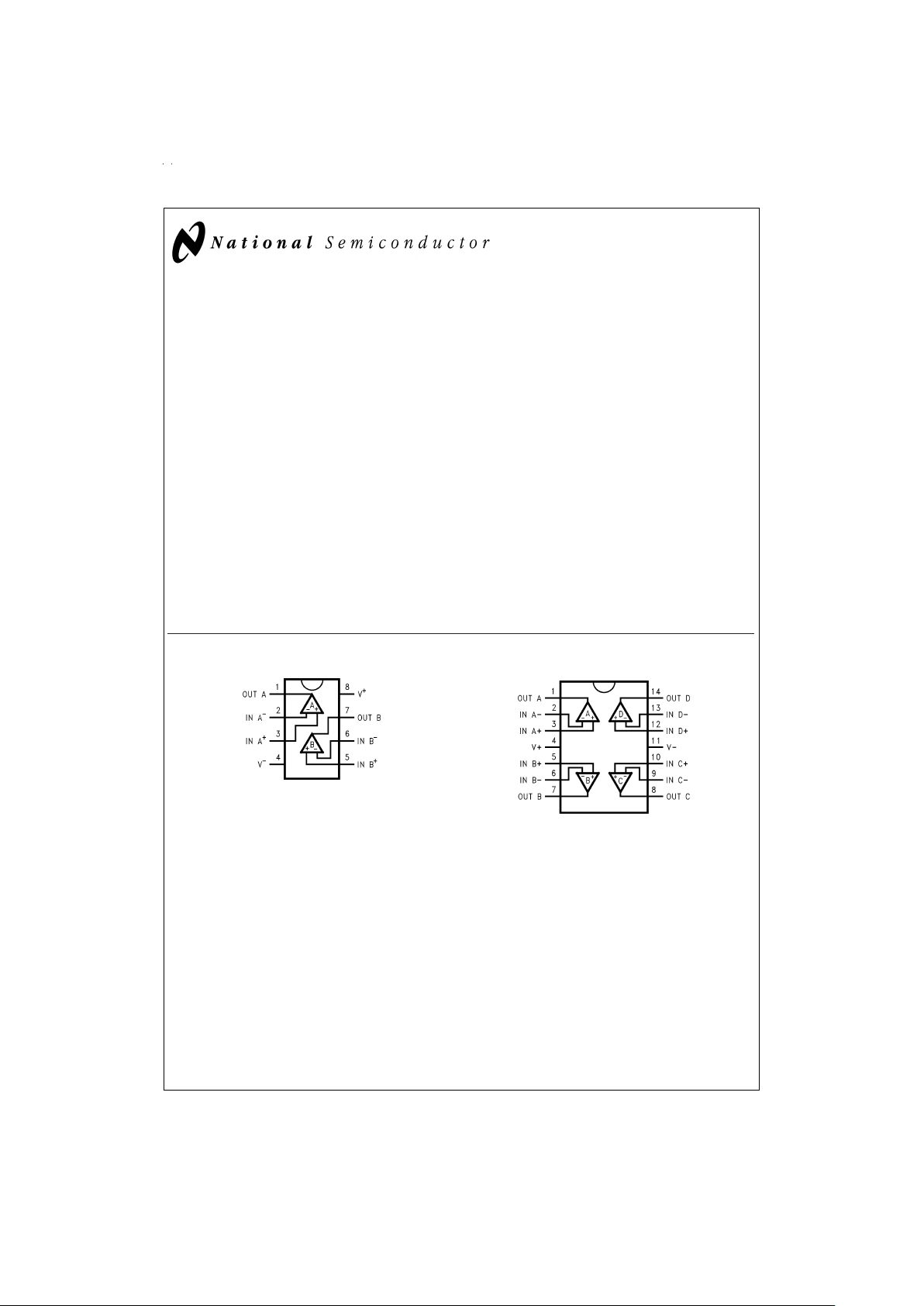
8-Pin DIP/SO
DS012051-1
Top View
14-Pin DIP/SO
DS012051-2
Top View
May 1999
LMC6462 Dual/LMC6464 Quad Micropower, Rail-to-Rail Input and Output CMOS Operational
Amplifier
© 1999 National Semiconductor Corporation DS012051 www.national.com
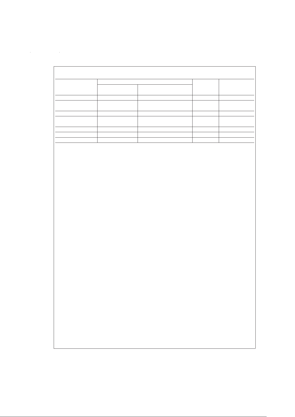
Ordering Information
Package Temperature Range NSC Transport
Military Industrial Drawing Media
−55˚C to +125˚C −40˚C to +85˚C
8-Pin Molded DIP LMC6462AMN LMC6462AIN, LMC6462BIN N08E Rails
8-Pin SO-8 LMC6462AIM, LMC6462BIM M08A Rails
LMC6462AIMX, LMC6462BIMX M08A Tape and Reel
14-Pin Molded DIP LMC6464AMN LMC6464AIN, LMC6464BIN N14A Rails
14-Pin SO-14 LMC6464AIM, LMC6464BIM M14A Rails
LMC6464AIMX, LMC6464BIMX M14A Tape and Reel
8-Pin Ceramic DIP LMC6462AMJ-QML J08A Rails
14-Pin Ceramic DIP LMC6464AMJ-QML J14A Rails
14-Pin Ceramic SOIC LMC6464AMWG-QML WG14A Trays
www.national.com 2
Absolute Maximum Ratings (Note 1)
If Military/Aerospace specified devices are required,
please contact the National Semiconductor Sales Office/
Distributors for availability and specifications.
ESD Tolerance (Note 2) 2.0 kV
Differential Input Voltage
±
Supply Voltage
Voltage at Input/Output Pin (V
+
) + 0.3V, (V−) − 0.3V
Supply Voltage (V
+−V−
) 16V
Current at Input Pin (Note 12)
±
5mA
Current at Output Pin
(Notes 3, 8)
±
30 mA
Current at Power Supply Pin 40 mA
Lead Temp. (Soldering, 10 sec.) 260˚C
Storage Temperature Range −65˚C to +150˚C
Junction Temperature (Note 4) 150˚C
Operating Ratings (Note 1)
Supply Voltage 3.0V ≤ V
+
≤ 15.5V
Junction Temperature Range
LMC6462AM, LMC6464AM −55˚C ≤ T
J
≤ +125˚C
LMC6462AI, LMC6464AI −40˚C ≤ T
J
≤ +85˚C
LMC6462BI, LMC6464BI −40˚C ≤ T
J
≤ +85˚C
Thermal Resistance (θ
JA
)
N Package, 8-Pin Molded DIP 115˚C/W
M Package, 8-Pin Surface Mount 193˚C/W
N Package, 14-Pin Molded DIP 81˚C/W
M Package, 14-Pin
Surface Mount 126˚C/W
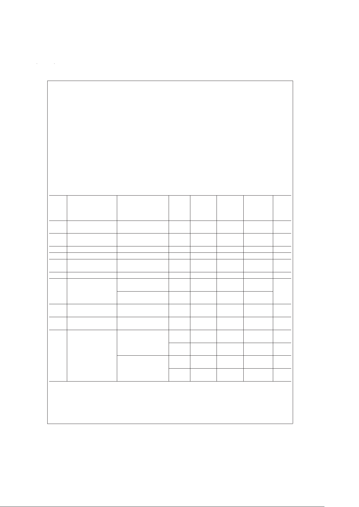
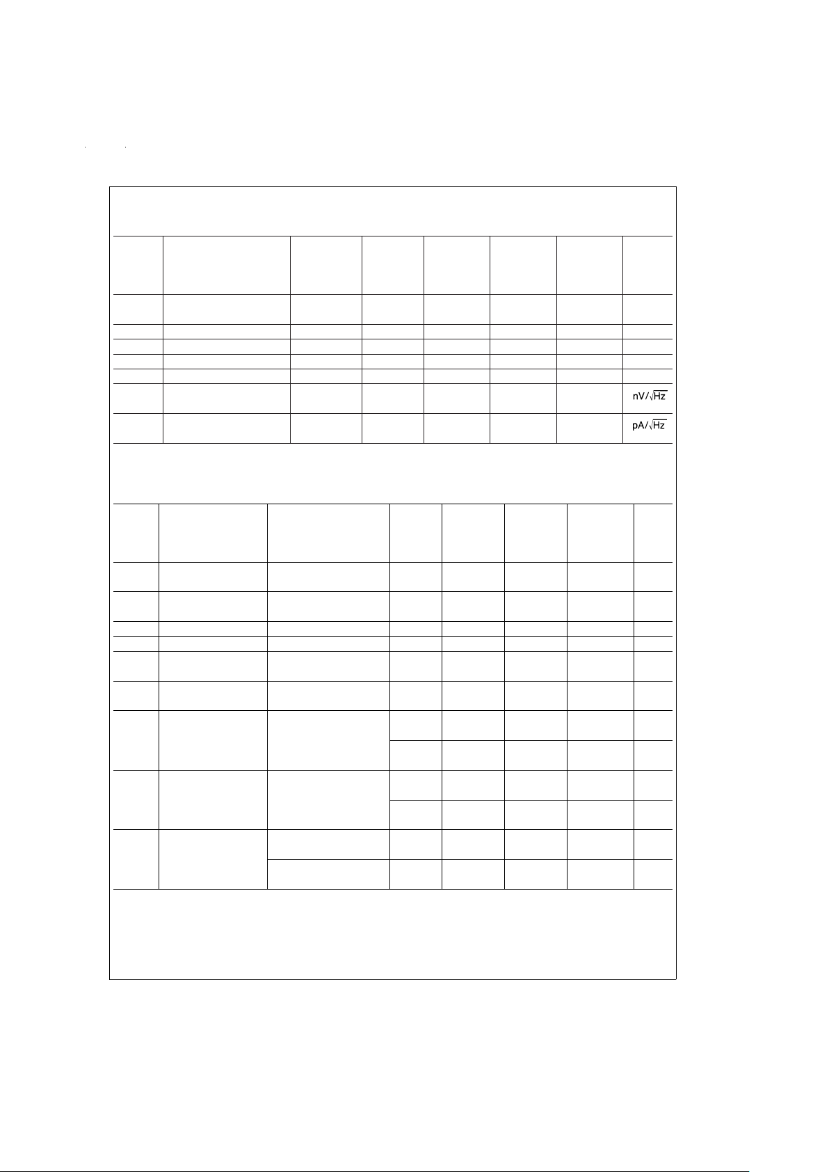
5V DC Electrical Characteristics
Unless otherwise specified, all limits guaranteed for T
J
=
25˚C, V
+
=
5V, V
−
=
0V, V
CM
=
V
O
=
V
+
/2 and R
L
>
1M. Boldface
limits apply at the temperature extremes.
LMC6462AI LMC6462BI LMC6462AM
Symbol Parameter Conditions Typ LMC6464AI LMC6464BI LMC6464AM Units
(Note 5) Limit Limit Limit
(Note 6) (Note 6) (Note 6)
V
OS
Input Offset Voltage 0.25 0.5 3.0 0.5 mV
1.2 3.7 1.5 max
TCV
OS
Input Offset Voltage 1.5 µV/˚C
Average Drift
I
B
Input Current (Note 13) 0.15 10 10 200 pA max
I
OS
Input Offset Current (Note 13) 0.075 5 5 100 pA max
C
IN
Common-Mode 3 pF
Input Capacitance
R
IN
Input Resistance
>
10 Tera Ω
CMRR Common Mode 0V ≤ V
CM
≤ 15.0V, 85 70 65 70 dB
min
Rejection Ratio V
+
=
15V 67 62 65
0V ≤ V
CM
≤ 5.0V 85 70 65 70
V
+
=
5V 67 62 65
+PSRR Positive Power Supply 5V ≤ V
+
≤ 15V, 85 70 65 70 dB
Rejection Ratio V
−
=
0V, V
O
=
2.5V 67 62 65 min
−PSRR Negative Power Supply −5V ≤ V
−
≤ −15V, 85 70 65 70 dB
Rejection Ratio V
+
=
0V, V
O
=
−2.5V 67 62 65 min
V
CM
Input Common-Mode V
+
=
5V −0.2 −0.10 −0.10 −0.10 V
Voltage Range For CMRR ≥ 50 dB 0.00 0.00 0.00 max
5.30 5.25 5.25 5.25 V
5.00 5.00 5.00 min
V
+
=
15V −0.2 −0.15 −0.15 −0.15 V
For CMRR ≥ 50 dB 0.00 0.00 0.00 max
15.30 15.25 15.25 15.25 V
15.00 15.00 15.00 min
www.national.com3
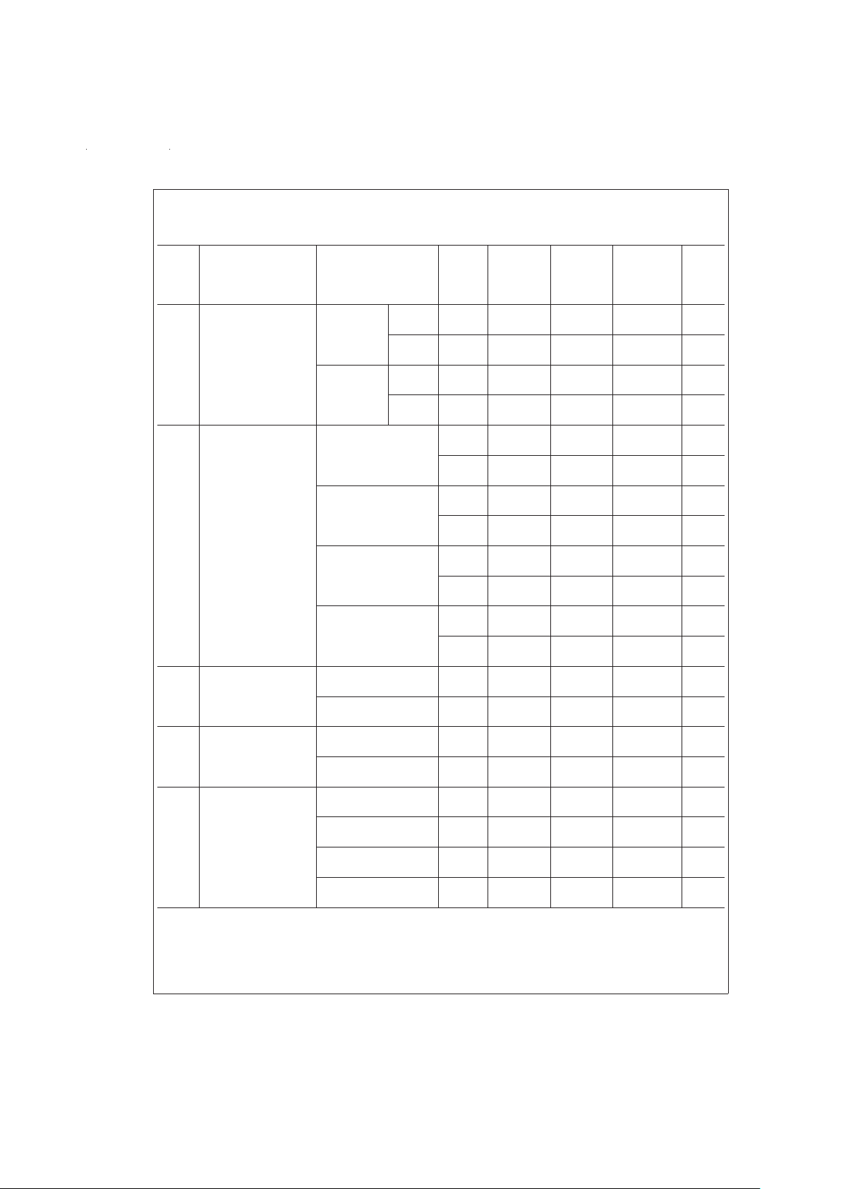
5V DC Electrical Characteristics (Continued)
Unless otherwise specified, all limits guaranteed for T
J
=
25˚C, V
+
=
5V, V
−
=
0V, V
CM
=
V
O
=
V
+
/2 and R
L
>
1M. Boldface
limits apply at the temperature extremes.
LMC6462AI LMC6462BI LMC6462AM
Symbol Parameter Conditions Typ LMC6464AI LMC6464BI LMC6464AM Units
(Note 5) Limit Limit Limit
(Note 6) (Note 6) (Note 6)
A
V
Large Signal R
L
=
100 kΩ Sourcing 3000 V/mV
Voltage Gain (Note 7) min
Sinking 400 V/mV
min
R
L
=
25 kΩ Sourcing 2500 V/mV
(Note 7) min
Sinking 200 V/mV
min
V
O
Output Swing V
+
=
5V 4.995 4.990 4.950 4.990 V
R
L
=
100 kΩ to V
+
/2 4.980 4.925 4.970 min
0.005 0.010 0.050 0.010 V
0.020 0.075 0.030 max
V
+
=
5V 4.990 4.975 4.950 4.975 V
R
L
=
25 kΩ to V
+
/2 4.965 4.850 4.955 min
0.010 0.020 0.050 0.020 V
0.035 0.150 0.045 max
V
+
=
15V 14.990 14.975 14.950 14.975 V
R
L
=
100 kΩ to V
+
/2 14.965 14.925 14.955 min
0.010 0.025 0.050 0.025 V
0.035 0.075 0.050 max
V
+
=
15V 14.965 14.900 14.850 14.900 V
R
L
=
25 kΩ to V
+
/2 14.850 14.800 14.800 min
0.025 0.050 0.100 0.050 V
0.150 0.200 0.200 max
I
SC
Output Short Circuit Sourcing, V
O
=
0V 27 19 19 19 mA
Current 15 15 15 min
V+=5V Sinking, V
O
=
5V 27 22 22 22 mA
17 17 17 min
I
SC
Output Short Circuit Sourcing, V
O
=
0V 38 24 24 24 mA
Current 17 17 17 min
V
+
=
15V Sinking, V
O
=
12V 75 55 55 55 mA
(Note 8) 45 45 45 min
I
S
Supply Current Dual, LMC6462 40 55 55 55 µA
V
+
=
+5V, V
O
=
V
+
/2 70 70 75 max
Quad, LMC6464 80 110 110 110 µA
V
+
=
+5V, V
O
=
V
+
/2 140 140 150 max
Dual, LMC6462 50 60 60 60 µA
V
+
=
+15V, V
O
=
V
+
/2 70 70 75 max
Quad, LMC6464 90 120 120 120 µA
V
+
=
+15V, V
O
=
V
+
/2 140 140 150 max
www.national.com 4
5V AC Electrical Characteristics
Unless otherwise specified, all limits guaranteed for T
J
=
25˚C, V
+
=
5V, V
−
=
0V, V
CM
=
V
O
=
V
+
/2 and R
L
>
1M. Boldface
limits apply at the temperature extremes.
LMC6462AI LMC6462BI LMC6462AM
Symbol Parameter Conditions Typ LMC6464AI LMC6464BI LMC6464AM Units
(Note 5) Limit Limit Limit
(Note 6) (Note 6) (Note 6)
SR Slew Rate (Note 9) 28 15 15 15 V/ms
888min
GBW Gain-Bandwidth Product V
+
=
15V 50 kHz
φ
m
Phase Margin 50 Deg
G
m
Gain Margin 15 dB
Amp-to-Amp Isolation (Note 10) 130 dB
e
n
Input-Referred f=1 kHz 80
Voltage Noise V
CM
=
1V
i
n
Input-Referred f=1 kHz 0.03
Current Noise
3V DC Electrical Characteristics
Unless otherwise specified, all limits guaranteed for T
J
=
25˚C, V
+
=
3V, V
−
=
0V, V
CM
=
V
O
=
V
+
/2 and R
L
>
1M. Boldface
limits apply at the temperature extremes.
LMC6462AI LMC6462BI LMC6462AM
Symbol Parameter Conditions Typ LMC6464AI LMC6464BI LMC6464AM Units
(Note 5) Limit Limit Limit
(Note 6) (Note 6) (Note 6)
V
OS
Input Offset Voltage 0.9 2.0 3.0 2.0 mV
2.7 3.7 3.0 max
TCV
OS
Input Offset Voltage 2.0 µV/˚C
Average Drift
I
B
Input Current (Note 13) 0.15 10 10 200 pA
I
OS
Input Offset Current (Note 13) 0.075 5 5 100 pA
CMRR Common Mode 0V ≤ V
CM
≤ 3V 74 60 60 60 dB
Rejection Ratio min
PSRR Power Supply 3V ≤ V
+
≤ 15V, V
−
=
0V 80 60 60 60 dB
Rejection Ratio min
V
CM
Input Common-Mode For CMRR ≥ 50 dB −0.10 0.0 0.0 0.0 V
Voltage Range max
3.0 3.0 3.0 3.0 V
min
V
O
Output Swing R
L
=
25 kΩ to V
+
/2 2.95 2.9 2.9 2.9 V
min
0.15 0.1 0.1 0.1 V
max
I
S
Supply Current Dual, LMC6462 40 55 55 55 µA
V
O
=
V
+
/2 70 70 70
Quad, LMC6464 80 110 110 110 µA
V
O
=
V
+
/2 140 140 140 max
www.national.com5
3V AC Electrical Characteristics
Unless otherwise specified, V
+
=
3V, V
−
=
0V, V
CM
=
V
O
=
V
+
/2 and R
L
>
1M. Boldface limits apply at the temperature ex-
tremes.
LMC6462AI LMC6462BI LMC6462AM
Symbol Parameter Conditions Typ LMC6464AI LMC6464BI LMC6464AM Units
(Note 5) Limit Limit Limit
(Note 6) (Note 6) (Note 6)
SR Slew Rate (Note 11) 23 V/ms
GBW Gain-Bandwidth Product 50 kHz
Note 1: Absolute Maximum Ratings indicate limits beyond which damage to the device may occur. Operating Ratings indicate conditions for which the device is intended to be functional, but specific performance is not guaranteed. For guaranteed specifications and the test conditions, see the Electrical Characteristics.
Note 2: Human body model, 1.5 kΩ in series with 100 pF. All pins rated per method 3015.6 of MIL-STD-883. This is a class 2 device rating.
Note 3: Applies to both single supply and split-supply operation. Continuous short circuit operationatelevatedambienttemperaturecanresultinexceedingthe maxi-
mum allowed junction temperature of 150˚C. Output currents in excess of
±
30 mA over long term may adversely affect reliability.
Note 4: The maximum power dissipation is a function of T
J(max)
, θJA, and TA. The maximum allowable power dissipation at any ambient temperature is P
D
=
(T
J(max)
−TA)/θJA. All numbers apply for packages soldered directly into a PC board.
Note 5: Typical Values represent the most likely parametric norm.
Note 6: All limits are guaranteed by testing or statistical analysis.
Note 7: V
+
=
15V, V
CM
=
7.5V and R
L
connected to 7.5V. For Sourcing tests, 7.5V ≤ VO≤ 11.5V. For Sinking tests, 3.5V ≤ VO≤ 7.5V.
Note 8: Do not short circuit output to V
+
, when V+is greater than 13V or reliability will be adversely affected.
Note 9: V
+
=
15V. Connected as Voltage Follower with 10V step input. Number specified is the slower of either the positive or negative slew rates.
Note 10: Input referred, V
+
=
15V and R
L
=
100 kΩ connected to 7.5V. Each amp excited in turn with 1 kHz to produce V
O
=
12 V
PP
.
Note 11: Connected as Voltage Follower with 2V step input. Number specified is the slower of either the positive or negative slew rates.
Note 12: Limiting input pin current is only necessary for input voltages that exceed absolute maximum input voltage ratings.
Note 13: Guaranteed limits are dictated by tester limitations and not device performance. Actual performance is reflected in the typical value.
Note 14: For guaranteed Military Temperature Range parameters see RETSMC6462/4X.
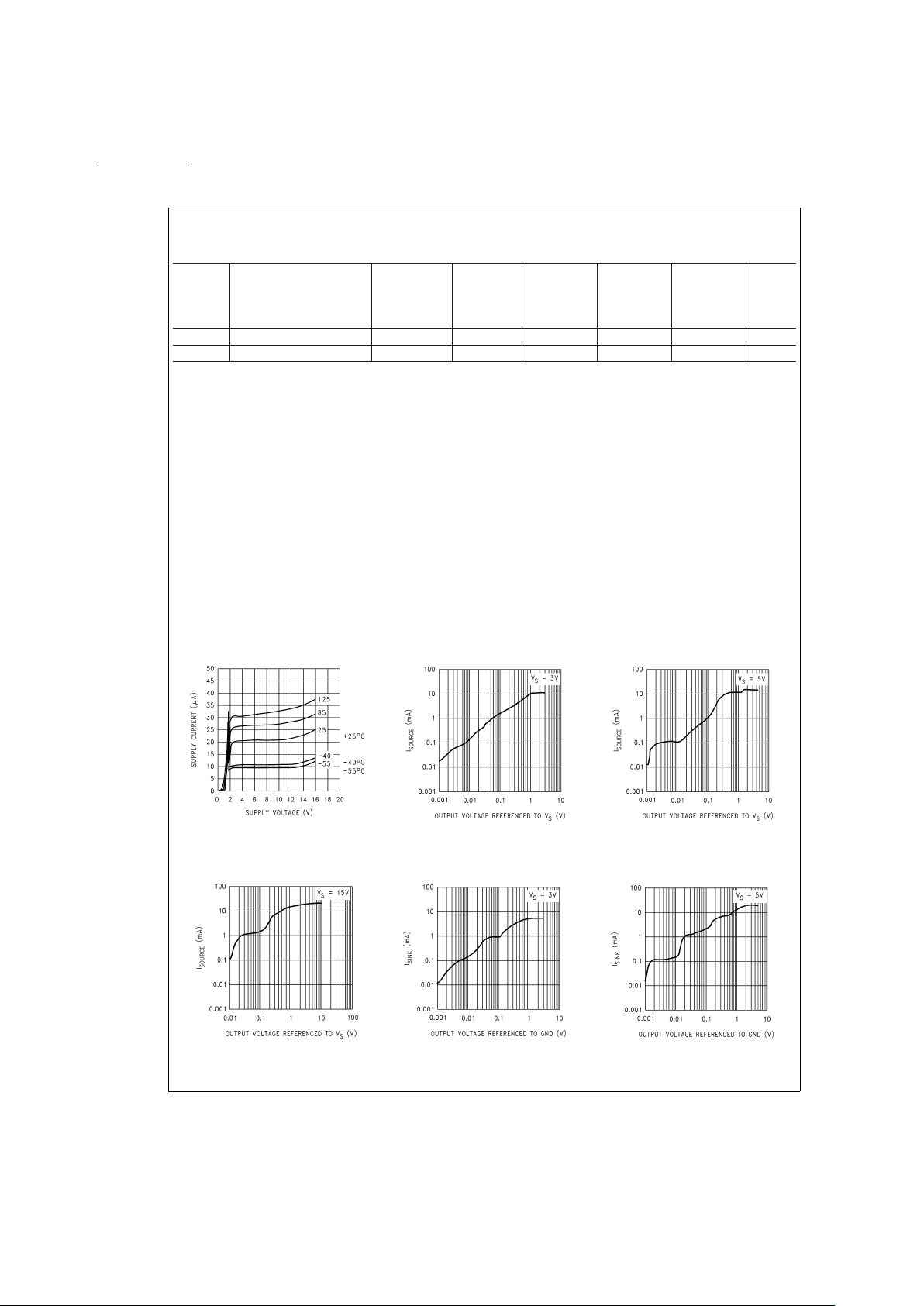
Typical Performance Characteristics V
S
=
+5V, Single Supply, T
A
=
25˚C unless otherwise specified
Supply Current vs
Supply Voltage
DS012051-30
Sourcing Current vs
Output Voltage
DS012051-31
Sourcing Current vs
Output Voltage
DS012051-32
Sourcing Current vs
Output Voltage
DS012051-33
Sinking Current vs
Output Voltage
DS012051-34
Sinking Current vs
Output Voltage
DS012051-35
www.national.com 6

Typical Performance Characteristics V
S
=
+5V, Single Supply, T
A
=
25˚C unless otherwise
specified (Continued)
Sinking Current vs
Output Voltage
DS012051-36
Input Voltage
Noise vs Frequency
DS012051-37
Input Voltage Noise
vs Input Voltage
DS012051-38
Input Voltage Noise
vs Input Voltage
DS012051-39
Input Voltage Noise
vs Input Voltage
DS012051-40
∆VOSvs CMR
DS012051-41
Input Voltage vs
Output Voltage
DS012051-42
Open Loop
Frequency Response
DS012051-43
Open Loop Frequency
Response vs Temperature
DS012051-44
www.national.com7

Typical Performance Characteristics V
S
=
+5V, Single Supply, T
A
=
25˚C unless otherwise
specified (Continued)
Gain and Phase vs
Capacitive Load
DS012051-45
Slew Rate vs
Supply Voltage
DS012051-46
Non-Inverting Large
Signal Pulse Response
DS012051-47
Non-Inverting Large
Signal Pulse Response
DS012051-48
Non-Inverting Large
Signal Pulse Response
DS012051-49
Non-Inverting Small
Signal Pulse Response
DS012051-50
Non-Inverting Small
Signal Pulse Response
DS012051-51
Non-Inverting Small
Signal Pulse Response
DS012051-52
Inverting Large
Signal Pulse Response
DS012051-53
www.national.com 8

Typical Performance Characteristics V
S
=
+5V, Single Supply, T
A
=
25˚C unless otherwise
specified (Continued)
Application Information
1.0 Input Common-Mode Voltage Range
The LMC6462/4 has a rail-to-rail input common-mode voltage range.
Figure 1
shows an input voltage exceeding both
supplies with no resulting phase inversion on the output.
The absolute maximum input voltage at V
+
=
3V is 300 mV
beyond either supply rail at room temperature. Voltages
greatly exceeding this absolute maximum rating, as in
Figure
2
, can cause excessive current to flow in or out of the input
pins, possibly affecting reliability. The input current can be
externally limited to
±
5 mA, with an input resistor, as shown
in
Figure 3
.
Inverting Large Signal
Pulse Response
DS012051-54
Inverting Large Signal
Pulse Response
DS012051-55
Inverting Small Signal
Pulse Response
DS012051-56
Inverting Small Signal
Pulse Response
DS012051-57
Inverting Small Signal
Pulse Response
DS012051-58
DS012051-5
FIGURE 1. An Input Voltage Signal Exceeds
the LMC6462/4 Power Supply Voltage
with No Output Phase Inversion
DS012051-6
FIGURE 2. A±7.5V Input Signal Greatly Exceeds
the 3V Supply in
Figure 3
Causing
No Phase Inversion Due to R
I
www.national.com9

Application Information (Continued)
2.0 Rail-to-Rail Output
The approximated output resistance of the LMC6462/4 is
180Ω sourcing, and 130Ω sinking at V
S
=
3V, and 110Ω
sourcing and 83Ω sinking at V
S
=
5V.The maximum output
swing can be estimated as a function of load using the calculated output resistance.
3.0 Capacitive Load Tolerance
The LMC6462/4 can typically drive a 200 pF load with V
S
=
5V at unity gain without oscillating. The unity gain follower is
the most sensitive configuration to capacitive load. Direct capacitive loading reduces the phase margin of op-amps. The
combination of the op-amp’s output impedance and the capacitive load induces phase lag. This results in either an underdamped pulse response or oscillation.
Capacitive load compensation can be accomplished using
resistive isolation as shown in
Figure 4
. If there is a resistive
component of the load in parallel to the capacitive component, the isolation resistor and the resistive load create a
voltage divider at the output. This introduces a DC error at
the output.
Figure 5
displays the pulse response of the LMC6462/4 cir-
cuit in
Figure 4
.
Another circuit, shown in
Figure 6
, is also used to indirectly
drive capacitive loads. This circuit is an improvement to the
circuit shown in
Figure 4
because it provides DC accuracy as
well as AC stability. R1 and C1 serve to counteract the loss
of phase margin by feeding the high frequency component of
the output signal back to the amplifiers inverting input,
thereby preserving phase margin in the overall feedback
loop. The values of R1 and C1 should be experimentally determined by the system designer for the desired pulse response. Increased capacitive drive is possible by increasing
the value of the capacitor in the feedback loop.
The pulse response of the circuit shown in
Figure 6
is shown
in
Figure 7
.
4.0 Compensating for Input Capacitance
It is quite common to use large values of feedback resistance with amplifiers that have ultra-low input current, like
the LMC6462/4. Large feedback resistors can react with
small values of input capacitance due to transducers, photodiodes, and circuits board parasitics to reduce phase
margins.
DS012051-7
FIGURE 3. Input Current Protection for Voltages
Exceeding the Supply Voltage
DS012051-8
FIGURE 4. Resistive Isolation of
a 300 pF Capacitive Load
DS012051-9
FIGURE 5. Pulse Response of the LMC6462
Circuit Shown in
Figure 4
DS012051-10
FIGURE 6. LMC6462 Non-Inverting Amplifier,
Compensated to Handle a 300 pF Capacitive
and 100 kΩ Resistive Load
DS012051-11
FIGURE 7. Pulse Response of
LMC6462 Circuit in
Figure 6
www.national.com 10

Application Information (Continued)
The effect of input capacitance can be compensated for by
adding a feedback capacitor. The feedback capacitor (as in
Figure 8
), CF, is first estimated by:
or
R
1CIN
≤ R2C
F
which typically provides significant overcompensation.
Printed circuit board stray capacitance may be larger or
smaller than that of a breadboard, so the actual optimum
value for C
F
may be different. The values of CFshould be
checked on the actual circuit. (Refer to the LMC660 quad
CMOS amplifier data sheet for a more detailed discussion.)
5.0 Offset Voltage Adjustment
Offset voltage adjustment circuits are illustrated in
Figure 9
and
Figure 10
. Large value resistances and potentiometers
are used to reduce power consumption while providing typically
±
2.5 mV of adjustment range, referred to the input, for
both configurations with V
S
=
±
5V.
6.0 Spice Macromodel
A Spice macromodel is available for the LMC6462/4. This
model includes a simulation of:
•
Input common-mode voltage range
•
Frequency and transient response
•
GBW dependence on loading conditions
•
Quiescent and dynamic supply current
•
Output swing dependence on loading conditions
and many more characteristics as listed on the macromodel
disk.
Contact the National Semiconductor Customer Response
Center to obtain an operational amplifier Spice model library
disk.
7.0 Printed-Circuit-Board Layout
for High-Impedance Work
It is generally recognized that any circuit which must operate
with less than 1000 pA of leakage current requires special
layout of the PC board. When one wishes to take advantage
of the ultra-low input current of the LMC6462/4, typically 150
fA, it is essential to have an excellent layout. Fortunately, the
techniques of obtaining low leakages are quite simple. First,
the user must not ignore the surface leakage of the PC
board, even though it may sometimes appear acceptably
low, because under conditions of high humidity or dust or
contamination, the surface leakage will be appreciable.
To minimize the effect of any surface leakage, lay out a ring
of foil completely surrounding the LMC6462’s inputs and the
terminals of capacitors, diodes, conductors, resistors, relay
terminals, etc. connected to the op-amp’s inputs, as in
Fig-
ure 11
. To have a significant effect, guard rings should be
placed in both the top and bottom of the PC board. This PC
foil must then be connected to a voltage which is at the same
voltage as the amplifier inputs, since no leakage current can
flow between two points at the same potential. For example,
a PC board trace-to-pad resistance of 10
12
Ω, which is normally considered a very large resistance, could leak 5 pA if
the trace were a 5V bus adjacent to the pad of the input. This
would cause a 30 times degradation from the LMC6462/4’s
actual performance. However, if a guard ring is held within 5
mV of the inputs, then even a resistance of 10
11
Ω would
cause only 0.05 pA of leakage current. See
Figure 12
for
typical connections of guard rings for standard op-amp
configurations.
DS012051-12
FIGURE 8. Canceling the Effect of Input Capacitance
DS012051-13
FIGURE 9. Inverting Configuration
Offset Voltage Adjustment
DS012051-14
FIGURE 10. Non-Inverting Configuration
Offset Voltage Adjustment
www.national.com11

Application Information (Continued)
The designer should be aware that when it is inappropriate
to lay out a PC board for the sake of just a few circuits, there
is another technique which is even better than a guard ring
on a PC board: Don’t insert the amplifier’s input pin into the
board at all, but bend it up in the air and use only air as an insulator. Air is an excellent insulator. In this case you may
have to forego some of the advantages of PC board construction, but the advantages are sometimes well worth the
effort of using point-to-point up-in-the-air wiring. See
Figure
13
.
DS012051-15
FIGURE 11. Example of Guard Ring in P.C. Board
Layout
DS012051-16
Inverting Amplifier
DS012051-17
Non-Inverting Amplifier
DS012051-18
Follower
FIGURE 12. Typical Connections of Guard Rings
DS012051-19
(Input pins are lifted out of PC board and soldered directly to components.
All other pins connected to PC board.)
FIGURE 13. Air Wiring
www.national.com 12

Application Information (Continued)
8.0 Instrumentation Circuits
The LMC6464 has the high input impedance, large
common-mode range and high CMRR needed for designing
instrumentation circuits. Instrumentation circuits designed
with the LMC6464 can reject a larger range of
common-mode signals than most in-amps. This makes instrumentation circuits designed with the LMC6464 an excellent choice for noisy or industrial environments. Other appli-
cations that benefit from these features include analytic
medical instruments, magnetic field detectors, gas detectors,
and silicon-based transducers.
A small valued potentiometer is used in series with Rg to set
the differential gain of the three op-amp instrumentation circuit in
Figure 14
. This combination is used instead of one
large valued potentiometer to increase gain trim accuracy
and reduce error due to vibration.
A two op-amp instrumentation amplifier designed for a gain
of 100 is shown in
Figure 15
. Low sensitivity trimming is
made for offset voltage, CMRR and gain. Low cost and low
power consumption are the main advantages of this two
op-amp circuit.
Higher frequency and larger common-mode range applications are best facilitated by a three op-amp instrumentation
amplifier.
DS012051-20
FIGURE 14. Low Power Three Op-Amp Instrumentation Amplifier
DS012051-21
FIGURE 15. Low-Power Two-Op-Amp Instrumentation Amplifier
www.national.com13

Typical Single-Supply Applications
TRANSDUCER INTERFACE CIRCUITS
Photocells can be used in portable light measuring instruments. The LMC6462, which can be operated off a battery, is
an excellent choice for this circuit because of its very low input current and offset voltage.
LMC6462 AS A COMPARATOR
Figure 17
shows the application of the LMC6462 as a comparator. The hysteresis is determined by the ratio of the two
resistors. The LMC6462 can thus be used as a micropower
comparator,in applications where the quiescent current is an
important parameter.
HALF-WAVE AND FULL-WAVE RECTIFIERS
In
Figure 18 Figure 19
,RIlimits current into the amplifier
since excess current can be caused by the input voltage exceeding the supply voltage.
PRECISION CURRENT SOURCE
The output current I
OUT
is given by:
OSCILLATORS
For single supply 5V operation, the output of the circuit will
swing from 0V to 5V. The voltage divider set up R
2,R3
and
R
4
will cause the non-inverting input of the LMC6462 to
move from 1.67V (
1
⁄3of 5V) to 3.33V (2⁄3of 5V). This voltage
behaves as the threshold voltage.
R
1
and C1determine the time constant of the circuit. The fre-
quency of oscillation, f
OSC
is
DS012051-22
FIGURE 16. Photo Detector Circuit
DS012051-23
FIGURE 17. Comparator with Hysteresis
DS012051-24
FIGURE 18. Half-Wave Rectifier with
Input Current Protection (R
I
)
DS012051-25
FIGURE 19. Full-Wave Rectifier
with Input Current Protection (R
I
)
DS012051-26
FIGURE 20. Precision Current Source
DS012051-27
FIGURE 21. 1 Hz Square-Wave Oscillator
www.national.com 14

Typical Single-Supply Applications
(Continued)
where ∆t is the time the amplifier input takes to move from
1.67V to 3.33V. The calculations are shown below.
where τ=RC=0.68 seconds
→
t
1
=
0.27 seconds.
and
→
t
2
=
0.75 seconds
Then,
=
1Hz
LOW FREQUENCY NULL
Output offset voltage is the error introduced in the output
voltage due to the inherent input offset voltage V
OS
,ofan
amplifier.
Output Offset Voltage=(Input Offset Voltage) (Gain)
In the above configuration, the resistors R
5
and R6deter-
mine the nominal voltage around which the input signal, V
IN
should be symmetrical. The high frequency component of
the input signal V
IN
will be unaffected while the low frequency component will be nulled since the DC level of the
output will be the input offset voltage of the LMC6462 plus
the bias voltage. This implies that the output offset voltage
due to the top amplifier will be eliminated.
DS012051-28
FIGURE 22. High Gain Amplifier
with Low Frequency Null
www.national.com15

Physical Dimensions inches (millimeters) unless otherwise noted
8-Pin Small Outline Package
Order Number LMC6462AIM or LMC6462BIM
NS Package Number M08A
14-Pin Small Outline Package
Order Number LMC6464AIM or LMC6464BIM
NS Package Number M14A
www.national.com 16

Physical Dimensions inches (millimeters) unless otherwise noted (Continued)
8-Pin Molded Dual-In-Line Package
Order Number LMC6462AIN or LMC6462BIN
NS Package Number N08E
14-Pin Molded Dual-In-Line Pacakge
Order Number LMC6462AIN or LMC6464BIN
NS Package Number N14A
www.national.com17

Notes
LIFE SUPPORT POLICY
NATIONAL’S PRODUCTS ARE NOT AUTHORIZED FOR USE AS CRITICAL COMPONENTS IN LIFE SUPPORT
DEVICES OR SYSTEMS WITHOUT THE EXPRESS WRITTEN APPROVAL OF THE PRESIDENT AND GENERAL
COUNSEL OF NATIONAL SEMICONDUCTOR CORPORATION. As used herein:
1. Life support devices or systems are devices or
systems which, (a) are intended for surgical implant
into the body, or (b) support or sustain life, and
whose failure to perform when properly used in
accordance with instructions for use provided in the
labeling, can be reasonably expected to result in a
significant injury to the user.
2. A critical component is any component of a life
support device or system whose failure to perform
can be reasonably expected to cause the failure of
the life support device or system, or to affect its
safety or effectiveness.
National Semiconductor
Corporation
Americas
Tel: 1-800-272-9959
Fax: 1-800-737-7018
Email: support@nsc.com
National Semiconductor
Europe
Fax: +49 (0) 1 80-530 85 86
Email: europe.support@nsc.com
Deutsch Tel: +49 (0) 1 80-530 85 85
English Tel: +49 (0) 1 80-532 78 32
Français Tel: +49 (0) 1 80-532 93 58
Italiano Tel: +49 (0) 1 80-534 16 80
National Semiconductor
Asia Pacific Customer
Response Group
Tel: 65-2544466
Fax: 65-2504466
Email: sea.support@nsc.com
National Semiconductor
Japan Ltd.
Tel: 81-3-5639-7560
Fax: 81-3-5639-7507
www.national.com
LMC6462 Dual/LMC6464 Quad Micropower, Rail-to-Rail Input and Output CMOS Operational
Amplifier
National does not assume any responsibility for use of any circuitry described, no circuit patent licenses are implied and National reserves the right at any time without notice to change said circuitry and specifications.
 Loading...