

2000 National Semiconductor Corporation Confidential www.national.com
March 2001
LM9617 Monochrome CMOS Image Sensor VGA 30 FPS
General Description
The LM9617 is a high performance, low power, third inch VGA
CMOS Active Pixel Sensor capable of capturing grey-scale digital still or motion images and converting them to a digital data
stream.
In addition to the active pixel array, an on-chip 12 bit A/D convertor, fixed pattern noise elimination circuits and a video gain is
provided. Furthermore, an integrated programmable smart timing and control circuit allows the user maximum flexibility in
adjusting integration time, active window size, gain and frame
rate. Various control, timing and power modes are also provided.
Features
• Supplied with micro lenses
• Video or snapshot operations
• Progressive scan and interlace read out modes.
• Programmable pixel clock, inter-frame and inter-line delays.
• Programmable partial or full frame integration
• Programmable gain
• Horizontal & vertical sub-sampling (2:1 & 4:2)
• Windowing
• External snapshot trigger & event synchronisation signals
• Auto black level compensation
• Flexible digital video read-out supporting programmable:
- polarity for synchronisation and pixel clock signals
- leading edge adjustment for horizontal synchronization
• Programmable via 2 wire I2C compatible serial interface
• Power on reset & power down mode
Applications
• Security Cameras
• Toys
• Machine Vision
• Biometrics
• Infrared Camera
• Barcode Scanner
Key Specifications
• Array Format
Total: 664H x 504V
Active: 648H x 488V
• Effective Image Area
Total: 4.98mm x 3.78 mm
Active: 4.86 mm x 3.66 mm
• Optical Format 1/3“
• Pixel Size 7.5µm x 7.5µm
• Video Outputs 8,10 & 12 Bit Digital
• Dynamic Range 57dB
• FPN 0.35%
Sensitivity 28.7 Kilo LSBs / lux.s
• Quantum Efficiency 27%
• Fill Factor 47% (no micro lens)
• Package 48 LCC
• Single Supply 3.3 V
• Power Consumption 90 mW
• Operating Temp 0 to 50oC
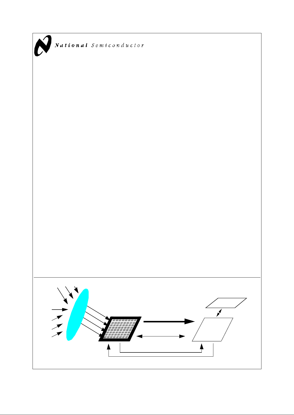
12bit digital image
lens
I2C compatible
Digital Image
Processor
Storage
snapshot
event trigger
LM9617
System Block Diagram
LM9617 Monochrome CMOS Image Sensor VGA 30 FPS
Confidential 2 www.national.com
Column CDS
APS Array
Horizontal Shif t
Register
POR
1
2 Bit A/D
AMP
Bad P ixel
Detect & Correct
Digital Video
Frame r
Black Level
Compensation
d[11:0]
pclk
hsync
vsync
Row Address
Decoder
Vertical
Horizontal
Master Timer
Timing
Timing
Row Address
Gen
Clock Gen
I2C Compatible
Register Bank
Reset
Gen
Gain
Control
Serial I/F
sda
sclk
sadr
Power
Control
pdwnsnapshot
extsync
Controller
(sequencer)
irq
mclk
Overall Chip Block Diagram
Figure 1. Chip Block Diagram
7
9
10
11
12
13
14
15
16
18
17
42
40
39
38
37
36
35
34
33
31
32
sclk
resetb
pdwn
vss_dig
vdd_dig
vsync
pclk
mclk
d1
d0
fine_i
vss_od1
vss_od3
gnd
fine_ctrl
offset
vdd_ana1
vdd_ana2
vss_ana2
sda
sadr
irq
vdd_pix
vrl
vsrvdd
extsync
vdd_od 1
6 5 4 3 2
1
48 47 46 45
NC
d4
d5
d6d8d7
d9
vdd_od2
vss_od2
19 20 21 2322 24 25 26 27 28 30
48 PIN LCC
43
d11
d10
8
snapshot
41
NC
44
vref_adc
29
d3
d2
LM9617
hsync
vss_ana1
vdd_o d3
NC
NC
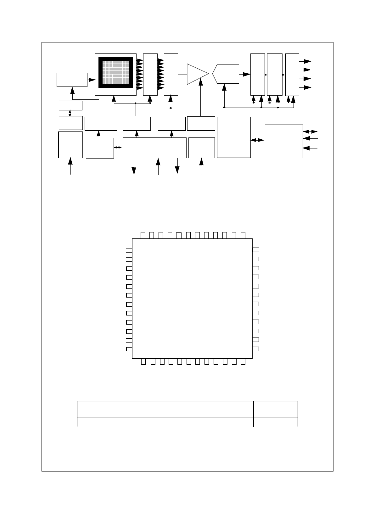
Connection Diagram
Ordering Information
Temperature
(0°C ≤ TA ≤ +50°C)
NS Package
LM9617 CCEA LCC
LM9617
Confidential 3 www.national.com
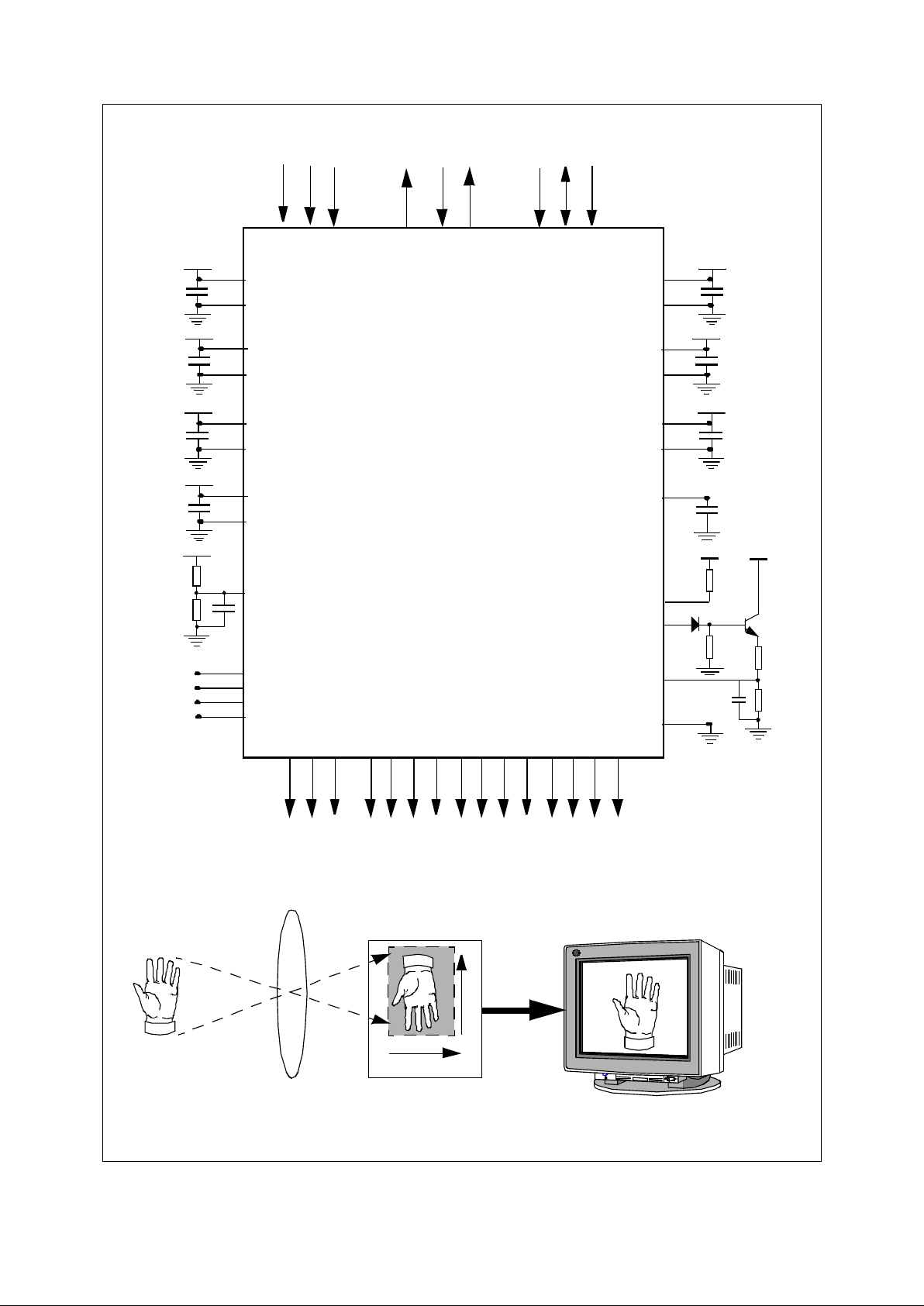
Typical Application Circuit
0.1µF
1.5k
Ω
820
Ω
3.3V analog
0.1µF
3.3V digital
12
9
37
36
35
7 6810
vss_dig
resetb
vdd_ana1
vss_ana1
vref_adc
vdd_od1
vss_od1
sadr
extsyn c
sclk
sda
d9
d8
d7d5d6
d4
d1
d0
snapshot
30 29 28 2627 25 24 23 22 21 17
d2
d3
11
vdd_dig
48 5
20
d10
d11
0.1µF
3.3V analog
31
32
vdd_od2
vss_od2
0.1µF
3.3V digital
0.1µF
3.3V digital
47
46
vdd_pix
vrl
0.1µF
3
2
1
vsrvdd
1.0µF
13 14 15
hsyn c
vsync
pclk
LM9617
pdwn
Serial Control Bus
System Control
Digital Video Bus
Camera Control
irq
4
33
34
vdd_ana2
vss_ana2
0.1µF
3.3V analog
16
mclk
vdd_od3
vss_od3
0.1µF
44
45
fine_i
41
gnd
40
3.3V analog
3.3V digital
offset
fine_ctrl
39
NC
18
NC
19
NC
42
NC
43
10kΩ
1.2kΩ
470Ω
2N3904
1N4148
4.7µF
vdd_ana
22kΩ
vdd_ana
38
1%
1%
1%
1%
Figure 2. Typical Application Diagram
Scan Read Out Direction
Figure 3. Scan directions and position of origin in imaging system
(0,0)
pin 1
CMOS Image Sensor
(0,0)
digital
out
lens
(0,0)
horizontal scan
vertical scan
LM9617

Confidential 4 www.national.com
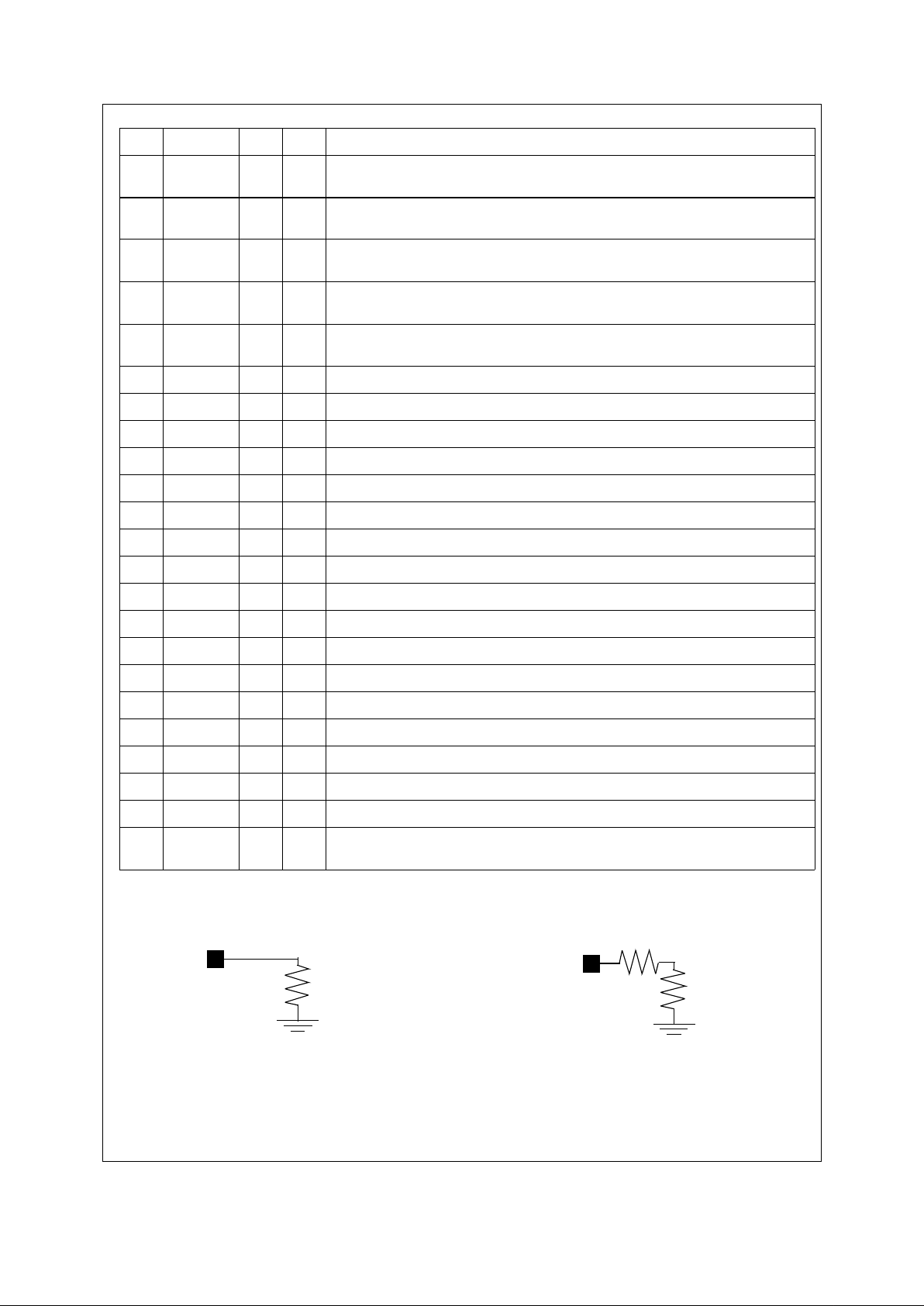
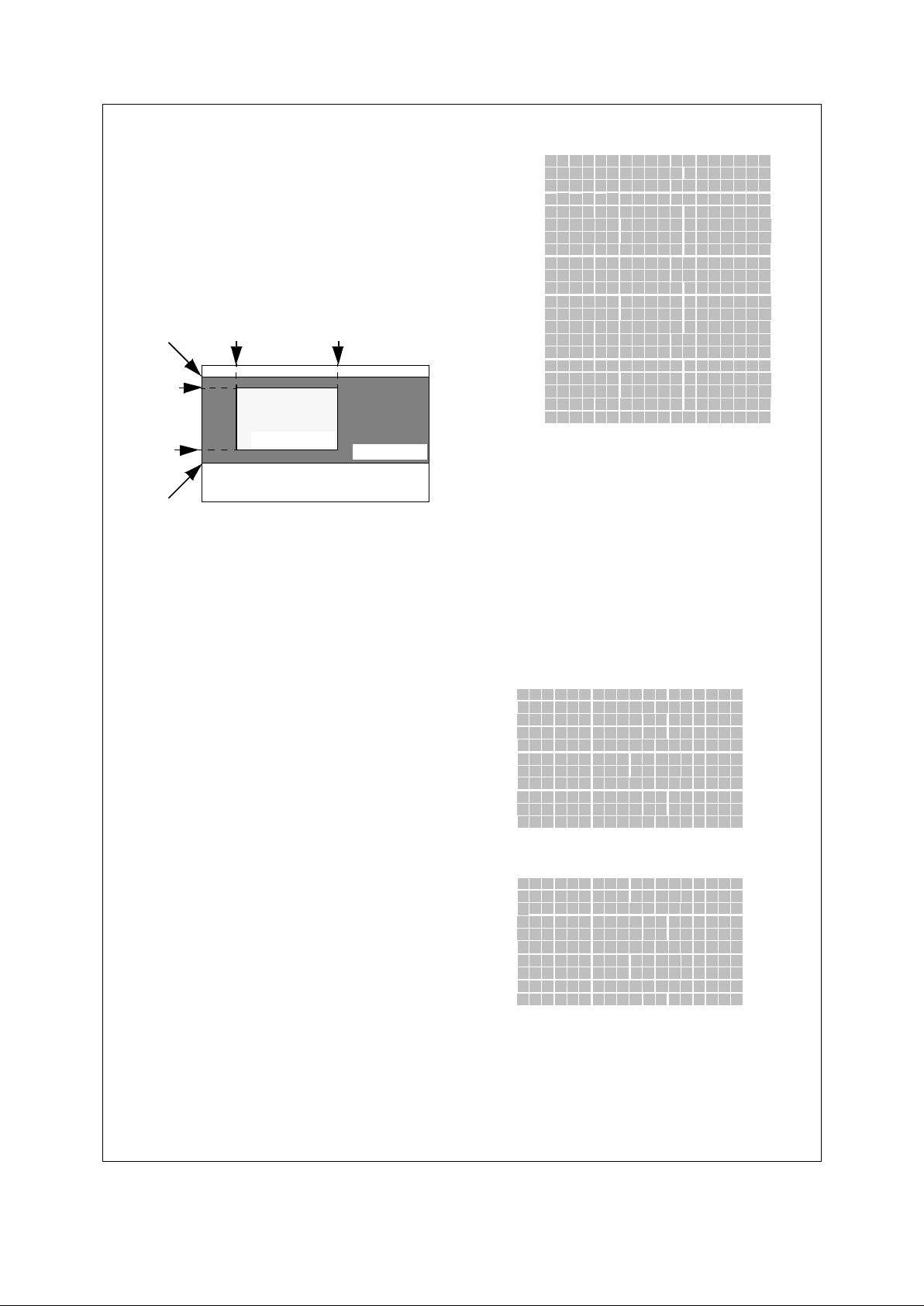
Pin Descriptions
Pin Name I/O Typ Description
1 vsrvdd I0 P
Analog bidirectional, it should be connect to ground via a 1.0µf capacitor. This pin is the
internal charge pump voltage source.
2 vrl I A Anti blooming pin. This pin is normally tied to ground.
3 vdd_pix I P 3.3 volt supply for the pixel array.
4 irq O D
Digital output, the interrupt request pin. This pin generates interrupts during snapshot
mode.
5 sadr I D
Digital input with pull down resistor. This pin is used to program different slave addresses
for the sensor in an I2C compatible system.
6 sda IO D
I2C compatible serial interface data bus. The output stage of this pin has an open drain
driver.
7 sclk I D I2C compatible serial interface clock.
8 snapshot I D Digital input with pull down resistor used to activate (trigger) a snapshot sequence.
9 resetb I D
Digital input with pull up resistor. When forced to a logic 0 the sensor is reset to its default
power up state. The resetb signal is internally synchronized to mclk which must be run-
ning for a reset to occur.
10 pdwn I D
Digital input with pull down resistor. When forced to a logic 1 the sensor is put into power
down mode.
11 vss_dig I P 0 volt power supply for the digital circuits.
12 vdd_dig I P 3.3 volt power supply for the digital circuits.
13 hsync IO D
Digital Bidirectional. This is a dual mode pin. When the sensor’s digital video port is con-
figured to be a master, (the default), this pin is an output and is the horizontal synchroni-
zation pulse. When the sensor’s digital video port is configured to be a slave, this pin is
an input and is the row trigger.
14 vsync IO D
Digital Bidirectional. This is a dual mode pin. When the sensor’s digital video port is con-
figured to be a master, (the default), this pin is an output and is the vertical synchroniza-
tion pulse. When the sensor’s digital video port is configured to be a slave, this pin is an
input and is the frame trigger.
15 pclk O D Digital output. The pixel clock.
16 mclk I D Digital input. The sensor’s master clock input.
17 d0 O D
Digital output. Bit 0 of the digital video output bus. This output can be put into tri-state
mode.
18 NC Pin not used, do not connect.
19 NC Pin not used, do not connect.
20 d1 O D
Digital output. Bit 1 of the digital video output bus. This output can be put into tri-state
mode.
21 d2 O D
Digital output. Bit 2 of the digital video output bus. This output can be put into tri-state
mode.
22 d3 O D
Digital output. Bit 3 of the digital video output bus. This output can be put into tri-state
mode.
23 d4 O D
Digital output. Bit 4 of the digital video output bus. This output can be put into tri-state
mode.
24 d5 O D
Digital output. Bit 5 of the digital video output bus. This output can be put into tri-state
mode.
25 d6 O D
Digital output. Bit 6 of the digital video output bus. This output can be put into tri-state
mode.
LM9617
Confidential 5 www.national.com
Pin Descriptions (Continued)
Legend: (I=Input), (O=Output), (IO=Bi-directional), (P=Power), (D=Digital), (A=Analog).
Figure 4. Equivalent Circuits For adc_ref and offset pins
Pin Name I/O Typ Description
26 d7 O D
Digital output. Bit 7 of the digital video output bus. This output can be put into tri-state
mode.
27 d8 O D
Digital output. Bit 8 of the digital video output bus. This output can be put into tri-state
mode.
28 d9 O D
Digital output. Bit 9 of the digital video output bus. This output can be put into tri-state
mode.
29 d10 O D
Digital output. Bit 10 of the digital video output bus. This output can be put into tri-state
mode.
30 d11 O D
Digital output. Bit 11 of the digital video output bus. This output can be put into tri-state
mode.
31 vdd_od2 I P 3.3 volt supply for the digital IO buffers.
32 vss_od2 I P 0 volt supply for the digital IO buffers
33 vdd_ana2 I P 3.3 volt supply for analog circuits.
34 vss_ana2 I P 0 volt supply for analog circuits.
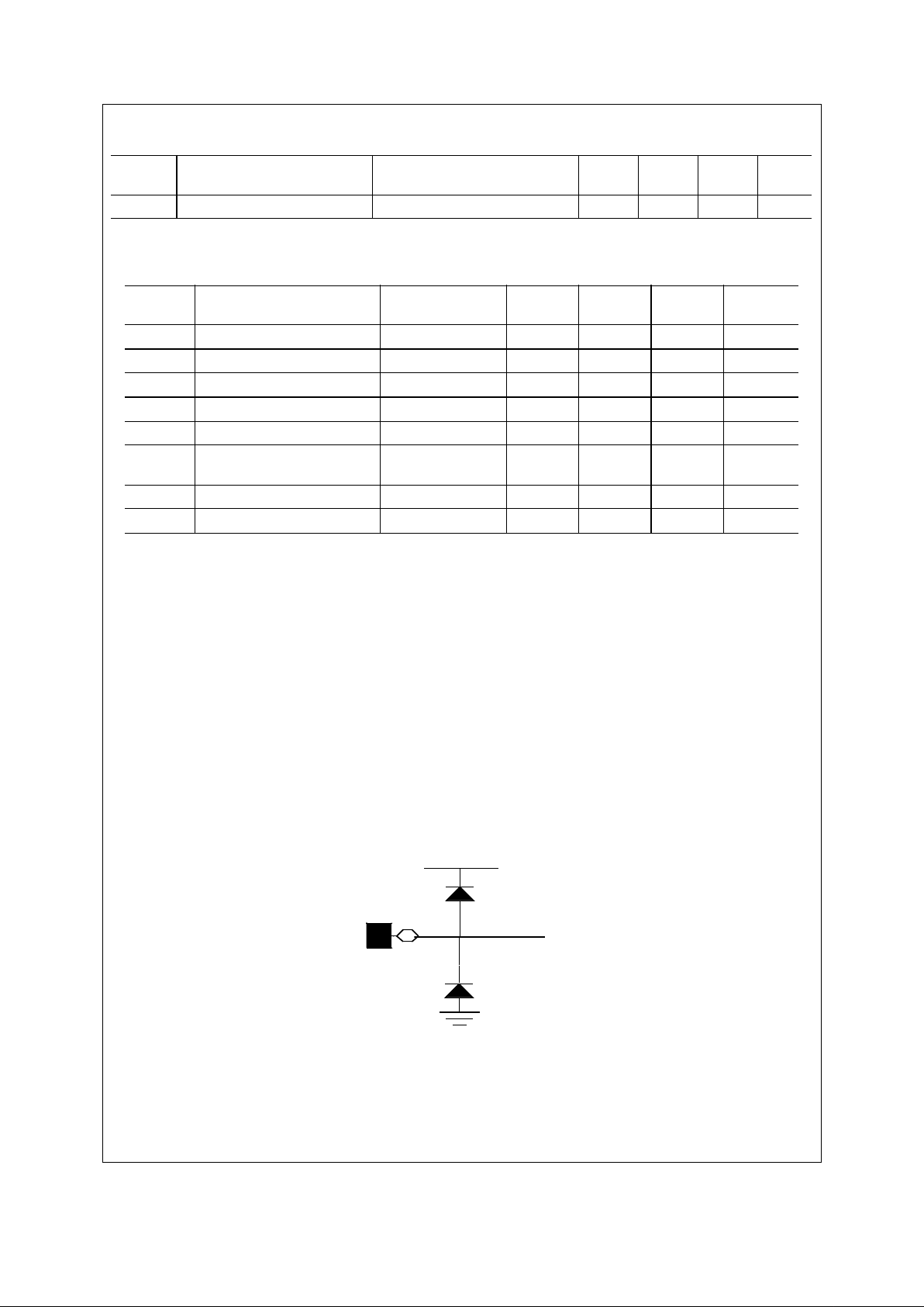
35 vref_adc I A A/D reference resistor ladder voltage. See figure 4 for equivalent circuit.
36 vss_ana1 I P 0 volt supply for analog circuits.
37 vdd_ana1 I P 3.3 volt supply for analog circuits.
38 offset I A Analog input used to adjust the offset of the sensor. See figure 4 for equivalent circuit.
39 fine_ctrl O A Analog output used to drive the offset pin.
40 gnd This pin must be tied to ground.
41 fine_i I A Bias current for the fine offset adjust.
42 NC Pin not used, do not connect.
43 NC Pin not used, do not connect.
44 vdd_od3 I P 3.3 volt supply for the sensor.
45 vss_od3 I P 0 volt supply for the sensor.
46 vss_od1 I P 0 volt supply for the digital IO buffers
47 vdd_od1 I P 3.3 volt supply for the digital IO buffers.
48 extsync O D
Digital output. The external event synchronization signal is used to synchronize external
events in snapshot mode.
800Ω
adc_vref
1KΩ
200Ω
offset
LM9617
Confidential 6 www.national.com
Absolute Maximum Ratings (Notes 1 & 2)
Any Positive Supply Voltage 6.5V
Voltage On Any Input or Output Pin -0.5V to 6.5V
Input Current at any pin (Note 3) ±25mA
ESD Susceptibility (Note 5)
Human Body Model 2000V
Machine Model 200V
Package Input Current (Note 3) ±50mA
Package Power Dissipation @ TA(Note 4) 2.5W
Soldering Temperature Infrared,
10 seconds (Note 6) 220°C
Storage Temperature -40°C to 125°C
Operating Ratings (Notes 1 & 2)
Operating Temperature Range 0°C≤T≤+50°C
All VDD Supply Voltages +3.15V to +3.6V
Voltage Range on vref_adc pin +0.6V to +1.0V
Voltage Range on offset pin +0.04V to +0.4V
DC and logic level specifications
The following specifications apply for all VDD pins= +3.3V. Boldface limits apply for TA = T
MIN
to T
MAX
: all other limits TA = 25oC
(Note 7)
Power Dissipation Specifications
The following specifications apply for All VDD pins = +3.3V. Boldface limits apply for TA = T
MIN
to T
MAX
: all other limits TA = 25oC.
Symbol Parameter Conditions
Min
note 9
Typical
note 8
Max
note 9
Units
sclk, sda, sadr, Digital Input/Output Characteristics
VIH Logical “1” Input Voltage 0.7*vdd_od vdd_od+0.5 V
VIL Logical “0” Input Voltage -0.5 0.3*vdd_od V
VOL Logical “0” Output Voltage vdd_od = +3.15V, Iout=3.0mA 0.5 V
V
hys
Hysteresis (SCLK pin only) vdd_od = +3.15V
0.05*vdd_o
d
V
I
leak
Input Leakage Current Vin=vss_od -1 mA
mclk, snapshot, pdwn, resetb, hsync, vsync Digital Input Characteristics
VIH Logical “1” Input Voltage vdd_dig = +3.6V 2.0 V
VIL Logical “0” Input Voltage vdd_dig = +3.15V 0.8 V
IIH Logical “1” Input Current VIH = vdd_dig 0.1 mA
IIL Logical “0” Input Current VIL = vss_dig -1 mA
d0 - d11, pclk, hsync, vsync, extsync, irq, Digital Output Characteristics
VOH Logical “1” Output Voltage vdd_od=3.15V, Iout=-1.6mA 2.2 V
VOL Logical “0” Output Voltage vdd_od=3.15V, Iout =-1.6mA 0.5 V
IOZ TRI-STATE Output Current
VOUT = vss_od
VOUT = vdd_od
-0.1
0.1
mA
mA
IOS Output Short Circuit Current +/-17 mA
Power Supply Characteristics
IA Analog Supply Current
Power down mode, no clock.
Operational mode in dark
700
19
mA
mA
ID Digital Supply Current
Power down mode, no clock.
Operational mode in dark
300
7
mA
mA
Symbol Parameter Conditions
Min
note 9
Typical
note 8
Max
note 9
Units
P
dwn
Power Down no clock running 5 mW
PWR Average Power Dissipation
mclk = 48Mhz & sensors default settings in dark.
90 mW
LM9617
Confidential 7 www.national.com
Video Amplifier Specifications
The following specifications apply for all VDD pins= +3.3V. Boldface limits apply for TA = T
MIN
to T
MAX
: all other limits TA = 25oC.
AC Electrical Characteristics
The following specifications apply for All VDD pins = +3.3V. Boldface limits apply for TA = T
MIN
to T
MAX
: all other limits TA = 25oC.
Note 1: Absolute Maximum Ratings indicate limits beyond which damage to the device may occur. Operating Ratings indicate con-
ditions for which the device is functional, but do not guarantee specific performance limits. For guaranteed specifications
and test conditions, see the Electrical Characteristics. The guaranteed specifications apply only for the test conditions
listed. Some performance characteristics may degrade when the device is not operated under the listed test conditions.
Note 2: All voltages are measured with respect to VSS = vss_ana = vss_od = vss_dig = 0V, unless otherwise specified.
Note 3: When the voltage at any pin exceeds the power supplies (VIN < VSS or VIN > VDD), the current at that pin should be lim-
ited to 25mA. The 50mA maximum package input current rating limits the number of pins that can safely exceed the power
supplies with an input current of 25mA.
Note 4: The absolute maximum junction temperature (TJmax) for this device is 125oC. The maximum allowable power dissipation
is dictated by TJmax, the junction-to-ambient thermal resistance (ΘJA), and the ambient temperature (TA), and can be cal-
culated using the formula PDMAX = (TJmax - TA)/ΘJA. In the 48-pin LCC, ΘJA is 38.5oC/W, so PDMAX = 2.5W at 25oC
and 1.94W at the maximum operating ambient temperature of 50oC. Note that the power dissipation of this device under
normal operation will be well under the PDMAX of the package.
Note 5: Human body model is 100pF capacitor discharged through a 1.5kΩ resistor. Machine model is 220pF discharged through
ZERO Ohms.
Note 6: See AN450, “Surface Mounting Methods and Their Effect on Product Reliability”, or the section entitled “Surface Mount”
found in any post 1986 National Semiconductor Linear Data Book, for other methods of soldering surface mount devices.
Note 7: The analog inputs are protected as shown below. Input voltage magnitude up to 500mV beyond the supply rails will not
damage this device. However, input errors will be generated If the input goes above AV+ and below AGND.
Note 8: Typical figures are at TJ = 25oC, and represent most likely parametric norms.
Note 9: Test limits are guaranteed to National's AOQL (Average Outgoing Quality Level).
Symbol Parameter Conditions
Min
note 9
Typical
note 8
Max
note 9
Units
Video Amplifier Nominal Gain 64 linear steps 0-15 dB
Symbol Parameter Conditions
Min
note 9
Typical
note 8
Max
note 9
Units
F
mclk
Input Clock Frequency 12 48 MHz
T
ch
Clock High Time @ CLK
max
10 45 ns
T
cl
Clock Low Time @ CLK
max
10 45 ns
Clock Duty Cycle @ CLK
max
45/55 55/45 min/max
Trc, TfcClock Input Rise and Fall Time 3 ns
F
hclk
Internal System Clock Frequency
1.0 14.0 MHz
T
reset
Reset pulse width 1.0 µs
FRM
rate
Frame Rate 1 30 fps
IOP
Pad
VDD
VSS
Internal Circuits
LM9617
Confidential 8 www.national.com
CMOS Active Pixel Array Specifications
Image Sensor Specifications
The following specifications apply for All VDD pins = +3.3V, TA = 25oC, Illumination Color Temperature = 2850oK, IR cutoff filter at
700nm, mclk = 48MHz, frame rate = 30Hz, vref_adc = 0.6 volt, video gain 0dB.
Note 1: Typical figures are at TJ = 25oC, and represent most likely parametric norms.
Parameter Value Units
Number of pixels (column, row)
Total
Active
664 x 504
648 x 488
pixels
pixels
Array size (x,y Dimensions)
Total
Active
4.98 x 3.78
4.86 x 3.66
mm
mm
Pixel Pitch 7.5 µ
Fill Factor (without micro-lens) 47 %
Parameter Conditions
Min Typical
note 1
Max Units
Optical Sensitivity @ A/D output 28.7 kLSBs/(lux.s)
Optical Sensitivity @ A/D input
4.13
volt/(lux.s)
Dynamic Range 57 dB
Read Noise 5.3 LSBs
Offset Fixed Pattern Noise
RMS value of pixel FPN in dark
as a percentage of full scale.
0.35 %
Sensitivity Fixed Pattern Noise
RMS variation of pixel sensitivities as a percentage of the average sensitivity.
1 %
LM9617
Confidential 9 www.national.com
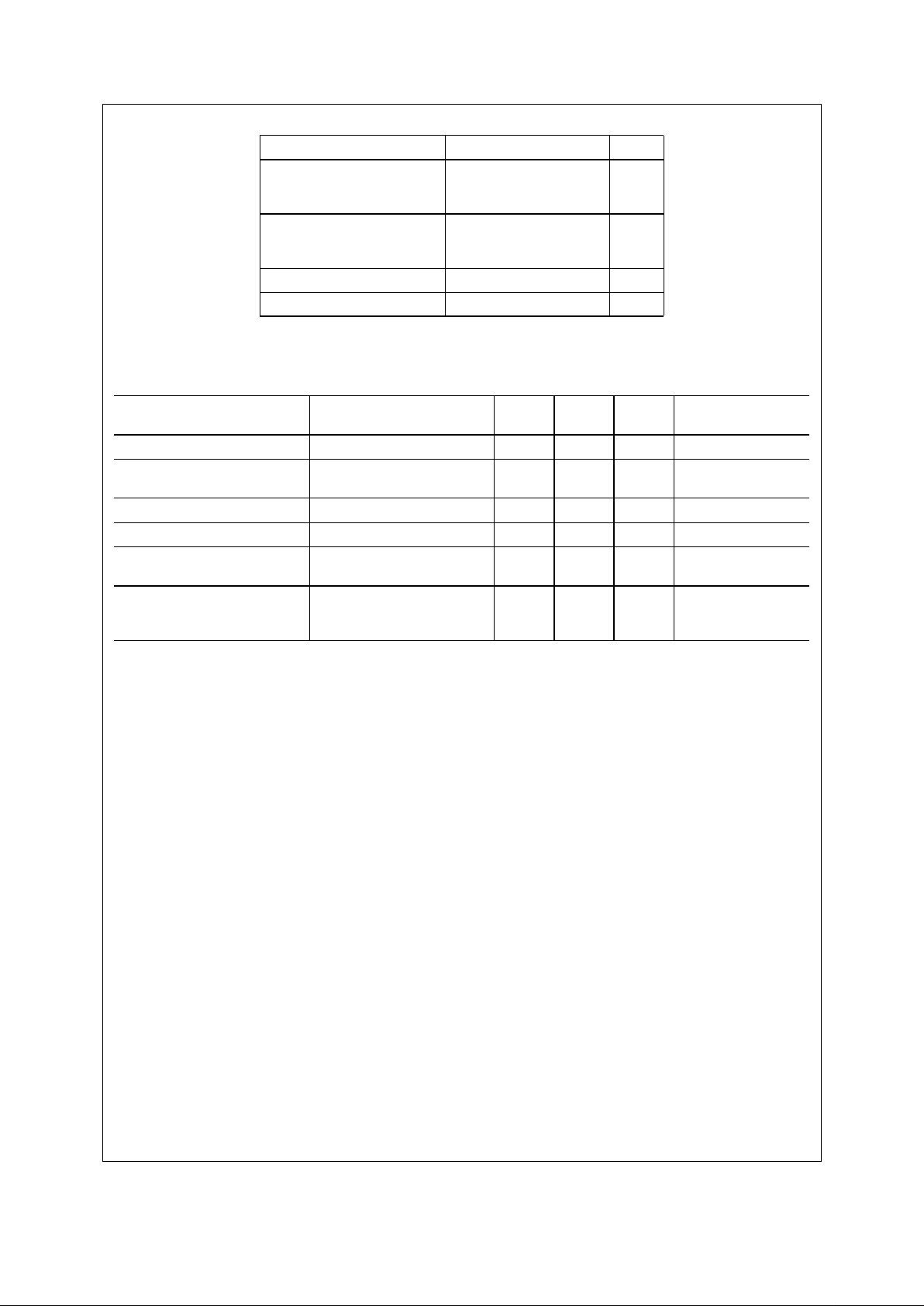
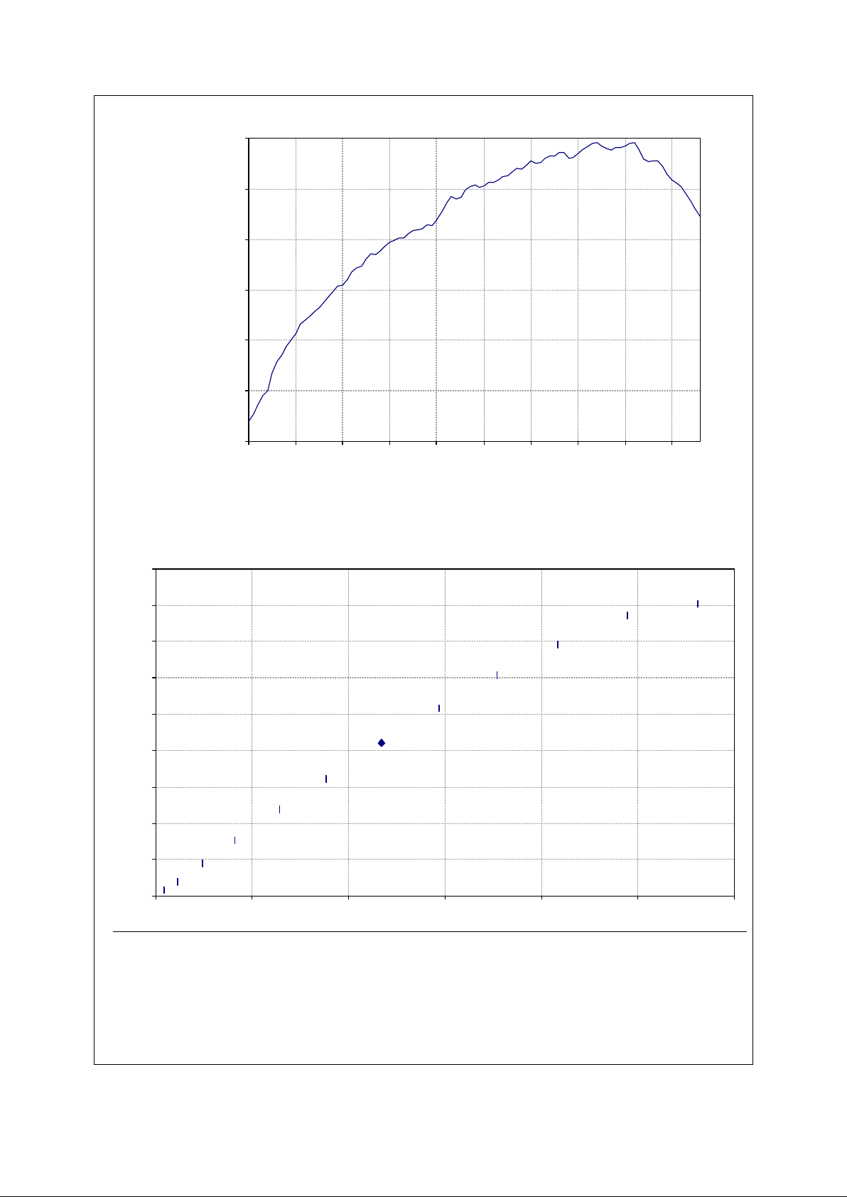
Sensor Response Curves
0.00E+00
2.00E+02
4.00E+02
6.00E+02
8.00E+02
1.00E+03
1.20E+03
370 420 470 520 570 620 670 720 770 820
wavelength [nm]
Spectral sensitivity [V/((W/m^2)*s)]
Figure 5. Spectral Response Curve
0
500
1000
1500
2000
2500
3000
3500
4000
4500
0 0.05 0.1 0.15 0.2 0.25 0.3
Exposure (lux.sec)
A/D output code
Figure 6. Linearity Response Curve
LM9617
Confidential 10 www.national.com
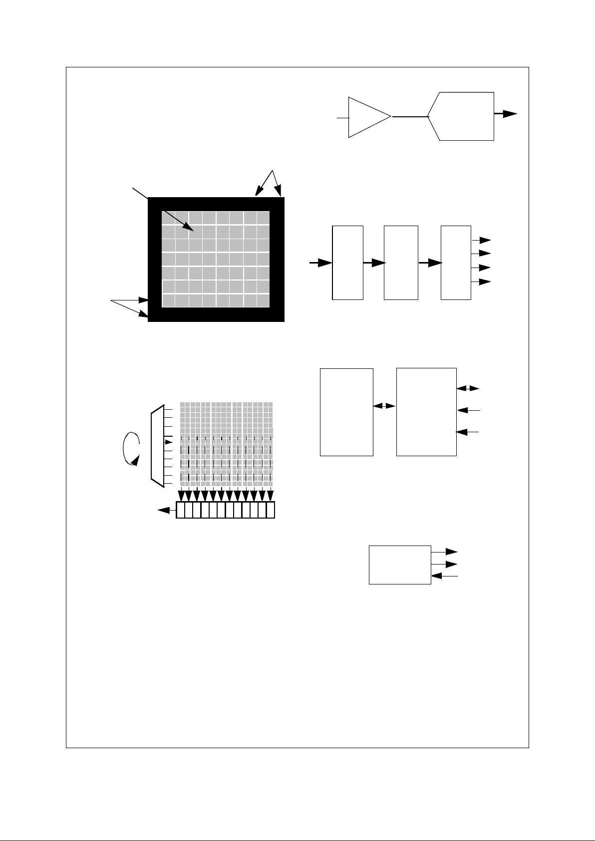
Functional Description
1.0 OVERVIEW
1.1 Light Capture and Conversion
The LM9617 contains a CMOS active pixel array consisting of
648 rows by 488 columns. This active region is surrounded by 8
columns and 8 rows of optically shielded (black) pixels as shown
in Figure.
8 columns, 8 rows
black pixels
8 columns, 8 rows
black pixels
648 columns, 488 rows
mono-chrome active pixels
Figure 7: CMOS APS region of the LM9617
At the beginning of a given integration time the on-board timing
and control circuit will reset every pixel in the array one row at a
time as shown in Figure 8. Note that all pixels in the same row
are simultaneously reset, but not all pixels in the array.
a b c d e f g h i j k l m n o p q r
0
1
2
3
4
5
6
7
8
9
10
11
12
14
13
15
CDS/Shift Register
Line Address
Analog Data Out
Figure 8: CMOS APS Row and Column addressing scheme
At the end of the integration time, the timing and control circuit
will address each row and simultaneously transfer the integrated
value of the pixel to a correlated double sampling circuit and
then to a shift register as shown in Figure 8.
Once the correlated double sampled data has been loaded into
the shift register, the timing and control circuit will shift them out
one pixel at a time starting with column “a”.
The pixel data is then fed into an analog video amplifier, where a
user programmed gain is applied .
After gain adjustment the analog value of each pixel is converted to a 12 bit digital data as shown in Figure 9.
12 Bit A/D
Video
AMP
Analog pixel values Digital pixel data
0-15dB
Figure 9: Analog Signals In, Digital Data Out.
The digital pixel data is further processed to:
• remove defects due to bad pixels,
• compensate black level, before being framed and presented
on the digital output port. (see Figure 10).
Figure 10. Digital Pixel Processing.
1.2 Program and Control Interfaces
The programming, control and status monitoring of the LM9617
is achieved through a two wire I2C compatible serial bus. In
addition, a slave address pin is provided (see Figure 11).
Figure 11. Control Interface to the LM9617.
Additional control and status pins: snapshot and external event
synchronization are provided allowing the latency of the serial
control port to be bypassed during single frame capture. An
interrupt request pin is also available allowing complex snapshot
operations to be controlled via an external micro-processor (see
Figure 12).
Figure 12. Snapshot & External Event Trigger Signals
Bad Pixel
Correction
Digital Video
Framer
Black Level
Compensation
do[11:0]
pclk
hsync
vsync
I2C Compatible
Register Bank
Serial I/F
sda
sclk
sadr
Timing
Generator
irq
snapshot
extsyn
LM9617
Confidential 11 www.national.com
Functional Description (continued)
2.0 WINDOWING
The integrated timing and control circuit allows any size window
in any position within the active region of the array to be read out
with a 1x1 pixel resolution. The window read out is called the
“Display Window”.
A “Scan Window” must be defined first, by programing the start
and end row addresses as shown in Figure 13. Four coordinates
(start row address, start column address, end row address &
end column address) are programmed to define the size and
location of the “Display Window” to be read out (see Figure 13).
Figure 13. Windowing
Notes:
• The “Display Window” must always be defined within the
“Scan Window”.
• A “Display Window” can only be read out in the progressive
scan mode.
• By default the “Display Window” is the complete array.
2.1 Programming the scan window
Two registers (SROWS & SROWE) are provided to program the
size of the scan window. The start and end row address of the
scan window is given by:
Where:
SwStartRow
is the contents of the Scan Window start row
register (SROWS)
SwEndROW
is the contents of the Scan Window end row register (SROWE)
SwLsb
is bit 6 of the Display Window LSB register
(DWLSB)
2.2 Programming the display window
Five register (DROWS, DROWE, DCOLS, DCOLE and DWLSB)
are provided to program the display window as described in the
register section of this datasheet.
3.0 READ OUT MODES
3.1 Progressive Scan Readout Mode
In progressive scan readout mode, every pixel in every row in
the display window is consecutively read out, one pixel at a time,
starting with the left most pixel in the top most row. Hence, for
the example shown in Figure 13, the read out order will be
a0,b0,...,r0 then a1,b1,...,r1 and so on until pixel r20 is read out.
a b c d e f g h i j k l mn o p q r
1
2
3
4
5
6
7
8
9
10
11
12
13
15
14
16
17
18
19
20
Row/Vertical
0
Column/Horizontal
Figure 14: Progressive Scan Read Out Mode
3.2 Interlaced Readout Mode
In interlaced readout mode, pixels are read out in two fields, an
Odd Field followed by an Even Field.
The Odd Field, consisting of all even rows contained within the
display window, is read out first. Each pixel in the “Odd Field” is
consecutively read out, one pixel at a time, starting with the left
most pixel in the top most even row.
The Even Field, consisting of all odd rows contained within the
display window, is then read out. Each pixel in the “Even Field”
is consecutively read out, one pixel at a time, starting with the
left most pixel in the top most odd row.
a b c d e f g h i j k l mn o p q r
2
4
6
8
10
12
14
16
18
20
0
Row/Vertical
Column/Horizontal
Odd Field
1
3
5
9
7
11
13
15
17
19
Row/Vertical
Column/Horizontal
Even Field
a b c d e f g h i j k l mn o p q r
Figure 15: Interlace Read Out Mode
Hence, for the example shown in Figure , the display window is
broken up into two fields, as shown in Figure . Pixels a0,b0,...,r0
followed by a2,b2,...,r2 and so on until pixels a20,b20,...r20 in
the even field are read out first. The even field read out is followed by pixels in the odd field, a1,b1,...,r1 then a3,b3,...,r3 until
pixels a19,b19,...,r19.
display row
Active Pixel Array
Display Window
Scan Window
display row
display col
display col
start address
end address
start address
end address
scan row
start address
scan row
end address
scan row start address = (2* SwStartRow) + SwLsb
scan row end address = (2* SwEndRow) + 1 + SwLsb
LM9617
Confidential 12 www.national.com
Functional Description (continued)
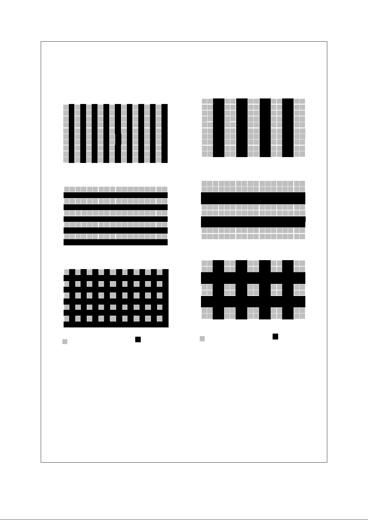
4.0 SUBSAMPLING MODES
4.1 2:1 Sub-Sampling
The timing and control circuit can be programmed to sub-sample pixels in the display window vertically, horizontally or both,
with an aspect ratio of 2:1 as illustrated in Figure16
0
1
2
3
4
5
6
7
8
9
Column/Horizontal
a b c d e f g h i j k l l n o p q r
a b c d e f g h i j k l m n o p
0
1
2
3
4
5
6
7
8
9
b) Vertical Sub-Sampling
Row/Vertical
Column/Horizontal
q
r
a b c d e f g h i j k l m n o p q r
0
1
2
3
4
5
6
7
8
Column/Horizontal
Row/Vertical
9
a) Horizontal Sub-Sampling
c) Horizontal & Vertical Sub-Sampling
Read Out
Not Read Out
Row/Vertical
Figure 16: 2:1 Horizontal and Vertical Sub-Sampling
4.2 4:2 Sub-Sampling
The timing and control circuit can be programmed to sub-sample pixels in the display window vertically, horizontally or both,
with an aspect ratio of 4:2 as illustrated in Figure17.
Column/Horizontal
a) Horizontal Sub-sampling
Read Out
Not Read Out
a b c d e f g h i j k l m n o p q r
0
1
2
3
4
5
6
7
8
9
Row/Vertical
a b c d e f g h i j k l m n o p q r
0
1
2
3
4
5
6
7
8
9
Column/Horizontal
Row/Vertical
a b c d e f g h i j k l m n o p q r
0
1
2
3
4
5
6
7
8
9
Column/Horizontal
Row/ Vertica l
c) Horizontal & Vertical Sub-sampling
b) Vertical Sub-sampling
Figure 17: 4:2 Horizontal and Vertical Sub-Sampling
LM9617
 Loading...