

NSC LM9140BYZ-5.0, LM9140BYZ-4.1, LM9140BYZ-2.5, LM9140BYZ-10.0 Datasheet
LM9140
Precision Micropower Shunt Voltage Reference
General Description
The LM9140’s reverse breakdown voltage temperature coefficients of
±
25 ppm/˚C are ideal for precision applications.
The LM9140’s advanced design eliminates the need for an
external stabilizing capacitor while ensuring stability with any
capacitive load, thus making the LM9140 easy to use. Further reducing design effort is the availability of several fixed
reverse breakdown voltages: 2.500V, 4.096V, 5.000V, and
10.000V. The minimum operating current increases from
60 µA for the LM9140-2.5 to 100µAforthe LM9140-10.0.All
versions have a maximum operating current of 15 mA.
The LM9140 utilizes fuse and zener-zap reverse breakdown
voltage trim during wafer sort to ensure that the prime parts
have an accuracy of better than
±
0.5%(B grade) at 25˚C.
Bandgap reference temperature drift curvature correction
and low dynamic impedance ensure stable reverse breakdown voltage accuracy over a wide range of operating temperatures and currents.
Features
n Guaranteed temperature coefficient of±25 ppm/˚C
n Reverse breakdown voltage tolerance of
±
0.5
%
n Small package: TO-92
n No output capacitor required
n Tolerates capacitive loads
n Fixed reverse breakdown voltages of 2.500V, 4.096V,
5.000V, and 10.000V
Key Specifications
(LM9140-2.5)
n Temperature coefficient:
±
25 ppm/˚C (max)
n Output voltage tolerance:
±
0.5%(max)
n Low output noise (10 Hz to 10 kHz): 35 µV
rms
(typ)
n Wide operating current range: 60 µA to 15 mA
n Industrial temperature range: −40˚C to +85˚C
Applications
n Portable, Battery-Powered Equipment
n Data Acquisition Systems
n Instrumentation
n Process Control
n Energy Management
n Product Testing
n Automotive
n Precision Audio Components
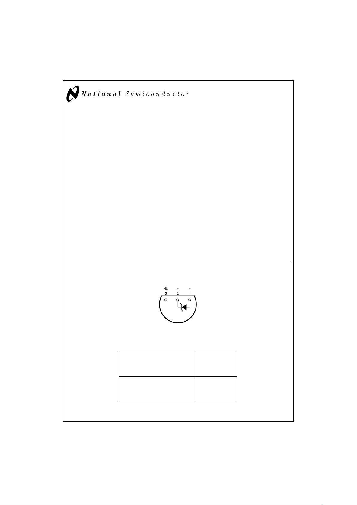
Connection Diagram
Ordering Information
Reverse Breakdown
Voltage Tolerance at 25˚C Z (TO-92)
and Average Reverse Breakdown
Voltage Temperature Coefficient
0.5%, 25 ppm/˚C max LM9140BYZ-2.5,
LM9140BYZ-4.1,
LM9140BYZ-5.0,
LM9140BYZ-10.0
TO-92
DS011393-2
Bottom View
See NS Package Number Z03A
April 1998
LM9140 Precision Micropower Shunt Voltage Reference
© 1998 National Semiconductor Corporation DS011393 www.national.com
Absolute Maximum Ratings (Note 1)
If Military/Aerospace specified devices are required,
please contact the National Semiconductor Sales Office/
Distributors for availability and specifications.
Reverse Current 20 mA
Forward Current 10 mA
Power Dissipation (T
A
=
25˚C) (Note 2)
Z Package 550 mW
Storage Temperature −65˚C to +150˚C
Lead Temperature
Z Package
Soldering (10 seconds) +260˚C
ESD Susceptibility
Human Boddy Mode (Note 3) 2 kV
Machine Model (Note 3) 200V
Operating Ratings (Notes 1, 2)
Temperature Range
(T
min
≤ TA≤ T
max
) −40˚C ≤ TA≤ +85˚C
Reverse Current
LM9140-2.5 60 µA to 15 mA
LM9140-4.1 68 µA to 15 mA
LM9140-5.0 74 µA to 15 mA
LM9140-10.0 100 µA to 15 mA
LM9140BYZ-2.5
Electrical Characteristics
Boldface limits apply for T
A
=
T
J
=
T
MIN
to T
MAX
; all other limits T
A
=
T
J
=
25˚C
Symbol Parameter Conditions Typical Limits Units
(Note 4) (Note 5) (Limit)
V
R
Reverse Breakdown Voltage I
R
=
100 µA 2.500 V
Reverse Breakdown Voltage I
R
=
100 µA
±
12.5 mV (max)
Tolerance (Note 6)
±
16.6 mV (max)
I
RMIN
Minimum Operating Current 45 µA
60 µA (max)
65 µA (max)
∆V
R
/∆T Average Reverse Breakdown I
R
=
10 mA
±
10 ppm/˚C
Voltage Temperature I
R
=
1mA
±
10
±
25 ppm/˚C (max)
Coefficient (Note 7) I
R
=
100 µA
±
10 ppm/˚C
∆V
R
/∆I
R
Reverse Breakdown Voltage I
RMIN
≤ IR≤ 1 mA 0.3 mV
Change with Operating 0.8 mV (max)
Current Change 1.0 mV (max)
1mA≤I
R
≤15 mA 2.5 mV
6.0 mV (max)
8.0 mV (max)
Z
R
Reverse Dynamic Impedance I
R
=
1 mA, f=120 Hz, 0.3 Ω
I
AC
=
0.1 I
R
0.8 Ω (max)
e
N
Wideband Noise I
R
=
100 µA 35 µV
rms
10 Hz ≤ f ≤ 10 kHz
∆V
R
Reverse Breakdown Voltage t=1000 hrs
Long Term Stability T=25˚C
±
0.1˚C 120 ppm
I
R
=
100 µA
LM9140BYZ-4.1
Electrical Characteristics
Boldface limits apply for T
A
=
T
J
=
T
MIN
to T
MAX
; all other limits T
A
=
T
J
=
25˚C
Symbol Parameter Conditions Typical Limits Units
(Note 4) (Note 5) (Limit)
V
R
Reverse Breakdown Voltage I
R
=
100 µA 4.096 V
Reverse Breakdown Voltage I
R
=
100 µA
±
20.5 mV (max)
Tolerance (Note 6)
±
27.1 mV (max)
www.national.com 2
Electrical Characteristics (Continued)
Boldface limits apply for T
A
=
T
J
=
T
MIN
to T
MAX
; all other limits T
A
=
T
J
=
25˚C
Symbol Parameter Conditions Typical Limits Units
(Note 4) (Note 5) (Limit)
I
RMIN
Minimum Operating Current 50 µA
68 µA (max)
73 µA (max)
∆V
R
/∆T Average Reverse Breakdown I
R
=
10 mA
±
10 ppm/˚C
Voltage Temperature I
R
=
1mA
±
10
±
25 ppm/˚C (max)
Coefficient (Note 7) I
R
=
100 µA
±
10 ppm/˚C
∆V
R
/∆I
R
Reverse Breakdown Voltage I
RMIN
≤ IR≤ 1 mA 0.5 mV
Change with Operating 0.9 mV (max)
Current Change 1.2 mV (max)
1mA≤I
R
≤15 mA 3.0 mV
7.0 mV (max)
10.0 mV (max)
Z
R
Reverse Dynamic Impedance I
R
=
1 mA, f=120 Hz, 0.5 Ω
I
AC
=
0.1 I
R
1.0 Ω(max)
e
N
Wideband Noise I
R
=
100 µA 80 µV
rms
10 Hz ≤ f ≤ 10 kHz
∆V
R
Reverse Breakdown Voltage t=1000 hrs
Long Term Stability T=25˚C
±
0.1˚C 120 ppm
I
R
=
100 µA
LM9140BYZ-5.0
Electrical Characteristics
Boldface limits apply for T
A
=
T
J
=
T
MIN
to T
MAX
; all other limits T
A
=
T
J
=
25˚C
Symbol Parameter Conditions Typical Limits Units
(Note 4) (Note 5) (Limit)
V
R
Reverse Breakdown Voltage I
R
=
100 µA 5.000 V
Reverse Breakdown Voltage I
R
=
100 µA
±
25.0 mV (max)
Tolerance (Note 6)
±
33.1 mV (max)
I
RMIN
Minimum Operating Current 55 µA
74 µA (max)
80 µA (max)
∆V
R
/∆T Average Reverse Breakdown I
R
=
10 mA
±
10 ppm/˚C
Voltage Temperature I
R
=
1mA
±
10
±
25 ppm/˚C (max)
Coefficient (Note 7) I
R
=
100 µA
±
10 ppm/˚C
∆V
R
/∆I
R
Reverse Breakdown Voltage I
RMIN
≤ IR≤ 1 mA 0.5 mV
Change with Operating 1.0 mV (max)
Current Change 1.4 mV (max)
1mA≤I
R
≤15 mA 3.5 mV
8.0 mV (max)
12.0 mV (max)
Z
R
Reverse Dynamic Impedance I
R
=
1 mA, f=120 Hz, 0.5 Ω
I
AC
=
0.1 I
R
1.1 Ω(max)
e
N
Wideband Noise I
R
=
100 µA 80 µV
rms
10 Hz ≤ f ≤ 10 kHz
3 www.national.com
Electrical Characteristics (Continued)
Boldface limits apply for T
A
=
T
J
=
T
MIN
to T
MAX
; all other limits T
A
=
T
J
=
25˚C
Symbol Parameter Conditions Typical Limits Units
(Note 4) (Note 5) (Limit)
∆V
R
Reverse Breakdown Voltage t=1000 hrs
Long Term Stability T=25˚C
±
0.1˚C 120 ppm
I
R
=
100 µA
LM9140BYZ-10.0
Electrical Characteristics
Boldface limits apply for T
A
=
T
J
=
T
MIN
to T
MAX
; all other limits T
A
=
T
J
=
25˚C
Symbol Parameter Conditions Typical Limits Units
(Note 4) (Note 5) (Limit)
V
R
Reverse Breakdown Voltage I
R
=
150 µA 10.00 V
Reverse Breakdown Voltage I
R
=
100 µA
±
50.0 mV (max)
Tolerance (Note 6)
±
66.3 mV (max)
I
RMIN
Minimum Operating Current 75 µA
100 µA (max)
103 µA (max)
∆V
R
/∆T Average Reverse Breakdown I
R
=
10 mA
±
10 ppm/˚C
Voltage Temperature I
R
=
1mA
±
10
±
25 ppm/˚C (max)
Coefficient (Note 7) I
R
=
150 µA
±
10 ppm/˚C
∆V
R
/∆I
R
Reverse Breakdown Voltage I
RMIN
≤ IR≤ 1 mA 0.8 mV
Change with Operating 1.6 mV (max)
Current Change 3.5 mV (max)
1mA≤I
R
≤15 mA 8.0 mV
12.0 mV (max)
23.0 mV (max)
Z
R
Reverse Dynamic Impedance I
R
=
1 mA, f=120 Hz, 0.7 Ω
I
AC
=
0.1 I
R
1.7 Ω(max)
e
N
Wideband Noise I
R
=
150 µA 180 µV
rms
10 Hz ≤ f ≤ 10 kHz
∆V
R
Reverse Breakdown Voltage t=1000 hrs
Long Term Stability T=25˚C
±
0.1˚C 120 ppm
I
R
=
150 µA
Note 1: Absolute MaximumRatings indicate limits beyond which damage to the device may occur. Operating Ratings indicate conditions for which the device is functional, but do not guarantee specific performance limits. For guaranteed specifications and test conditions, see the Electrical Characteristics. The guaranteed specifications apply only for the test conditions, see the Electrical Characteristics. The guaranteed specifications apply only for the test conditions listed. Some performance characteristics may degrade when the device is not operated under the listed test conditions.
Note 2: The maximum power dissipation must be derated at elevated temperatures and is dictated by T
Jmax
(maximum junction temperature), θJA(junction to am-
bient thermal resistance), and T
A
(ambient temperature). The maximum allowable power dissipation at any temperature is PD
MAX
=
(T
Jmax−TA
)/θJAor the number
given in the Absolute Maximum Ratings, whichever is lower. For the LM9140, T
Jmax
=
125˚C, and the typcial thermal resistance (θ
JA
), when board mounted, is
170˚C/W with 0.125" lead length for the TO-92 package.
Note 3: The human body model is a 100 pF capacitor discharged through a 1.5 kΩ resistor into each pin. The machine mode is a 200 pF capacitor discharged di-
rectly into each pin.
Note 4: Typicals are at T
J
=
25˚C and represent most likely parametric norm.
Note 5: Limits are 100%production tested at 25˚C. Limits over temperature are guaranteed through correlation using Statistical Quality Control (SQC) methods. The
limits are used to calculate National’s AOQL.
Note 6: The boldface (over-temperature) limit for Reverse Breakdown Voltage Tolerance is defined as a room termperature Reverse Breakdown Voltage Tolerance
±
[∆VR/∆T) (65˚C) (VR)]. ∆VR/∆T is the VRtemperature coefficent, 65˚C is the temperature range from −40˚C to the reference point of 25˚C, and VRis the reverse
breakdown voltage. The total over-temperature tolerence for the different grades is shown below:
B-grade:
±
0.66
%
=
±
0.5
%
±
25 ppm/˚C x 65˚C
Therefore, as an example, the B-grade LM9140-2.5 has an over-temperature Reverse Breakdown Voltage tolerance of
±
2.5V x 0.66
%
=
±
16.6 mV.
Note 7: The average temperature coefficient is defined as the maximum deviation of reference voltage at all measured temperatures between the operating T
MAX
and T
MIN
, divided by T
MAX−TMIN
. The measured temperatures are −55˚C, −40˚C, 0˚C, 25˚C, 70˚C, 85˚C and 125˚C.
www.national.com 4
 Loading...