

NSC LM9070T, LM9070SX, LM9070S Datasheet
LM9070
Low-Dropout System Voltage Regulator with Keep-Alive
ON/OFF Control
General Description
The LM9070 is a 5V,3%accurate, 250 mA low-dropout voltage regulator. The regulator features an active low delayed
reset output flag which can be used to reset a microprocessor system on turn-ON and in the event that the regulator
output falls out of regulation for any reason. An external capacitor programs a delay time interval before the reset output can return high.
Designed for automotive application the LM9070 contains a
variety of protection features such as reverse battery,
over-voltage shutdown, thermal shutdown, input transient
protection and a wide operating temperature range.
A unique two-inputlogiccontrolschemeisusedtoenableor
disable the regulator output. An ON/OFF input can be provided by an ignition switch derived signal while a second,
Keep-Alive input, is generated by a system controller. This
allows for a system to remain ON after ignition has been
switched OFF. The system controller can then execute a
power-down routine and after which command the regulator
OFF to a low quiescent current state (60 µA max).
Design techniques have been employed to allow the regulator toremainoperational and not generate false reset signals
when subjected to high levels of RF energy (300V/m from
2 MHz to 400 MHz).
Features
n Automotive application reliability
n 3%output voltage tolerance
n Insensitive to radiated RFI
n Dropout voltage less than 800 mV with 250 mA output
current
n Externally programmed reset delay interval
n Keep-alive feature with 2 logic control inputs
n 60V Load dump transient protection
n Thermal shutdown
n Short circuit protection and disable safety features
n Reverse battery protection
n Low OFF quiescent current, 50 µA maximum
n Wide operating temperature range −40˚C to +125˚C
n TO-263 and 20-pin power surface mount packages
n Lead form compatible with TLE4267 TO-220 regulator
(package TA07D)
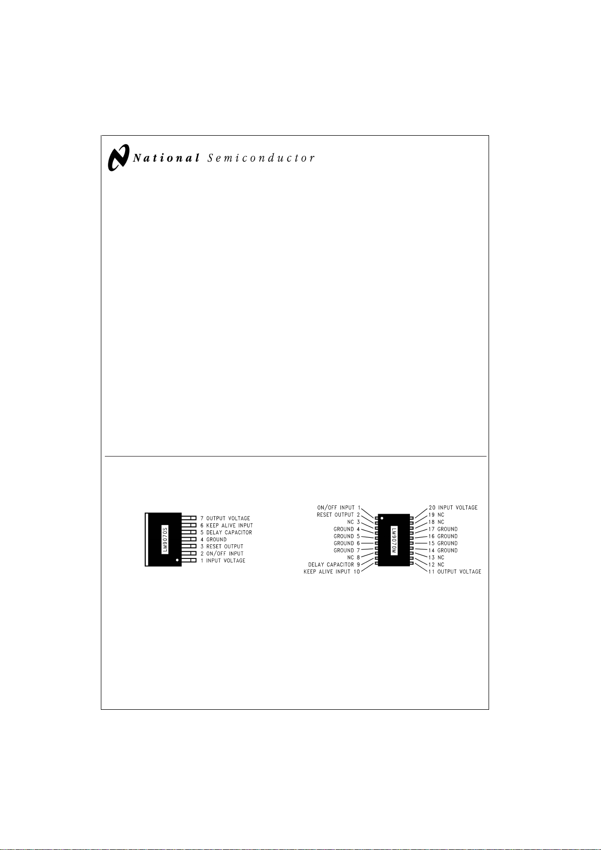
Connection Diagrams and Ordering Information (Top View)
7-Lead TO-263
Surface Mount Package
DS012831-1
Backside metal is internally connected to ground.
Order Number LM9070S
See NS Package Number TS7B
20-Pin SO Package
DS012831-2
Order Number LM9070M
See NS Package Number M20B
December 1999
LM9070 Low-Dropout System Voltage Regulator with Keep-Alive ON/OFF Control
© 1999 National Semiconductor Corporation DS012831 www.national.com
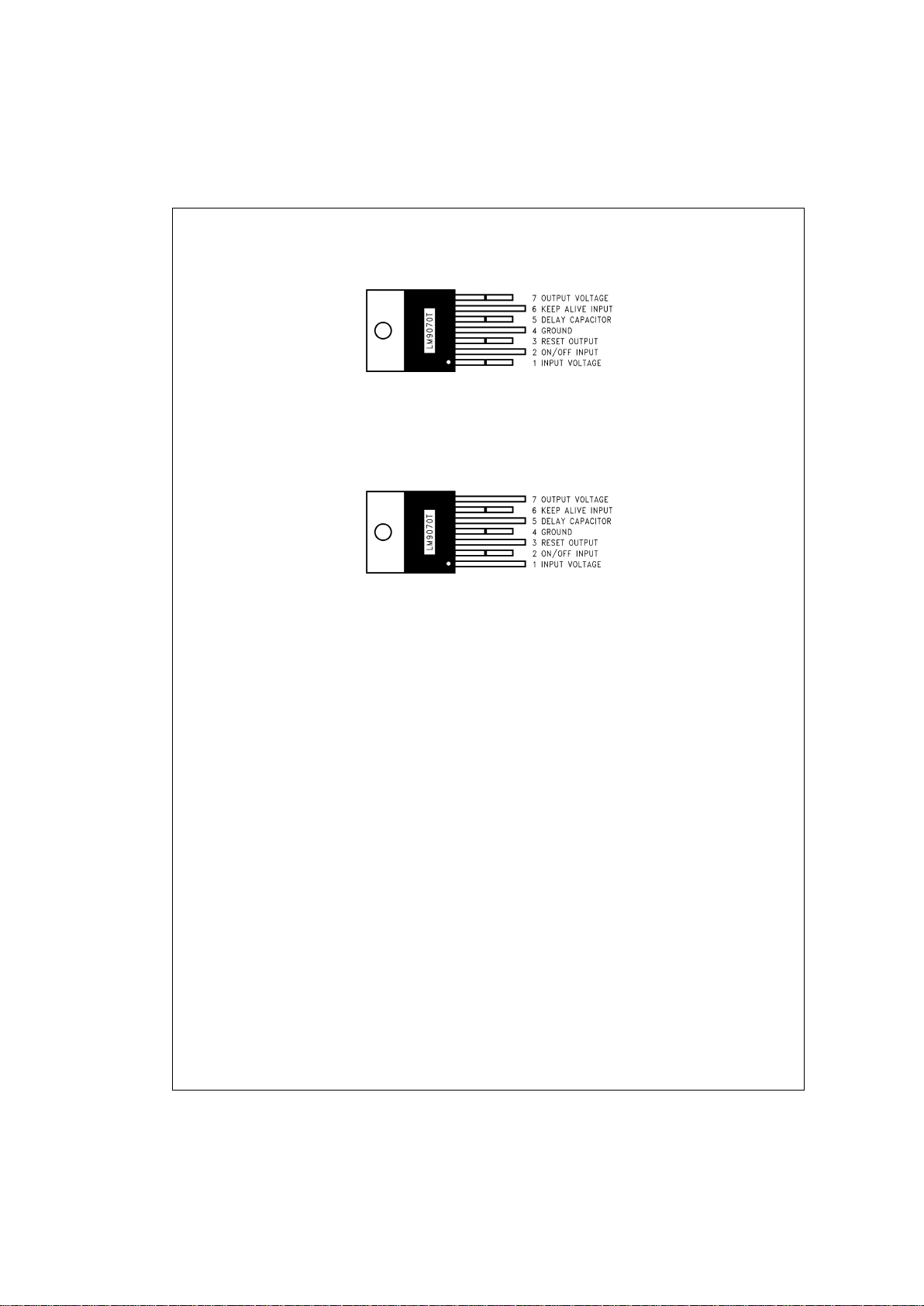
Connection Diagrams and Ordering Information (Top View) (Continued)
7-Lead TO-220 Package
(Odd numbered pins bent forward away from package body)
DS012831-3
Tab is internally connected to ground.
Order Number LM9070T
See NS Package Number TA07B
7-Lead TO-220 Package
(Even numbered pins bent forward
away from package body)
DS012831-4
Tab is internally connected to ground.
Order Number LM9070T/Flow LB09
See NS Package Number TA07D
LM9070
www.national.com 2
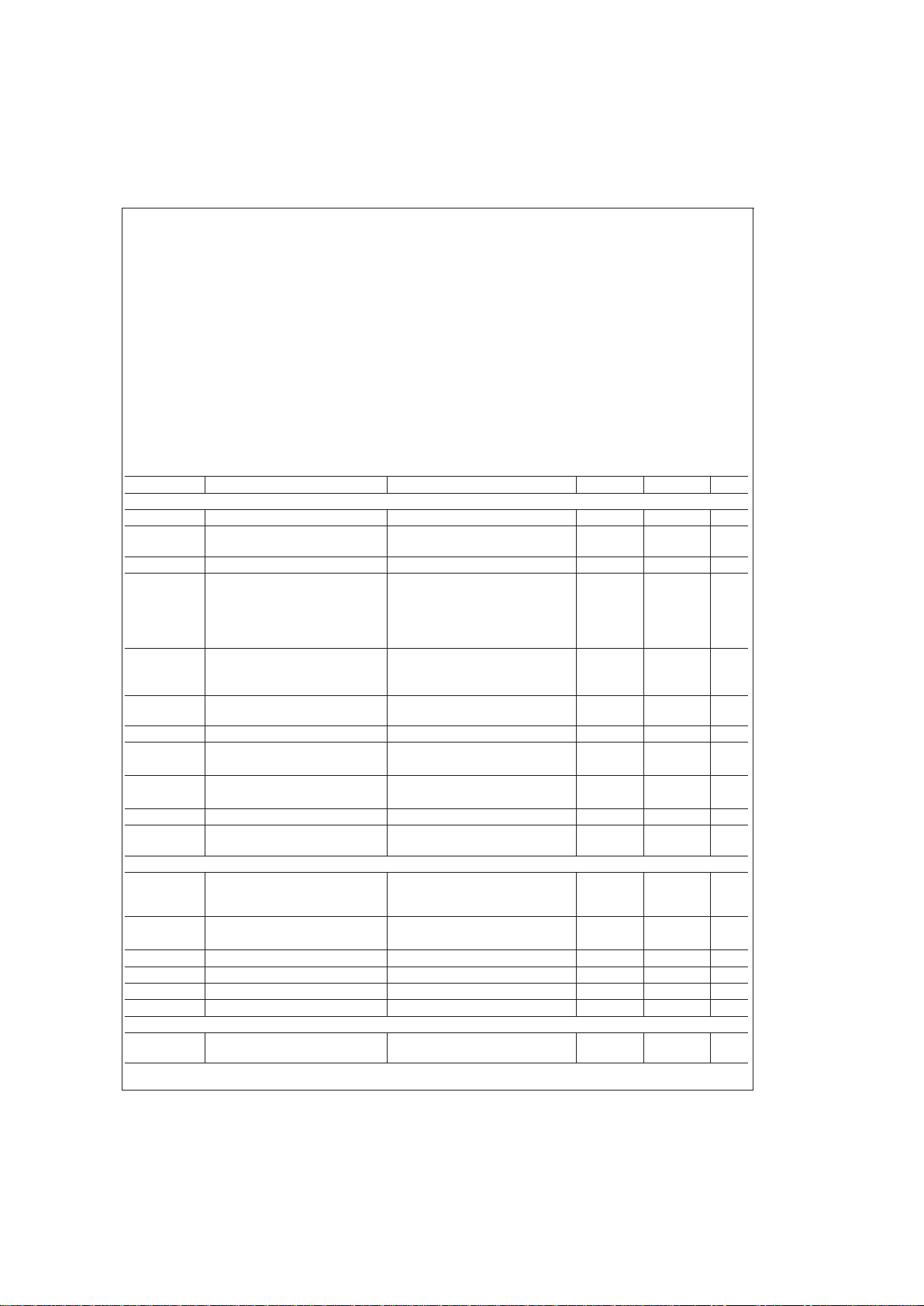
Absolute Maximum Ratings (Note 1)
Input Voltage
ON/OFF, Keep-Alive Inputs
(through 1 kΩ)
DC Input Voltage −26V to +26V
Positive Input Transient (t
<
100 ms) 60V
Negative Input Transient (t
<
1 ms) −50V
Reset Output Sink Current 5 mA
Power Dissipation Internally Limited
Junction Temperature 150˚C
ESD Susceptibility (Note 2) 12 kV, 2 kV
Lead Temperature
(Soldering, 10 seconds) 260˚C
Storage Temperature −50˚C to +150˚C
Operating Ratings (Note 1)
Input Voltage 6V to 26V
Ambient Temperature −40˚C to +125˚C
θjc, TO-220, TO-263 Packages 3˚C/W
θja, TO-220, TO-263 Packages 43˚C/W
θj-pins, SO20 Package 25˚C/W
θja, SO20 Package 85˚C/W
Electrical Characteristics
The following specifications apply for V
CC
=
6V to 26V, −40˚C ≤ T
A
≤ 125˚C, unless otherwise specified. C
OUT
=
47 µFd with an
ESR
<
3Ω.C
IN
=
1 µFd.
Symbol Parameter Conditions Min Max Units
REGULATOR OUTPUT
V
OUT
Output Voltage 5 mA ≤ I
OUT
≤ 250 mA 4.85 5.15 V
∆V
OUT
Line Line Regulation I
OUT
=
5 mA, 9V ≤ V
IN
≤ 16.5V
I
OUT
=
5 mA, 6V ≤ V
IN
≤ 26V
25
50
mV
mV
∆V
OUT
Load Load Regulation V
IN
=
14.4V, 5 mA ≤ I
OUT
≤ 250 mA 50 mV
Iq Quiescent Current V
ON/OFF
≤ V
IN
I
OUT
=
5mA
I
OUT
=
250 mA, V
IN
≥ 8V
I
OUT
=
5 mA, V
IN
=
5V
I
OUT
=
250 mA, V
IN
=
6V
4
25
10
50
mA
mA
mA
mA
Ioff OFF Quiescent Current V
IN
≤ 16.5V, Regulator OFF
−40˚C ≤ T
J
≤ 60˚C
60˚C ≤ T
J
≤ 135˚C
20
60
µA
µA
Vdo Dropout Voltage I
OUT
=
5mA
I
OUT
=
250 mA
300
800
mV
mV
Isc Short Circuit Current R
L
=
1Ω 0.4 1.5 A
RR Ripple Rejection fripple=120 Hz, Vripple=1 Vrms
I
OUT
=
50 mA 60 dB
Voth
OFF
Safety V
OUT
Latch-OFF Threshold In Keep-Alive mode
V
ON/OFF
=
0V, V
KA
=
0V 4 4.5 V
OVthr Overvoltage Shutdown Threshold 27 V
Vo Transient V
OUT
during Transients VINPeak ≤ 60V,
R
L
=
100Ω, τ=100 ms
7V
RESET OUTPUT
Vth Threshold Voltage ∆V
OUT
Required to Generate a
Reset Output
4.85V ≤ V
OUT
≤ 5.15V
−300 −500 mV
Vlow Reset Output Low Voltage Isink=1.6 mA, V
OUT
>
3.2V 0.4 V
1.4V ≤ V
OUT
≤ 3.2V 0.8 V
Vhigh Reset Output High Voltage 0.9 V
OUT
V
OUT
V
t
delay
Delay Time Cdelay=0.1 µFd 7 31 ms
I
delay
Charging Current for Cdelay 10 30 µA
Rpu Internal Pull-up Resistance 12 80 kΩ
CONTROL LOGIC
V
KA
low Low Input Threshold Voltage,
Keep-Alive Input
3.5V ≤ V
OUT
≤ 5.25V 0.3 V
OUT
0.5 V
OUT
V
LM9070
www.national.com3
Electrical Characteristics (Continued)
The following specifications apply for V
CC
=
6V to 26V, −40˚C ≤ T
A
≤ 125˚C, unless otherwise specified. C
OUT
=
47 µFd with an
ESR
<
3Ω.C
IN
=
1 µFd.
Symbol Parameter Conditions Min Max Units
CONTROL LOGIC
V
KA
high High Input Threshold Voltage,
Keep-Alive Input
3.5V ≤ V
OUT
≤ 5.25V 0.6 V
OUT
0.8 V
OUT
V
V
ON/OFF
low Low Input Voltage, ON/OFF Input Rseries=1kΩ −2 2 V
V
ON/OFF
high High Input Voltage, ON/OFF Input Rseries=1kΩ 426V
I
ON/OFF
Input Current, ON/OFF Input V
ON/OFF
≤ 4V 330 µA
4V
<
V
ON/OFF
<
7V 670 µA
V
ON/OFF
≥ 7V 10 mA
Rpu
KA
Internal Pull-up Resistance,
Keep-Alive Input
0V ≤ VIN≤ 26V
20 100 kΩ
Rpd
ON/OFF
Internal Pull-down Resistance
ON/OFF Input
0V ≤ V
ON/OFF
≤ 26V
50 210 kΩ
Note 1: Absolute Maximum Ratings indicate limits beyond which damage to the device may occur. Operating Ratings indicate conditions for which the device is
intended to be functional, but do not guarantee specific performance limits. For guaranteed specifications and conditions, see the Electrical Characteristics.
Note 2: All pins will survive an ESD impulse of
±
2000V using the human body model of 100 pF discharged through a 1.5 kΩ resistor. In addition, input pins VINand
the ON/OFF input will withstand ten pulses of
±
12 kV from a 150 pF capacitor discharged through a 560Ω resistor with each pin bypassed with a 22 nF, 100V ca-
pacitor.
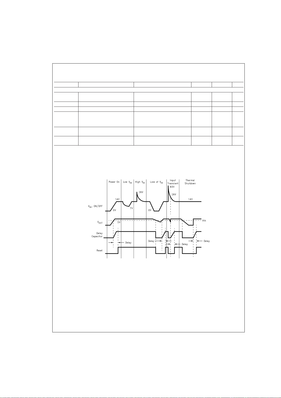
Reset Operation and Protection Features
DS012831-5
LM9070
www.national.com 4
 Loading...