

NSC LM9061MX, LM9061M Datasheet
TL/H/12317
LM9061 Power MOSFET Driver with Lossless Protection
April 1995
LM9061
Power MOSFET Driver with Lossless Protection
General Description
The LM9061 is a charge-pump device which provides the
gate drive to any size external power MOSFET configured
as a high side driver or switch. A CMOS logic compatible
ON/OFF input controls the output gate drive voltage. In the
ON state, the charge pump voltage, which is well above the
available V
CC
supply, is directly applied to the gate of the
MOSFET. A built-in 15V zener clamps the maximum gate to
source voltage of the MOSFET. When commanded OFF a
110 mA current sink discharges the gate capacitances of
the MOSFET for a gradual turn-OFF characteristic to minimize the duration of inductive load transient voltages and
further protect the power MOSFET.
Lossless protection of the power MOSFET is a key feature
of the LM9061. The voltage drop (V
DS
) across the power
device is continually monitored and compared against an
externally programmable threshold voltage. A small current
sensing resistor in series with the load, which causes a loss
of available energy, is not required for the protection circuitry. Should the V
DS
voltage, due to excessive load current,
exceed the threshold voltage, the output is latched OFF in a
more gradual fashion (through a 10 mA output current sink)
after a programmable delay time interval.
Designed for the automotive application environment the
LM9061 has a wide operating temperature range of
b
40§C
to
a
125§C, remains operational with VCCup to 26V, and
can withstand 60V power supply transients. The LM9061 is
available in an 8-pin small outline package, and an 8-pin
dual in-line package.
Features
Y
Built-in charge pump for gate overdrive of high side
drive applications
Y
Lossless protection of the power MOSFET
Y
Programmable MOSFET protection voltage
Y
Programmable delay of protection latch-OFF
Y
Fast turn-ON (1.5 ms max with gate capacitance of
25000 pF)
Y
Undervoltage shut OFF with V
CC
k
7V
Y
Overvoltage shut OFF with V
CC
l
26V
Y
Withstands 60V supply transients
Y
CMOS logic compatible ON/OFF control input
Y
Surface mount and dual in-line packages available
Applications
Y
Valve, relay and solenoid drivers
Y
Lamp drivers
Y
DC motor PWM drivers
Y
Logic controlled power supply distribution switch
Y
Electronic circuit breaker
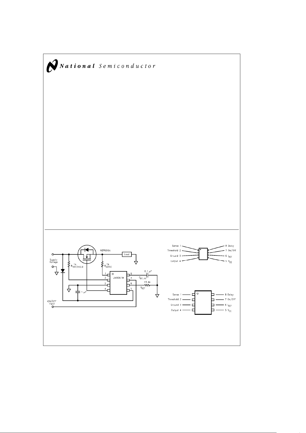
Typical Application
TL/H/12317– 1
Connection Diagrams
TL/H/12317– 3
Top View
Order Number LM9061M
See NS Package Number M08A
TL/H/12317– 2
Top View
Order Number LM9061N
See NS Package Number N08E
C
1995 National Semiconductor Corporation RRD-B30M115/Printed in U. S. A.
Absolute Maximum Ratings (Note 1)
If Military/Aerospace specified devices are required,
please contact the National Semiconductor Sales
Office/Distributors for availability and specifications.
Supply Voltage 60V
Reverse Supply Current 20 mA
Output Voltage V
CC
a
15V
Voltage at Sense and Threshold
(through 1 kX)
b
25V toa60V
ON/OFF Input Voltage
b
0.3V to V
CC
a
0.3V
Junction Temperature 150§C
Storage Temperature
b
55§Cto150§C
Lead Temperature (Soldering, 10 seconds) 260
§
C
Operating Ratings (Note 2)
Supply Voltage 7V to 26V
ON/OFF Input Voltage
b
0.3V to V
CC
Ambient Temperature Range
b
40§Cto125§C
Thermal Resistance (i
J-A
)
LM9061M 150§C/W
LM9061N 100
§
C/W
DC Electrical Characteristics
7VsV
CC
s
20V, R
REF
e
15.4 kX,b40§CsT
J
s
a
125§C, unless otherwise specified.
Symbol Parameter Conditions Min Max Units
POWER SUPPLY
I
Q
Quiescent Supply Current ON/OFFe‘‘0’’ 5 mA
I
CC
Operating Supply Current ON/OFFe‘‘1’’,
C
LOAD
e
0.025 mF,
40 mA
Includes Turn-ON
Transient Output Current
ON/OFF CONTROL INPUT
VIN(0) ON/OFF Input Logic ‘‘0’’ V
OUT
e
OFF 1.5 V
VIN(1) ON/OFF Input Logic ‘‘1’’ V
OUT
e
ON 3.5 V
V
HYST
ON/OFF Input Hysteresis Peak to Peak 0.8 2 V
I
IN
ON/OFF Input Pull-Down Current VON/OFFe5V 50 250 mA
GATE DRIVE OUTPUT
V
OH
Charge Pump Output Voltage ON/OFFe‘‘1’’ V
CC
a
7V
CC
a
15 V
V
OL
OFF Output Voltage ON/OFFe‘‘0’’,
0.9 V
I
SINK
e
110 mA
V
CLAMP
Sense to Output ON/OFFe‘‘1’’,
11 15 V
Clamp Voltage V
SENSE
e
V
THRESHOLD
I
SINK(Normal-OFF)
Output Sink Current, ON/OFFe‘‘0’’,
Normal Operation V
DELAY
e
0V, 75 145 mA
V
SENSE
e
V
THRESHOLD
I
SINK(Latch-OFF)
Output Sink Current with V
DELAY
e
7V,
515mA
Protection Comparator Tripped V
SENSE
k
V
THRESHOLD
PROTECTION CIRCUITRY
I
REF
Threshold Pin Reference Current V
SENSE
e
V
THRESHOLD
75 88 m A
V
REF
Reference Voltage 1.15 1.35 V
I
THR(LEAKAGE)
Threshold Pin Leakage Current V
CC
e
Open,
10 mA
7V
s
V
THRESHOLD
s
20V
I
SENSE
Sense Pin Input Bias Current V
SENSE
e
V
THRESHOLD
10 mA
DELAY TIMER
I
DELAY
Delay Pin Source Current 6.74 15.44 mA
V
TIMER
Delay Timer Threshold Voltage 5 6.2 V
I
DIS
Delay Capacitor Discharge Current V
DELAY
e
5V 2 10 mA
V
SAT
Discharge Transistor Saturation Voltage I
DIS
e
1 mA 0.4 V
2
AC Timing Characteristics
7VsV
CC
s
20V, R
REF
e
15.4 kX,b40§CsT
J
s
a
125§C, C
LOAD
e
0.025 mF, C
DELAY
e
0.022 mF, unless otherwise
specified.
Symbol Parameter Conditions Min Max Units
T
ON
Output Turn-ON Time C
LOAD
e
0.025 mF
7V
s
V
CC
s
10V, V
OUT
t
V
CC
a
7V 1.5 ms
10V
s
V
CC
s
20V, V
OUT
t
V
CC
a
11V 1.5 ms
T
OFF(Normal)
Output Turn-OFF Time, C
LOAD
e
0.025 mF
Normal Operation V
CC
e
14V, V
OUT
t
25V 4 10 ms
(Note 4) V
SENSE
e
V
THRESHOLD
T
OFF(Latch-OFF)
Output Turn-OFF Time, C
LOAD
e
0.025 mF
Protection Comparator Tripped V
CC
e
14V, V
OUT
t
25V 45 140 ms
(Note 4) V
SENSE
e
V
THRESHOLD
T
DELAY
Delay Timer Interval C
DELAY
e
0.022 mF 8 18 ms
Note 1: Absolute Maximum Ratings indicate the limits beyond which damage to the device may occur.
Note 2: Operating Ratings indicate conditions for which the device is intended to be functional, but may not meet the guaranteed specific performance limits. For
guaranteed specifications and test conditions see the Electrical Characteristics.
Note 3: ESD Human Body Model: 100 pF discharged through 1500X resistor.
Note 4: The AC Timing specifications for T
OFF
are not production tested, and therefore are not specifically guaranteed. Limits are provided for reference purposes
only. Smaller load capacitances will have proportionally faster turn-ON and turn-OFF times.
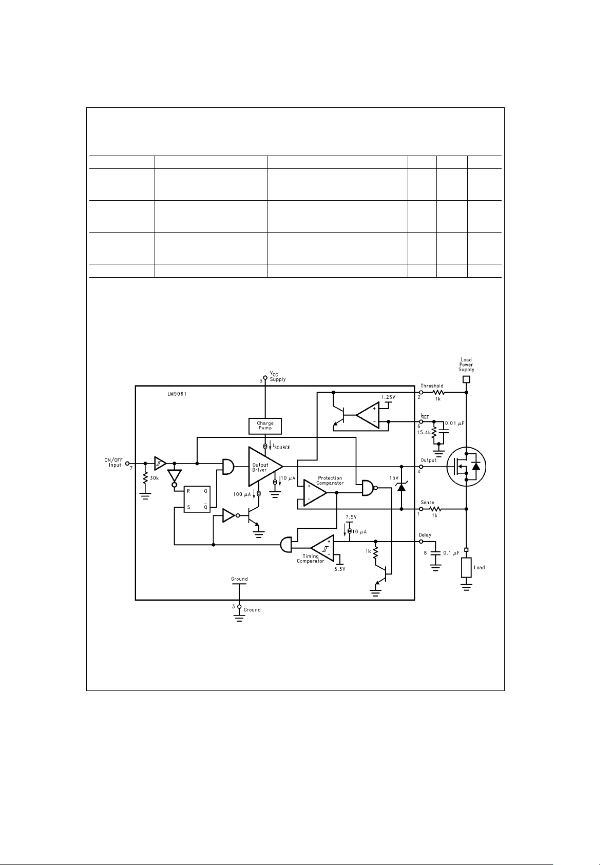
Block Diagram
TL/H/12317– 4
3
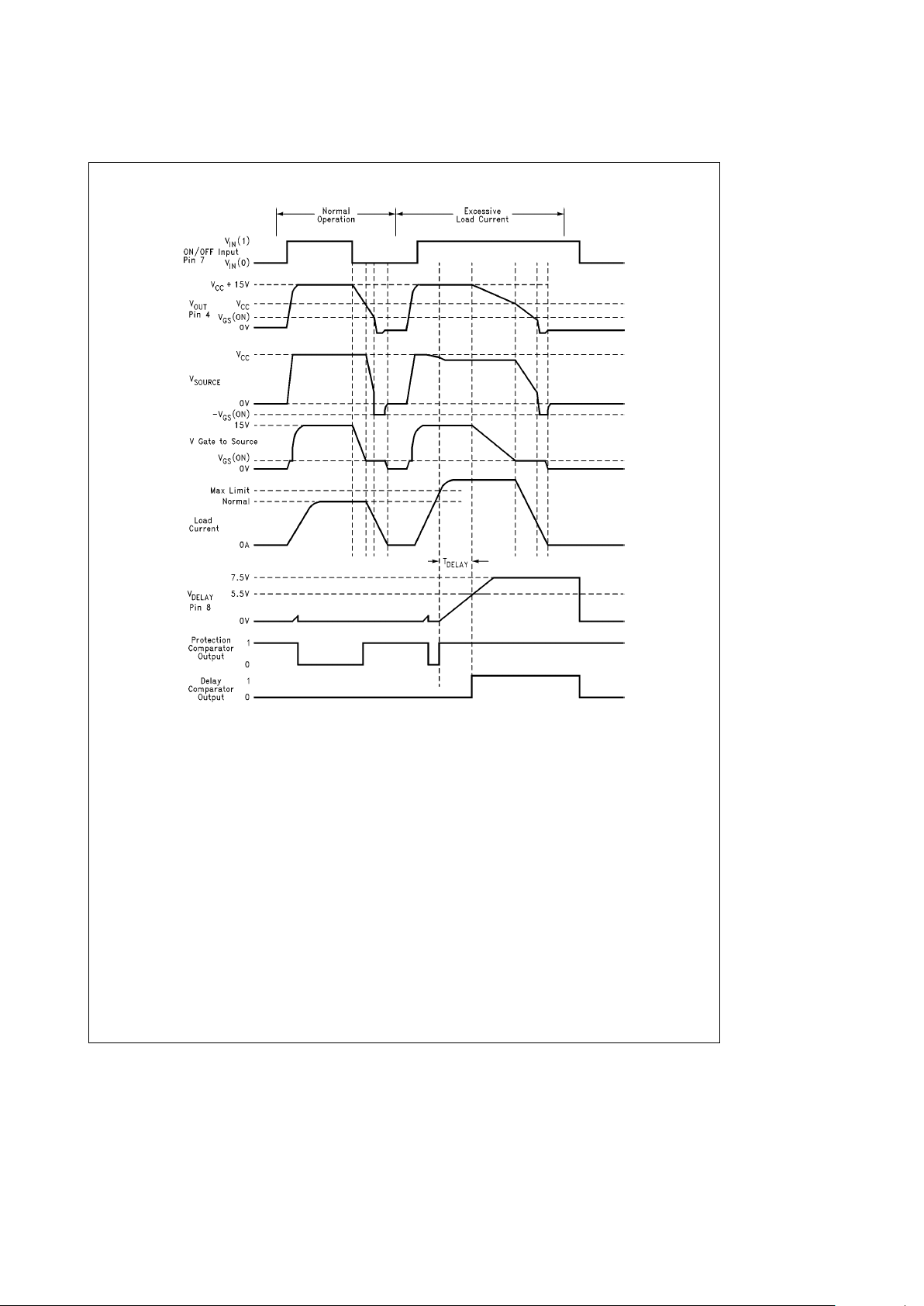
Typical Operating Waveforms
TL/H/12317– 5
4
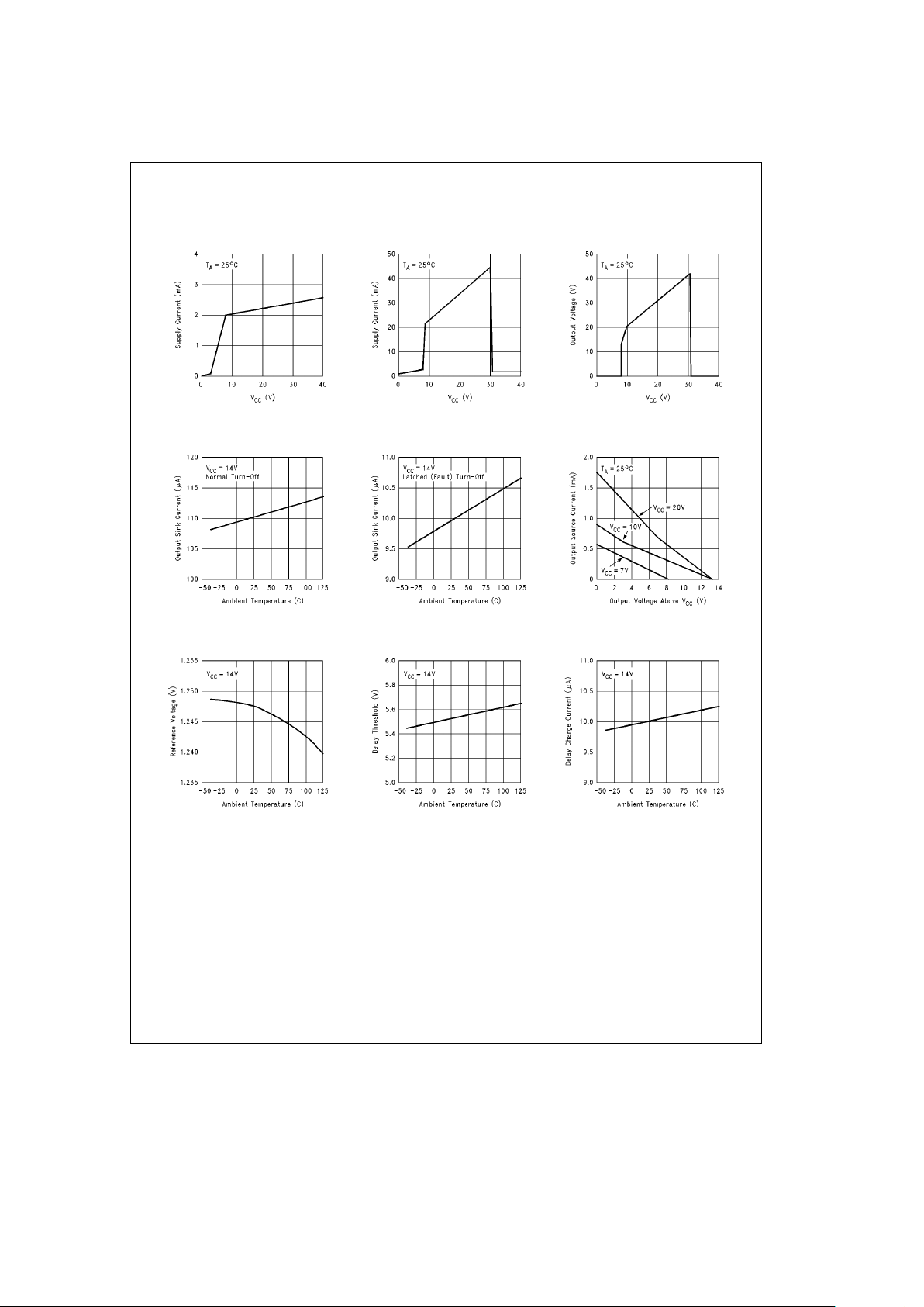
Typical Electrical Characteristics
vs V
CC
Standby Supply Current
vs V
CC
Operating Supply Current
vs V
CC
Output Voltage
vs Temperature
Output Sink Current
vs Temperature
Output Sink Current
vs Output Voltage
Output Source Current
vs Temperature
Reference Voltage
vs Temperature
Delay Threshold
vs Temperature
Delay Charge Current
TL/H/12317– 06
5
 Loading...