

NSC LM9040MX, LM9040M Datasheet
TL/H/12372
LM9040 Dual Lambda Sensor Interface Amplifier
August 1995
LM9040
Dual Lambda Sensor Interface Amplifier
General Description
The LM9040 is a dual sensor interface circuit consisting of
two independent sampled input differential amplifiers designed for use with conventional Lambda Oxygen Sensors.
The Lambda Sensor is used for monitoring the oxygen concentration in the exhaust of gasoline engines using catalytic
after treatment and will deliver a voltage signal which is dependent on the air-fuel mixture. The gain of the amplifiers
are internally set and can directly convert the Lambda sensor output voltage to a level suitable for A/D conversion in a
system using a 5V reference.
The input common mode voltage range of each amplifier is
g
2V with respect to the IC ground pin. This will allow the IC
to connect to sensors which are remotely grounded at the
engine exhaust manifold or exhaust pipe.
Each amplifier is capable of independent default operation
should either, or both, of the leads to a sensor become
open circuited.
Noise filtering is provided by an internal switched capacitor
low pass filter as part of each amplifier, and by external
components.
The LM9040 is fully specified over the automotive temperature range of
b
40§Ctoa125§C and is provided in a 14-pin
Small Outline surface mount package.
Features
Y
Single 5V supply operation
Y
Common mode input voltage range ofg2V
Y
Differential input voltage range of 50 mV to 950 mV
Y
Sampled differential input
Y
Switched capacitor low pass filter
Y
Internal oscillator and VBBgenerator
Y
Open input default operation
Y
Cold sensor default operation
Y
Low power consumption (42 mW max)
Y
Gain set by design and guaranteed over the operating
temperature range
Applications
Y
Closed loop emissions control
Y
Catalytic converter monitoring
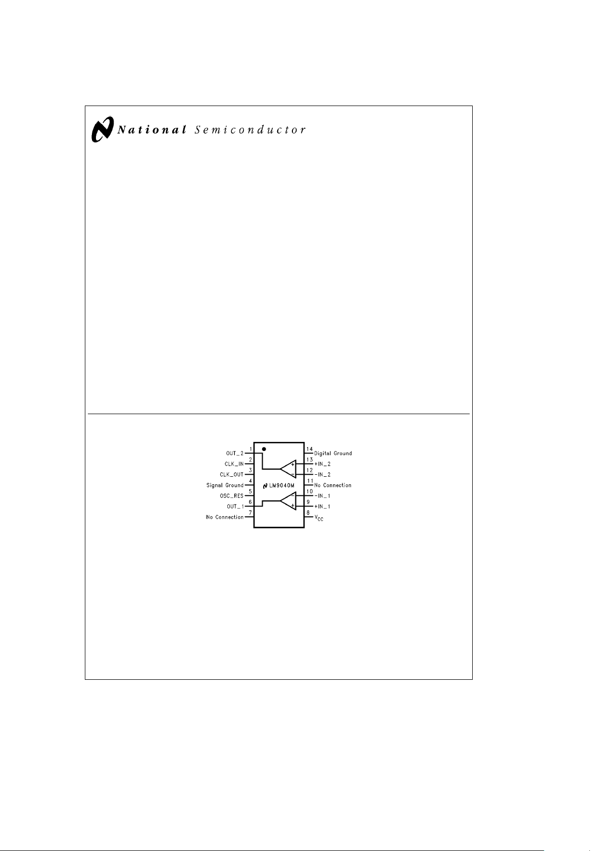
Connection Diagram
TL/H/12372– 1
Top View
Ordering Information
LM9040M
See NS Package Number M14B
C
1995 National Semiconductor Corporation RRD-B30M115/Printed in U. S. A.
Absolute Maximum Ratings
If Military/Aerospace specified devices are required,
please contact the National Semiconductor Sales
Office/Distributors for availability and specifications.
Supply Voltage
b
0.3V toa6.0V
Input Voltage Continuous (Note 1)
g
14V
Input Voltage Transient t
s
1 ms (Note 1)
g
60V
ESD Susceptibility (Note 2)
g
2000V
Maximum Junction Temperature 150§C
Storage Temperature Range
b
65§Ctoa150§C
Lead Soldering Information
Vapor Phase (60 Seconds) 215
§
C
Infrared (15 Seconds) 220
§
C
Operating Ratings
Supply Voltage 4.75V to 5.25V
Differential Input Voltage 0V toa1V
Common Mode Voltage
g
2V
Power Dissipation 42 mW
DC Electrical Characteristics
The following specifications apply for V
CC
e
5.0V, V
DIFF
e
500 mV, V
CM
e
0V, R
OSC
e
178 kX,b40§CsT
A
s
a
125§C, DC
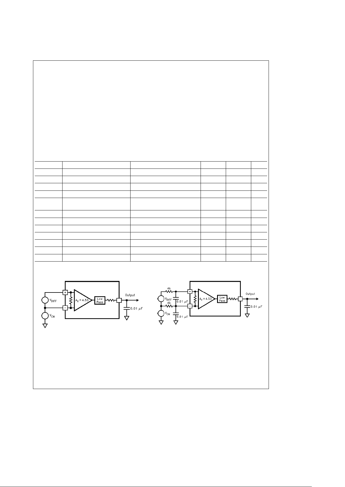
Test Circuit
Figure 1
, unless otherwise specified.
Symbol Parameter Conditions Min Max Units
I
CC
Supply Current 4.75VsV
CC
s
5.25V 8.0 mA
Z
DIFF
Differential Input Impedance 4.75VsV
CC
s
5.25V 1.05 1.60 Meg X
Z
IO
Inverting Input to Ground Impedance Non-Inverting Inputs Open 10.00 Meg X
V
OL
Output Low Voltage V
DIFF
e
0V, I
LOAD
e
2.0 mA 100 mV
V
OC
V
OUT
Center One, or Both, Input(s) Open V
CC
#
0.380 V
CC
#
0.425 V
4.75V
s
V
CC
s
5.25V
V
OUT(ERROR)(VOUT
)–(V
DIFF
#
4.53) 50 mVsV
DIFF
s
950 mV, V
CM
e
0V
g
65 mV
V
OH
Output High Voltage V
DIFF
e
5V, I
LOAD
eb
2mAV
CC
b
0.1V V
R
OUT
Output Resistance 1500 3500 X
CMRR
(DC)
DC Common Mode Error
b
2VsV
CM
s
a
2V
g
4.5 mV/V
T
RISE
Output Rise Time C
OUT
e
0.01 mF 1.2 ms
T
FALL
Output Fall Time C
OUT
e
0.01 mF 1.2 ms
F
C
Low Pass Filterb3dB C
OUT
e
0.01 mF 400 700 Hz
Note 1: The input voltage must be applied through external 4 kX input resistors. See
Figure 2
, AC Test Circuit. Amplifier operation will be disrupted, but will not be
destructive.
Note 2: ESD rating is with Human Body Model: 100 pF discharged through a 1500X resistor.
TL/H/12372– 2
FIGURE 1. DC Test Circuit
TL/H/12372– 3
FIGURE 2. AC Test Circuit
2
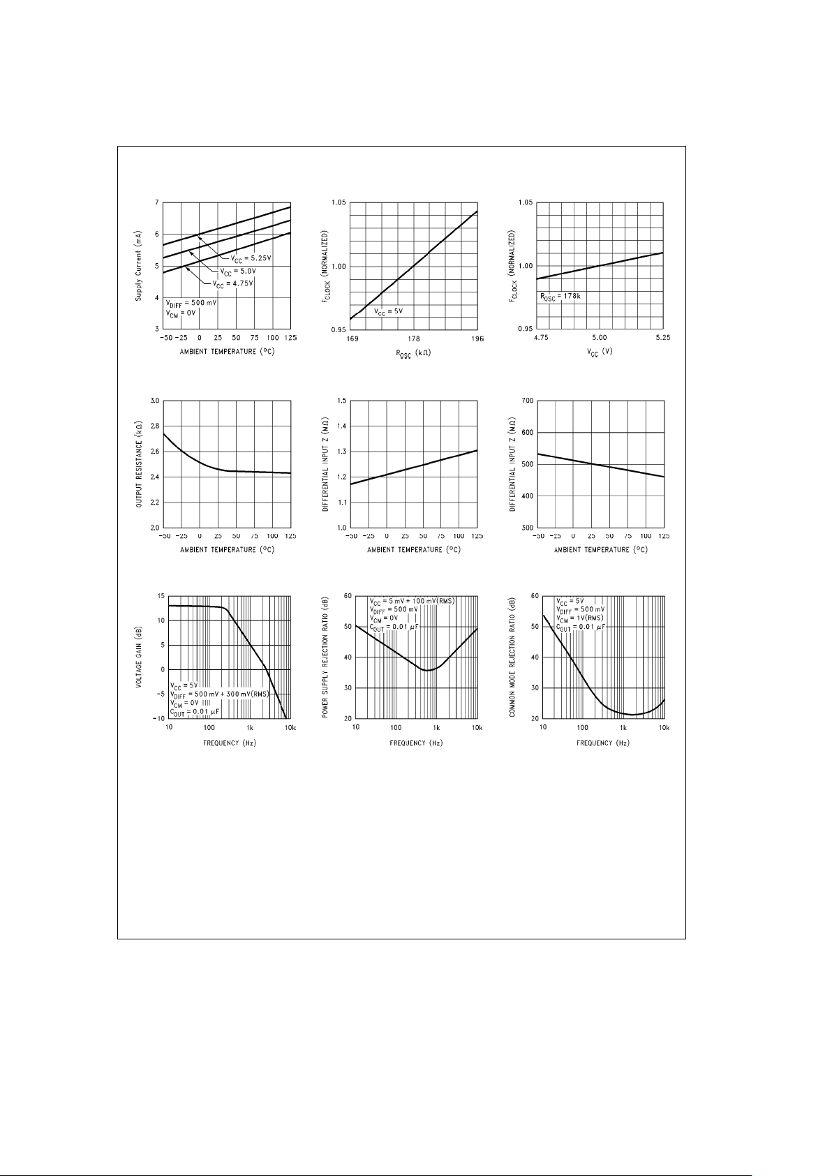
Typical Performance Characteristics
Supply Current vs Temperature
TL/H/12372– 4
F
CLOCK
(Normalized) vs R
OSC
TL/H/12372– 5
F
CLOCK
(Normalized) vs V
CC
TL/H/12372– 6
Output R vs Temperature
TL/H/12372– 7
Z
DIFF
vs Temperature
TL/H/12372– 8
FCvs Temperature
TL/H/12372– 9
Voltage Gain vs Frequency
TL/H/12372– 10
PSRR vs Frequency
TL/H/12372– 11
CMRR vs Frequency
TL/H/12372– 12
3
 Loading...