NSC LM9022MX, LM9022M Datasheet

LM9022
Vacuum Fluorescent Display Filament Driver
General Description
The LM9022 is a bridged power amplifier capable of delivering typically 2W of continuous average power into a 10Ω
filament load when powered by a 5V power supply.
To conserve power in portable applications, the LM9022’s
micropower shutdown mode (I
Q
= 0.6µA, typ) is activated
when V
DD
is applied to the SHUTDOWN pin.
Additional LM9022 features include thermal shutdown protection, unity-gain stability, and external gain set.
Key Specifications
n IDDduring shutdown 0.6µA (typ)
n Thermal Shutdown Protection
Features
n No transformers required
n SO or DIP packaging
Applications
n VCR/DVD Displays
n RADIO/TUNER Displays
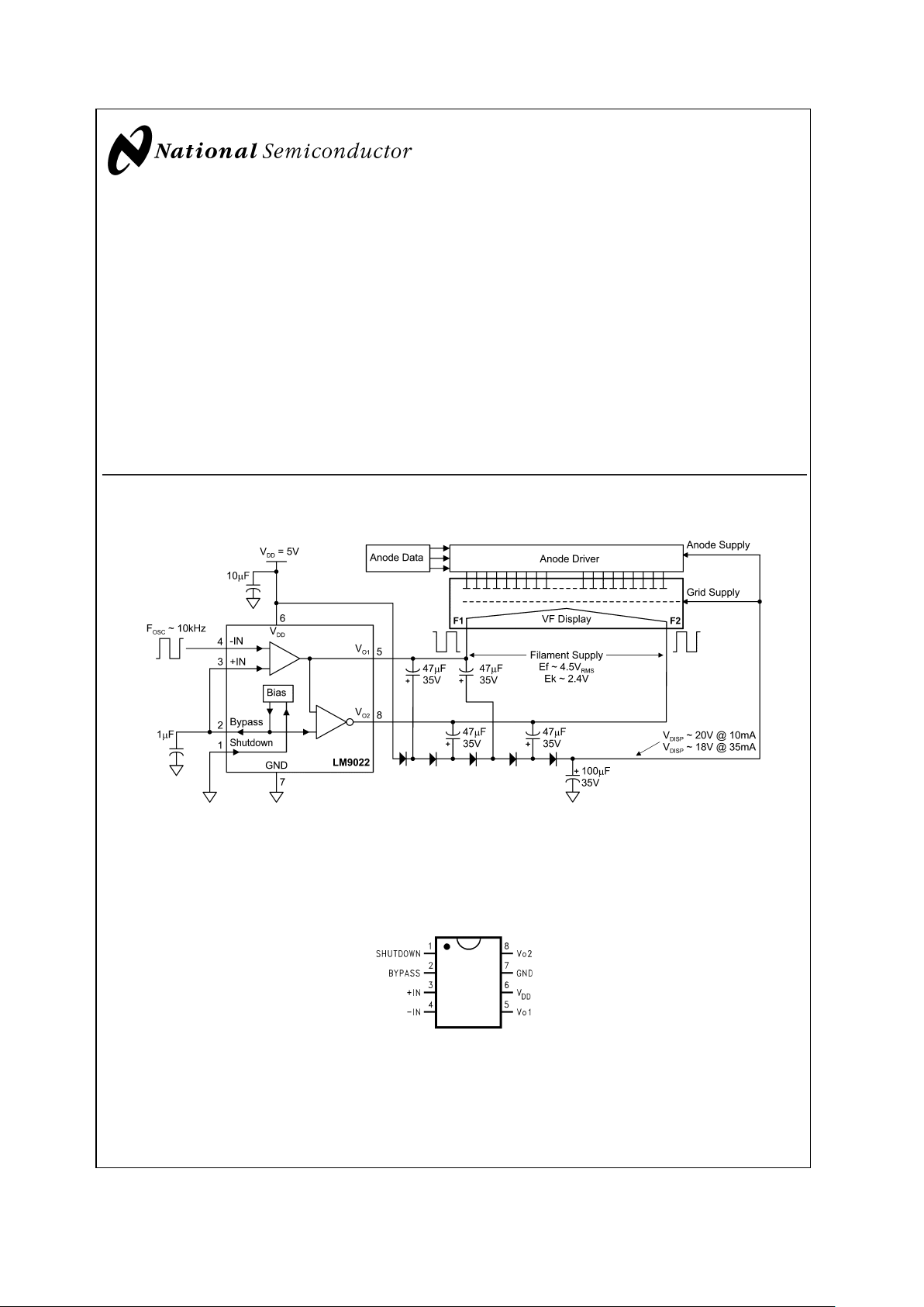
Typical Application T
A
= 25˚C, VDD= 5V, unless otherwise specified.
Connection Diagram
MSOP, Small Outline, and DIP Package
20021502
Top View
Order Number LM9022M or LM9022N
See NS Package Number M08A or N08E
20021501
FIGURE 1. Typical Application Circuit
July 2002
LM9022 Vacuum Fluorescent Display Filament Driver
© 2002 National Semiconductor Corporation DS200215 www.national.com

Absolute Maximum Ratings (Note 1)
If Military/Aerospace specified devices are required,
please contact the National Semiconductor Sales Office/
Distributors for availability and specifications.
Supply Voltage -0.3V to +6.0V
Supply Temperature −65˚C to +150˚C
Input Voltage −0.3V to V
DD
+0.3V
Power Dissipation (Note 3) Internally Limited
ESD Susceptibility (Note 4) 5000V
ESD Susceptibility (Note 5) 250V
Junction Temperature 150˚C
Soldering Information
Small Outline Package
Vapor Phase (60 sec.) 215˚C
Infrared (15 sec.) 220˚C
See AN-450 ’Surface Mounting and their Effects on
Product Reliability’ for other methods of
soldering surface mount devices.
θ
JC
(typ) —M08A 35˚C/W
θ
JA
(typ) — M08A 140˚C/W
θ
JC
(typ) — N08E 37˚C/W
θ
JA
(typ) — N08E 107˚C/W
Operating Ratings
Temperature Range
T
MIN
≤ TA≤ T
MAX
−40˚C ≤ TA≤ 85˚C
Supply Voltage 2.0V ≤ V
DD
≤ 5.5V
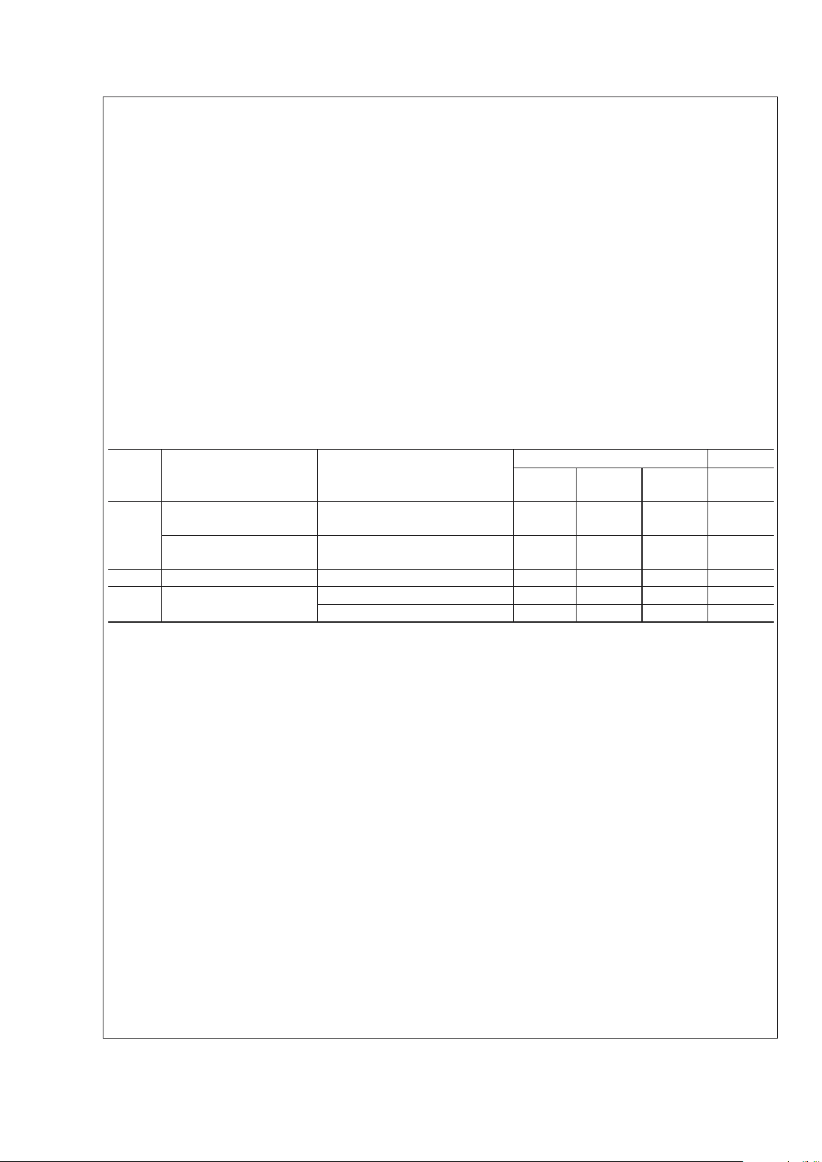
Electrical Characteristics (Notes 1, 2)
The following specifications apply for V
DD
= 5V, V
PIN3=VPIN2,VSHUTDOWN
= 0V, and RL=10Ω unless otherwise specified.
Limits apply for T
A
= 25˚C.
Symbol Parameter Conditions
LM9022
Min
(Note 7)
Typical
(Note 6)
Max
(Note 7)
Units
I
DD
Quiescent Power Supply
Current
VIN= 0V, Io= 0A, V
SHUTDOWN
= 0V 6.5 10.0 mA
Power Supply Current during
shutdown
V
SHUTDOWN
=VDD(Note 8) 0.6 2 µA
V
BP
Bypass Pin Voltage VIN= 0V 2.4 2.5 2.6 V
V
OUT
Output Voltage Across R
L
RL=10Ω 3.6 4.3 V
R
L
=20Ω 4.2 4.6 V
Note 1: Absolute Maximum Ratings indicate limits beyond which damage to the device may occur. Operating Ratings indicate conditions for which the device is
functional, but do not guarantee specific performance limits. Electrical Characteristics state DC and AC electrical specifications under particular test conditions which
guarantee specific performance limits. This assumes that the device is within the Operating Ratings. Specifications are not guaranteed for parameters where no limit
is given, however, the typical value is a good indication of device performance.
Note 2: All voltages are measured with respect to the ground pin, unless otherwise specified.
Note 3: The maximum power dissipation must be derated at elevated temperatures and is dictated by T
JMAX
, θJA, and the ambient temperature TA. The maximum
allowable power dissipation is P
DMAX
=(T
JMAX–TA
)/θJAor the number given in Absolute Maximum Ratings, whichever is lower. For the LM9022, T
JMAX
= 150˚C.
For the θ
JA
’s for different packages, please see the Application Information section or the Absolute Maximum Ratings section.
Note 4: Human body model, 100pF discharged through a 1.5kΩ resistor.
Note 5: Machine Model, 220pF–240pF discharged through all pins.
Note 6: Typicals are specified at 25˚C and represent the parametric norm.
Note 7: Limits are guaranteed to National’s AOQL (Average Outgoing Quality Level) by design, test, or statistical analysis.
Note 8: Both outputs are high impedance when in shutdown mode.
LM9022
www.national.com 2

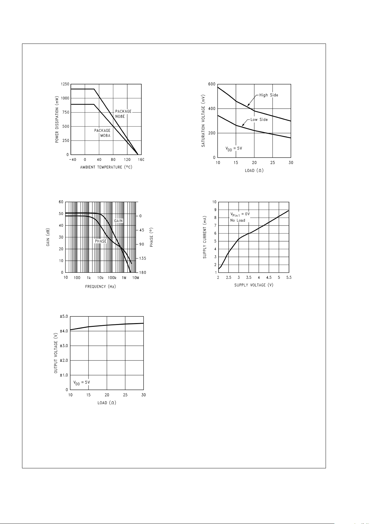
Typical Performance Characteristics
TA= 25˚C, VDD= 5V, unless otherwise specified.
Power Derating Curve Output Saturation Voltage
vs Load
20021514
20021515
Open Loop
Frequency Response
Supply Current
vs Supply Voltage
20021519
20021520
Differential Output Voltage
vs Load
20021540
LM9022
www.national.com3
 Loading...