

NSC LM9011MX, LM9011M Datasheet
LM9011
Electronic Ignition Interface
General Description
The LM9011 is an interface circuit which integrates the timing detection and logic control functions required for an automotive electronic ignition system into one device.
A VRS interface is provided for crankshaft position information via a toothed-wheel.
Four voltage comparators are provided for hardware diagnostics.
An electronic timing interface with output fault diagnostics is
provided to enable a micro-processor to drive an external
four channel ignition spark circuit.
The LM9011 is fully specified over the automotive temperature range of -40˚C to +125˚C, and is available in a 28 pin
Small Outline surface mount package.
Key Specifications
Features
n Single 5V supply operation
n VR Sensor Interface with dynamic hysteresis
n Four Channel Electronic Timing spark driver with output
diagnostics
n Electronic Timing Interface spark driver output voltage
from 5V to 16V
n One Non-Inverting voltage comparator with hysteresis
n Three Inverting voltage comparators with hysteresis
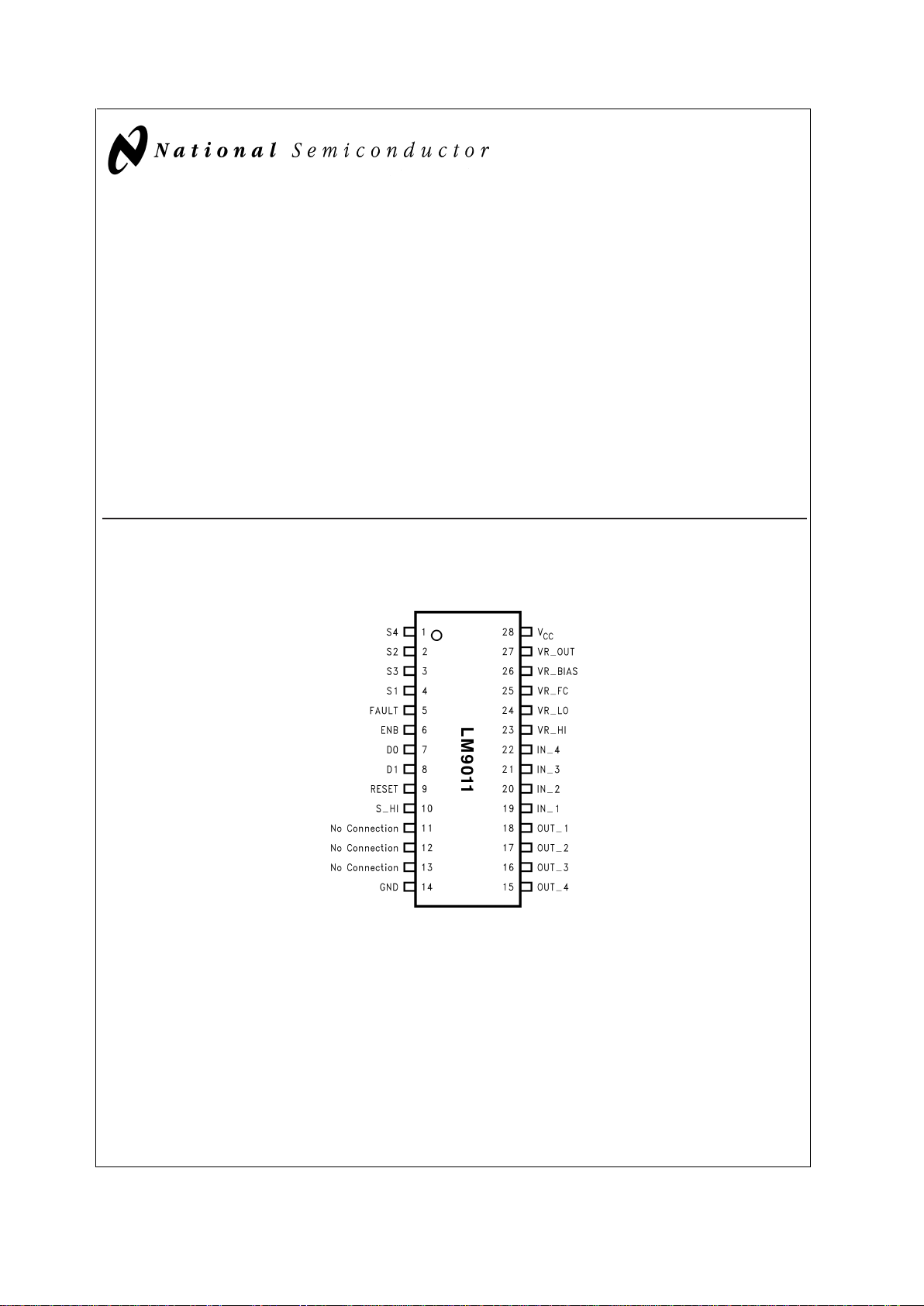
Connection Diagram
Top View
DS101264-1
Ordering Information LM9011M
See NS Package M28B
February 2000
LM9011 Electronic Ignition Interface
© 2000 National Semiconductor Corporation DS101264 www.national.com
Absolute Maximum Ratings (Note 1)
Voltage -0.3V to +7.0V
S_HI Voltage -0.3V to 26.5V
VR_HI and VR_LO Inputs +/-3mA
Comparator Inputs -0.3V to +7.0V
Timing Interface Inputs -0.3V to +7.0V
ESD Susceptibility (Note 3) +/-2000V
Maximum Junction Temperature 150˚C
Storage Temperature Range -65˚C to +150˚C
Lead Soldering Information:
Vapor Phase (60 Seconds) 215˚C
Infrared (15 Seconds) 220˚C
Operating Ratings (Note 3)
V
CC
Voltage 4.75V to 5.25V
S_HI Voltage V
CC
to 26V
Sx Outputs -0.3V to S_HI +0.3V
Comparator Inputs
VR_HI and VR_LO Inputs
-0.3V to V
CC
+0.3V
+/-2.75mA
Timing Interface Inputs -0.3V to V
CC
+0.3V
Thermal Resistances (M28B):
Junction to Case (θJ-C) 15˚C/W
Junction to Ambient (θJ-C) 69˚C/W
DC Electrical Characteristics The following specifications apply for V
CC
= 5V, V
RESET=VCC,VS_HI
=
V
CC
, -40˚C ≤ TA≤ +125˚C, Application Circuit Figure 16, unless otherwise specified.
Symbol Parameter Conditions Minimum Maximum Units
I
CC
Supply Current
RESET, IN_4 = V
CC
25 mA
ENB, D0, D1, IN_1, IN_2, IN_3 =
0V
VR_HI = +12.5µA
VR_LO = -12.5µA
Comparators
V
TH
1 Input Threshold VIN_1 Decreasing from VCCto 0V
until V
OUT
_1>VCC/2
V
CC
X 0.435 VCCX 0.485 V
V
TH
2 Input Threshold VIN_2 Decreasing from VCCto 0V
until V
OUT
_2>VCC/2
V
CC
X 0.435 VCCX 0.485 V
V
TH
3 Input Threshold VIN_3 Decreasing from VCCto 0V
until V
OUT
_3>VCC/2
V
CC
X 0.40 VCCX 0.45 V
V
TH
4 Input Threshold VIN_4 Decreasing from VCCto 0V
until V
OUT
_4<VCC/2
V
CC
X 0.45 VCCX 0.50 V
V
HYST
Input Hysteresis All Comparators 150 400 mV
I
BIAS
Input Bias Current IN_1, IN_2, IN_3 = 0V ≤ VIN≤V
CC
IN_4 = 0V ≤ VIN_4 ≤ VCC-1V
750 µA
V
OH
Output High Voltage I
LOAD
= -100µAV VCC-1 V
V
OL
Output Low Voltage I
LOAD
= +100µAV 750 mV
VR Sensor Interface
V
OH
Output High Voltage I
LOAD
= -15µA
VR_HI= -1mA, VR_LO = +1mA
VCC-1 V
V
OL
Output Low Voltage Load = +15µA
VR_HI=+1mA, VR_LO = -1mA
750 mV
I
DIFF(MIN)
Minimum Detect Differential Input
Current (Note 4)
-40˚C ≤ TA≤ +25˚C
T
A
= +85˚C (Note 7)
T
A
= +125˚C
0.5
0.6
1.0
3.0
3.5
5.0
uA Pk-Pk
uA Pk-Pk
uA Pk-Pk
I
HYS
1 Input Hysteresis (Note 4) I
DIFF
= 1mA pk-pk 75 250 uA Pk
I
HYS
2 Input Hysteresis (Note 4) I
DIFF
= 2.5mA pk-pk 185 625 uA Pk
Electronic Timing Interface
V
IH
Input Logic 1 D0, D1, ENB,
RESET
VCCX 0.7 V
V
IL
Input Logic 0 D0, D1, ENB,
RESET
VCCX 0.3 V
I
IH
Input High Current Inputs D0, D1,
RESET
VIN=V
CC
10 µA
I
IH
Input High Current Input ENB VIN=V
CC
125 µA
LM9011
www.national.com 2
DC Electrical Characteristics The following specifications apply for V
CC
= 5V, V
RESET
=VCC,V
S_HI=VCC
,
-40˚C ≤ T
A
≤ +125˚C, Application Circuit Figure 16, unless otherwise specified. (Continued)
Symbol Parameter Conditions Minimum Maximum Units
Electronic Timing Interface
I
IL
Input Low Current Inputs D0, D1,
ENB
VIN= 0V -10 µA
I
IL
Input Low Current Input RESET VIN= 0V -125 µA
V
OH
Output High Voltage Outputs S1,
S2, S3, S4
I
LOAD
= -10mA, V
S_HI
= 5V 3.75 V
V
OL
Output Low Voltage Outputs S1,
S2, S3, S4
I
LOAD
= 1mA, V
S_ HI
= 5V 300 mV
V
OH
Output High Voltage Outputs S1,
S2, S3, S4
I
LOAD
= -10mA, V
S_HI
= 16V 14 V
V
OL
Output Low Voltage Outputs S1,
S2, S3, S4
I
LOAD
= 1mA, V
S_HI
=16V 450 mV
V
OH
Output High Voltage Outputs S1,
S2, S3, S4
I
LOAD
= -10mA, V
S_HI
=26V 22 V
V
OL
Output Low Voltage Outputs S1,
S2, S3, S4
I
LOAD
= 1mA, V
S_HI
=26V 600 mV
V
OH
FAULT Pin Output High Voltage I
FAULT
= -100µA, no fault VCC-1 V
V
OL
FAULT Pin Output Low Voltage I
FAULT
= 100µA, any fault 750 mV
V
FAULT
Fault Treshold Voltage Outputs
S1, S2, S3, S4
Sx Output Short Fault VCCX 0.2 VCCX 0.5 V
I
FOL
TRI-STATE Output Current
Outputs S1, S2, S3, S4
V
RESET
= 0V, V
S _HI
=5V
R
LOAD
= 10KΩ
-12 -50 µA
AC Electrical Characteristics
The following specifications apply for VCC= 5V, V
S_HI=VCC,VRESET=VCC
, -40˚C≤TA≤+125˚C. The AC Timing Characteristics
are not production tested. Minimum and Maximum limits are guaranteed by device characterization.
Symbol Parameter Conditions Minimum Maximum Units
Comparators
T
RISE
Output Rise Time 10%to 90%,C
LOAD
= 25pF 5 µs
T
FALL
Output Fall Time 90%to10%,C
LOAD
= 25pF 5 µs
VR Sensor Interface (Note 4)
T
RISE
Output Rise Time 10%to 90%,C
LOAD
= 100pF,
R
LOAD
= 100KΩ
10 µs
T
FALL
Output Fall Time 90%to10%,C
LOAD
= 100pF,
R
LOAD
= 100kΩ
5ms
T
DELAY
Zero Crossing Delay Time (Note6)I
DIFF
= 5µA pk-pk, F
VRS
= 200Hz
I
DIFF
= 50µA pk-pk, F
VRS
=
2.5KHz
1
10
ms
ms
F
MAX
Maximum VRS Frequency C
LOAD
= 100pF, R
LOAD
= 100KΩ
I
DIFF
= 5µA pk-pk
50 KHz
Electronic Timing Interface
T
RISE
1 Sx Output Rise Time Sx Rises10%to 90
%
C
LOAD
= 6.8nF, R
LOAD
= 10KΩ 5µs
C
LOAD
= 12.7nF, R
LOAD
= 10KΩ 8µs
T
FALL
1 Sx Output Fall Time Sx Falls 90%to 10
%
C
LOAD
= 6.8nF, R
LOAD
= 10KΩ 15 µs
C
LOAD
= 12.7nF, R
LOAD
= 10KΩ 25 µs
T
SETUP
SetupTime (Notes 7, 8 and 9) 1 µs
T
HOLD
Hold Time 0.5 µs
LM9011
www.national.com3
AC Electrical Characteristics (Continued)
The following specifications apply for VCC= 5V, V
S_HI=VCC,VRESET=VCC
, -40˚C≤TA≤+125˚C. The AC Timing Characteristics
are not production tested. Minimum and Maximum limits are guaranteed by device characterization.
Symbol Parameter Conditions Minimum Maximum Units
Electronic Timing Interface
T
DF
1 Fault Delay Time Sx Output Short to Ground Fault
From ENB=1toFAULT ≤ 10
%
C
FAULT
= 25pF 2 µs
T
DF
2 Fault Delay Time Sx Output Short to Battery Fault
From ENB=0toFAULT ≤ 10
%
C
FAULT
= 25pF 2 µs
T
TRI
TRI-STATE Delay Time From RESET=0toAllSx
Outputs Off
2µs
T
RISE
2 Fault Pin Rise Time 10%to 90%,C
FAULT
= 25pF 5 µs
T
FF(OFF)
False Fault Time From ENB=0toFAULT ≥ 90
%
C
FAULT
= 25pF
C
LOAD
= 6.8nF, R
LOAD
= 10KΩ 25 µs
C
LOAD
= 12.7nF, R
LOAD
= 10KΩ 30 µs
T
FF(ON)
False Fault Time From ENB=1toFAULT ≥ 90
%
C
FAULT
= 25pF
C
LOAD
= 6.8nF, R
LOAD
= 10KΩ 8µs
C
LOAD
= 12.7, R
LOAD
= 10KΩ 10 µs
T
UDF
Undefined Fault Time From ENB = 0 for 8uSec, to Valid
FAULT
C
LOAD
= 6.8nF, R
LOAD
= 10KΩ 20 µs
C
LOAD
= 12.7nF, R
LOAD
= 10KΩ 25 µs
Note 1: Absolute Maximum Ratings indicate the limits beyond which damage may occur.
Note 2: ESD Ratings is with Human Body Model: 100pF discharged through a 1500Ω resistor.
Note 3: Operating ratings indicateconditions for which the device is intended to be functional, but may not meet the guaranteed specificperformance limits. For guar-
anteed specifications and conditions, see the Electrical Characteristics.
Note 4: Tested per VR Sensor Interface test circuit. See figures 8 and 9.
Note 5: Minimum Detect Current is not production tested at +85C. Specifications is guaranteed through device characterization and Test Limits at 25˚C and 125˚C.
Note 6: VR Sensor Interface Tdelay, measured from VR input sine wave zero-crossing to VR_OUT going high. See figure 9.
Note 7: Electronic Timing Interface Tsetup, minimum time between Vcc
>
4.75V and RESET = 1.
Note 8: Electronic Timing Interface Tsetup, minimum time between RESET = 1 and D0 = 1.
Note 9: Electronic Timing Interface Tsetup, minimum time between D0 / D1 = valid and ENB = 1.
LM9011
www.national.com 4
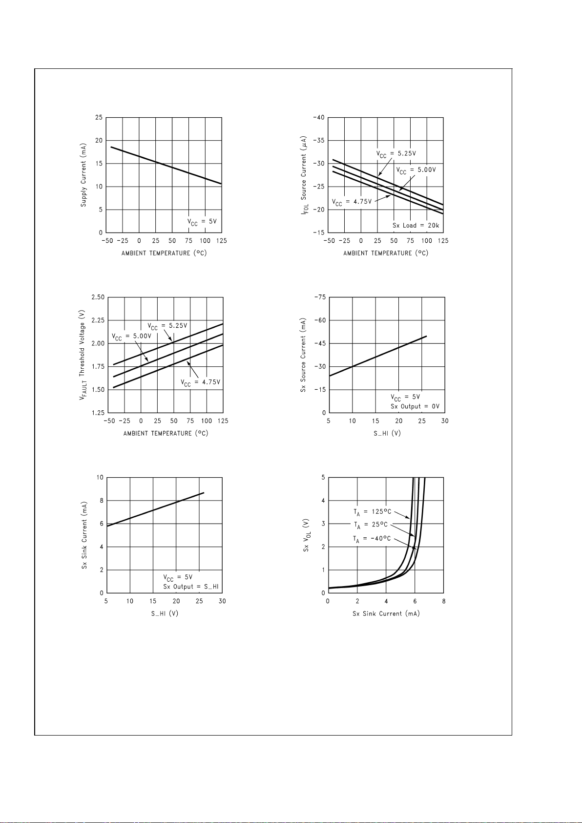
Typical Performance Characteristics
Supply Current vs Temperature
DS101264-3
Ifol Source Current vs Temperature
DS101264-4
VFault Threshold vs Temperature
DS101264-5
Sx Source Current vs S_HI Voltage
DS101264-6
Sx Sink Current vs S_HI Voltage
DS101264-7
Sx Vol vs Sx Sink Current
DS101264-8
LM9011
www.national.com5
 Loading...