

NSC LM87CIMT Datasheet
April 2000
LM87
Serial Interface System Hardware Monitor with Remote
Diode Temperature Sensing
LM87 Serial Interface System Hardware Monitor with Remote Diode Temperature Sensing
General Description
The LM87 is a highly integrated data acquisition system for
hardware monitoring of servers, Personal Computers, or virtually any microprocessor-based system. In a PC, the LM87
can be used to monitor power supply voltages, motherboard
and processor temperatures, and fan speeds. Actual values
for these inputs can be read at any time. Programmable
WATCHDOG
mable and maskable interrupt system with two outputs (INT
and THERM#).
The LM87 has an on-chip digital output temperature sensor
with 8-bit resolution as well as the capability of monitoring 2
external diode temperatures to 8-bit resolution, an 8 channel
analog input ADC with 8-bit resolution and an 8-bit DAC. A
channel on the ADC measures the supply voltage applied to
the LM87, nominally 3.3 V. Two of the ADC inputs can be redirected to a counter that can measure the speed of up to 2
fans. A slow speed Σ∆ ADC architecture allows stable measurement of signals in an extremely noisy environment. The
DAC, witha0to2.5Voutput voltage range, can be used for
fan speed control.Additional inputs are provided for Chassis
Intrusion detection circuits, and VID monitor inputs. The VID
monitor inputs can also be used as IRQ inputs if VID monitoring is not required. The LM87 has a Serial Bus interface
that is compatible with SMBus
™
limits in the LM87 activate a fully program-
™
and I2C™.
Features
n Remote diode temperature sensing (2 channels)
n 8 positive voltage inputs with scaling resistors for
monitoring +5 V, +12 V, +3.3 V, +2.5 V, Vccp power
supplies directly
n 2 inputs selectable for fan speed or voltage monitoring
n 8-bit DAC output for controlling fan speed
n Chassis Intrusion Detector input
™
n WATCHDOG
n SMBus or I
n VID0-VID4 or IRQ0-IRQ4 monitoring inputs
n On chip temperature sensor
#
Key Specifications
n Voltage Monitoring Error
n External Temperature Error
n Internal Temperature Error
−40 ˚C to +125 ˚C
n Supply Voltage Range 2.8 to 3.8 V
n Supply Current 0.7 mA (typ)
n ADC and DAC Resolution 8 Bits
n Temperature Resolution 1.0 ˚C
comparison of all monitored values
2
C Serial Bus interface compatibility
Applications
n System Thermal and Hardware Monitoring for Servers,
Workstations and PCs
n Networking and Telecom Equipment
n Office Electronics
n Electronic Test Equipment and Instrumentation
±
2 % (max)
±
4 ˚C (max)
±
3 ˚C (typ)
Ordering Information
Temperature Range
−40 ˚C ≤ T
Order Number Device Marking
LM87CIMT
LM87CIMTX
Note:1-Rail transport media, 61 parts per rail
2
-Tape and reel transport media, 2500 parts per reel
TRI-STATE®is a registered trademark of National Semiconductor Corporation.
WATCHDOG
SMBus
© 2000 National Semiconductor Corporation DS100995 www.national.com
™
is a trademark of National Semiconductor Corporation.
™
is a trademark of the Intel Corporation.
1
2
≤ +125 ˚C
A
LM87CIMT MTC24B
LM87CIMT MTC24B
NS Package
Number
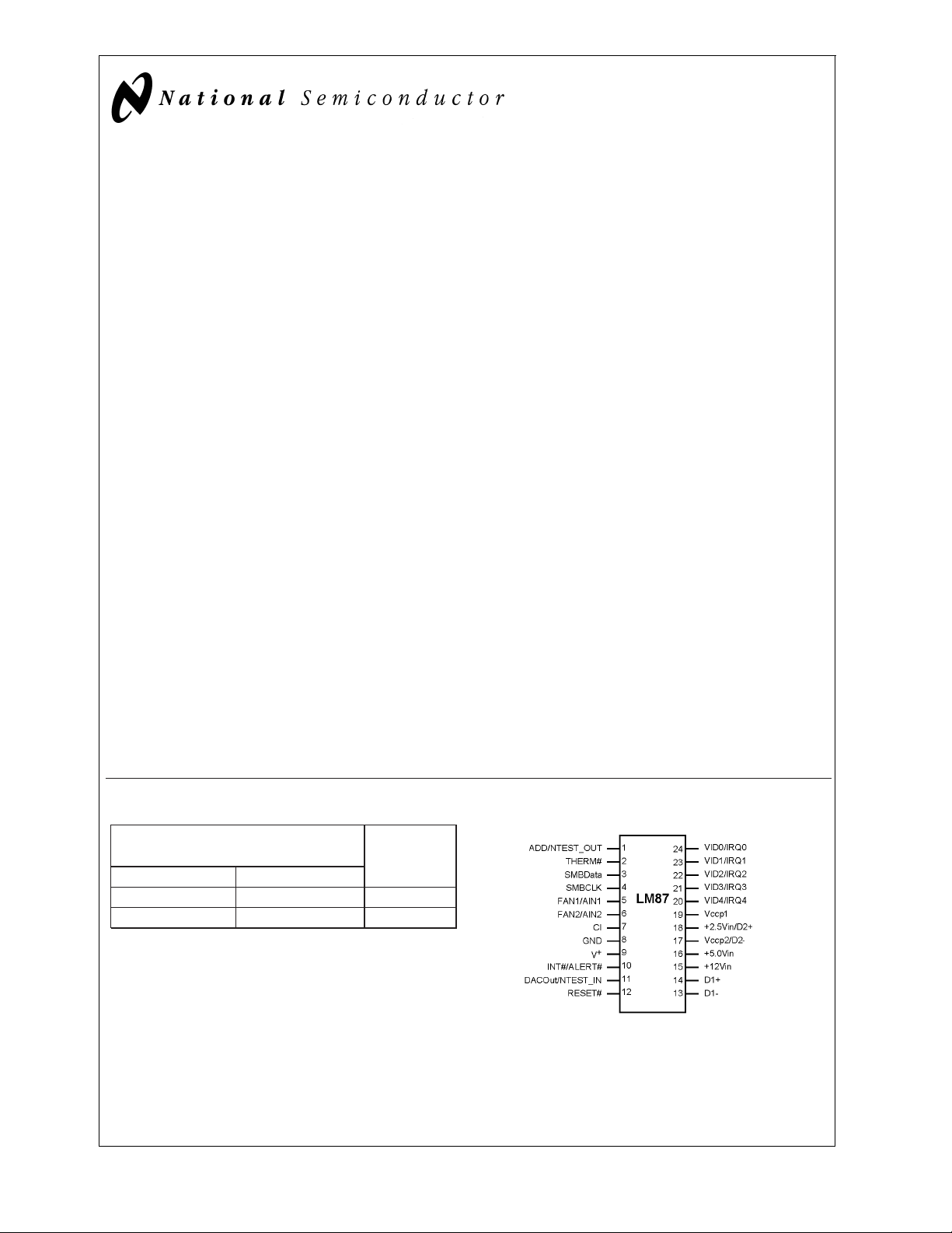
Connection Diagram
DS100995-3
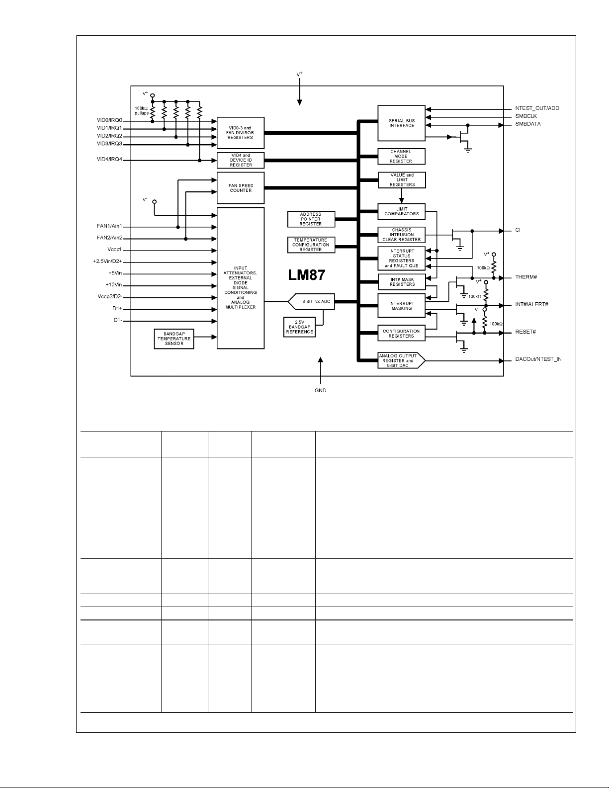
Block Diagram
LM87
DS100995-1
Pin Description
Pin
Name(s)
ADD/NTEST_OUT 1 1 Digital I/0 This pin normally functions as a three-state input that controls the
#
THERM
SMBData 3 1 Digital I/O Serial Bus bidirectional Data. Open-drain output.
SMBCLK 4 1 Digital Input Serial Bus Clock.
FAN1/AIN1-
FAN2/AIN2
CI 7 1 Digital I/O An active high input from an external circuit which latches a
Pin
Number
2 1 Digital I/O This pin functions as an open-drain interrupt output for
5-6 2 Analog/Digital
Number
of Pins
Type Description
two LSBs of the Serial Bus Address. When this pin is tied to V
the two LSBs are 01. When tied to Ground, the two LSBs are 10.
If this pin is not connected, the two LSBs are 00. This pin also
functions as an output during NAND Tree tests (board-level
connectivity testing). To ensure proper NAND tree function, this
pin should not be tied directly to V
5kΩresistor should be used to allow the test output function to
SECTION 11
Inputs
work. Refer to
temperature interrupts only, or as an interrupt input for fan control.
It has an on-chip 100 kΩ pullup resistor.
Programmable as analog inputs (0 to 2.5V) or digital Schmitt
Trigger fan tachometer inputs.
Chassis Intrusion event. This line can go high without any
clamping action regardless of the powered state of the LM87.
There is also an internal open-drain output on this line, controlled
by Bit 7 of the CI Clear Register (46h), to provide a minimum 20
ms reset pulse.
or Ground. Instead, a series
CC
on NAND Tree testing.
CC
www.national.com 2

Pin Description (Continued)
LM87
Pin
Name(s)
GND 8 1 GROUND The system ground pin. Internally connected to all circuitry. The
+
(+2.8 V to
V
+3.8 V)
#
INT
DACOut/NTEST_IN 11 1 Analog
RESET# 12 1 Digital I/O Master Reset, 5 mA driver (open-drain), active low output with a
D1− 13 1 Analog Input Analog input for monitoring the cathode of the first external
D1+ 14 1 Analog Input Analog input for monitoring the anode of the first external
+12Vin 15 1 Analog Input Analog input for monitoring +12 V.
+5Vin 16 1 Analog Input Analog input for monitoring +5 V.
Vccp2/D2− 17 1 Analog Input Digitally programmable analog input for monitoring Vccp2 (0 to 3.6
+2.5Vin/D2+ 18 1 Analog Input Digitally programmable analog input for monitoring +2.5 V or the
Vccp1 19 1 Analog Input Analog input (0 to 3.6 V input range) for monitoring Vccp1, the
VID4/IRQ4VID0/IRQ0
TOTAL PINS 24
/ALERT
#
Pin
Number
9 1 POWER +3.3 V V+power. Bypass with the parallel combination of 10 µF
10 1 Digital Output Interrupt active low open-drain output. This output is enabled when
20-24 5 Digital Inputs Digitally programmable dual function digital inputs. Can be
Number
of Pins
Type Description
ground reference for all analog inputs and the DAC output. This
pin needs to be connected to a low noise analog ground plane for
optimum performance of the DAC output.
(electrolytic or tantalum) and 0.1 µF (ceramic) bypass capacitors.
Bit 1 in the Configuration Register is set to 1. The default state is
disabled. It has an on-chip 100 kΩ pullup resistor. Alternately used
as an active low output to signal SMBus Alert Response Protocol.
0 V to +2.5 V amplitude 8-bit DAC output. When forced high on
Output/Digital
Input
power up by an external voltage the NAND Tree Test mode is
enabled which provides board-level connectivity testing.
45 ms minimum pulse width. Available when enabled via Bit 4 in
the Configuration register. It also acts as an active low power on
RESET input. It has an on-chip 100 kΩ pullup resistor.
temperature sensing diode.
temperature sensing diode.
V input range) or the cathode of the second external temperature
sensing diode.
anode of the second external temperature sensing diode.
core voltage of processore 1.
programmed to monitor the VID pins of the Pentium/PRO and
Pentium II processors, that indicate the operating voltage of the
processor, or as interrupt inputs. The values are read in the
VID/Fan Divisor Register and the VID4 Register. These inputs
have on-chip 100 kΩ pullup resistors.
#
Indicates Active Low (“Not”)
www.national.com3
Absolute Maximum Ratings (Notes 1, 2)
LM87
If Military/Aerospace specified devices are required,
please contact the National Semiconductor Sales Office/
Distributors for availability and specifications.
Positive Supply Voltage (V
+
) +6.0 V
Soldering Information
MTC Package (Note 7) :
Vapor Phase (60 seconds) 215 ˚C
Infrared (15 seconds) 235 ˚C
Storage Temperature −65 ˚C to +150 ˚C
Voltage on Any Input or Output Pin:
+12Vin −0.3 V to +18 V
ADD/NTESTOUT,
DACOut/NTEST_IN, AIN1, AIN2
−0.3 V to
+
+ 0.3 V)
(V
All other pins −0.3 V to +6 V
Input Current at any Pin (Note 4)
Package Input Current (Note 4)
±
Maximum Junction Temperature
max) 150 ˚C
(T
J
ESD Susceptibility (Note 6)
Human Body Model 2000 V
±
5mA
20 mA
Operating Ratings(Notes 1, 2)
Operating Temperature Range T
LM87 −55 ˚C ≤ TA≤ +125 ˚C
Specified Temperature Range T
LM87 −40 ˚C ≤ TA≤ +125 ˚C
Junction to Ambient Thermal Resistance (θ
NS Package Number: MTC24B 95 ˚C/W
+
Supply Voltage (V
Voltage Range:
V
IN
) +2.8 V to +3.8 V
+12Vin −0.05 V to +15 V
MIN
MIN
(Note 5))
JA
+5Vin −0.05 V to +6.8 V
+3.3Vin −0.05 V to +4.6 V
+2.5Vin −0.05 V to +3.6 V
VID0 - VID4, Vccp −0.05 V to +6.0 V
All other inputs −0.05 V to (V
DC Electrical Characteristics
The following specifications apply for +2.8 VDC≤ V+≤ +3.8 VDC, Analog voltage inputs RS= 510 Ω, unless otherwise specified. Boldface limits apply for TA=TJ=T
Symbol Parameter Conditions Typical Limits Units
POWER SUPPLY CHARACTERISTICS
+
I
Supply Current Normal Mode, Interface
TEMPERATURE-TO-DIGITAL CONVERTER CHARACTERISTICS
Temperature Error using Internal Diode
Temperature Error using Remote Pentium
Diode Sensor (Note 11) and (Note 12)
Temperature Error using Remote 2N3904
Sensor (Note 11) and (Note 12)
Resolution 8 bits 1.0 ˚C (min)
LM87 ANALOG-TO-DIGITAL CONVERTER CHARACTERISTICS
Resolution 8 bits
TUE Total Unadjusted Error (Note 13)
DNL Differential Non-Linearity
t
Total Monitoring Cycle Time (Note 14) 0.28 sec
C
ADC INPUT CHARACTERISTICS
Input Resistance (All analog inputs except
AIN1 and AIN2)
AIN1 and AIN2 DC Input Current 12 µA
MIN
to T
; all other limits TA=TJ= 25 ˚C.(Note 8)
MAX
(Note 9) (Note 10) (Limits)
0.7 2.0 mA (max)
Inactive
Shutdown Mode 0.5 mA
±
3˚C
0˚C≤T
≤+125 ˚C, Vcc
A
±
3 ˚C (max)
= 3.3 Vdc
−40 ˚C ≤ T
≤ +125 ˚C,
A
±
4 ˚C (max)
Vcc = 3.3 Vdc
±
2 % (max)
±
1 LSB (max)
130 90 kΩ (min)
≤ TA≤ T
≤ TA≤ T
+
+ 0.05 V)
MAX
MAX
www.national.com 4
DC Electrical Characteristics (Continued)
The following specifications apply for +2.8 VDC≤ V+≤ +3.8 VDC, Analog voltage inputs RS= 510 Ω, unless otherwise specified. Boldface limits apply for TA=TJ=T
Symbol Parameter Conditions Typical Limits Units
DAC CHARACTERISTICS
Resolution 8 Bits
DAC Error 0 ˚C ≤ T
R
C
Output Load Resistance VO= 2.5 V 1250 Ω (min)
L
Output Load Capacitance 20 pF (max)
L
FAN RPM-TO-DIGITAL CONVERTER
Fan RPM Error +25 ˚C ≤ T
Full-scale Count 255 (max)
FAN1 and FAN2 Nominal Input
RPM (See
Section 6.0
)
MIN
to T
; all other limits TA=TJ= 25 ˚C.(Note 8)
MAX
(Note 9) (Note 10) (Limits)
≤ +75 ˚C, V+=
A
3.3 V, Code = 255
+
V
= 3.3 V, 3/4 Scale +8 %
+
V
= 3.3 V, Code =
7(Note 15)
≤ +75 ˚C
A
−10 ˚C ≤ T
−40 ˚C ≤ T
≤ +100 ˚C
A
≤ +125 ˚C
A
Divisor = 1, Fan Count =
153 (Note 16)
Divisor = 2, Fan Count =
153 (Note 16)
Divisor = 3, Fan Count =
153 (Note 16)
Divisor = 4, Fan Count =
153 (Note 16)
±
3.3 % (max)
+4/−2.7 % (max)
±
10 % (max)
±
15 % (max)
±
20 % (max)
8800 RPM
4400 RPM
2200 RPM
1100 RPM
LM87
www.national.com5
DC Electrical Characteristics (Continued)
LM87
The following specifications apply for +2.8 VDC≤ V+≤ +3.8 VDC, Analog voltage inputs RS= 510 Ω, unless otherwise specified. Boldface limits apply for TA=TJ=T
MIN
to T
; all other limits TA=TJ= 25 ˚C.(Note 8)
MAX
Symbol Parameter Conditions Typical Limits Units
(Note 9) (Note 10) (Limits)
DIGITAL OUTPUTS (NTEST_OUT)
V
V
OUT(1)
OUT(0)
Logical “1” Output Voltage I
Logical “0” Output Voltage I
OPEN- DRAIN DIGITAL OUTPUTS (SMBData, RESET
V
V
OUT(0)
OUT(0)
I
Logical “0” Output Voltage (SMBData) I
Logical “0” Output Voltage (Others) I
High Level Output Current V
OH
#
RESET
and Chassis Intrusion 45 20 ms (min)
=±3.0 mA at
OUT
+
= +2.8 V
V
=±3.0 mA at
OUT
+
= +3.8 V
V
#
, CI, INT#, THERM#)
= −755 µA 0.4 V (min)
OUT
=−3mA 0.4 V (min)
OUT
OUT
=V
+
5 12 µA (max)
2.4 V (min)
0.4 V (max)
Pulse Width
DIGITAL INPUTS: VID0–VID4, NTEST_IN, ADD/NTEST_OUT, Chassis Intrusion (CI)
V
IN(1)
V
IN(0)
Logical “1” Input Voltage 2.0 V (min)
Logical “0” Input Voltage 0.8 V (max)
SMBus DIGITAL INPUTS (SMBCLK, SMBData)
V
V
V
IN(1)
IN(0)
HYST
Logical “1” Input Voltage 2.1 V (min)
Logical “0” Input Voltage 0.8 V (max)
Input Hysteresis Voltage 243 mV
Tach Pulse Logic Inputs (FAN1, FAN2)
V
IN(1)
V
IN(0)
Logical “1” Input Voltage 0.7xV
Logical “0” Input Voltage 0.3xV
+
+
ALL DIGITAL INPUTS
I
I
IN(1)
IN(0)
C
Logical “1” Input Current VIN=V
Logical “0” Input Current VIN=0V
Digital Input Capacitance 20 pF
IN
+
DC
−12 µA (min)
12 µA (max)
V (min)
V (max)
www.national.com 6
LM87
AC Electrical Characteristics The following specifications apply for +2.8 V
CLK and SMBData, unless otherwise specified. Boldface limits apply for T
T
= 25˚C. (Note 17)
J
A=TJ=TMIN
≤V+≤ +3.8 VDCon SMB-
DC
to T
; all other limits TA=
MAX
Symbol Parameter Conditions Typical Limits Units
(Note 9) (Note 10) (Limits)
SERIAL BUS TIMING CHARACTERISTICS
t
1
t
rise
t
fall
t
2
t
3
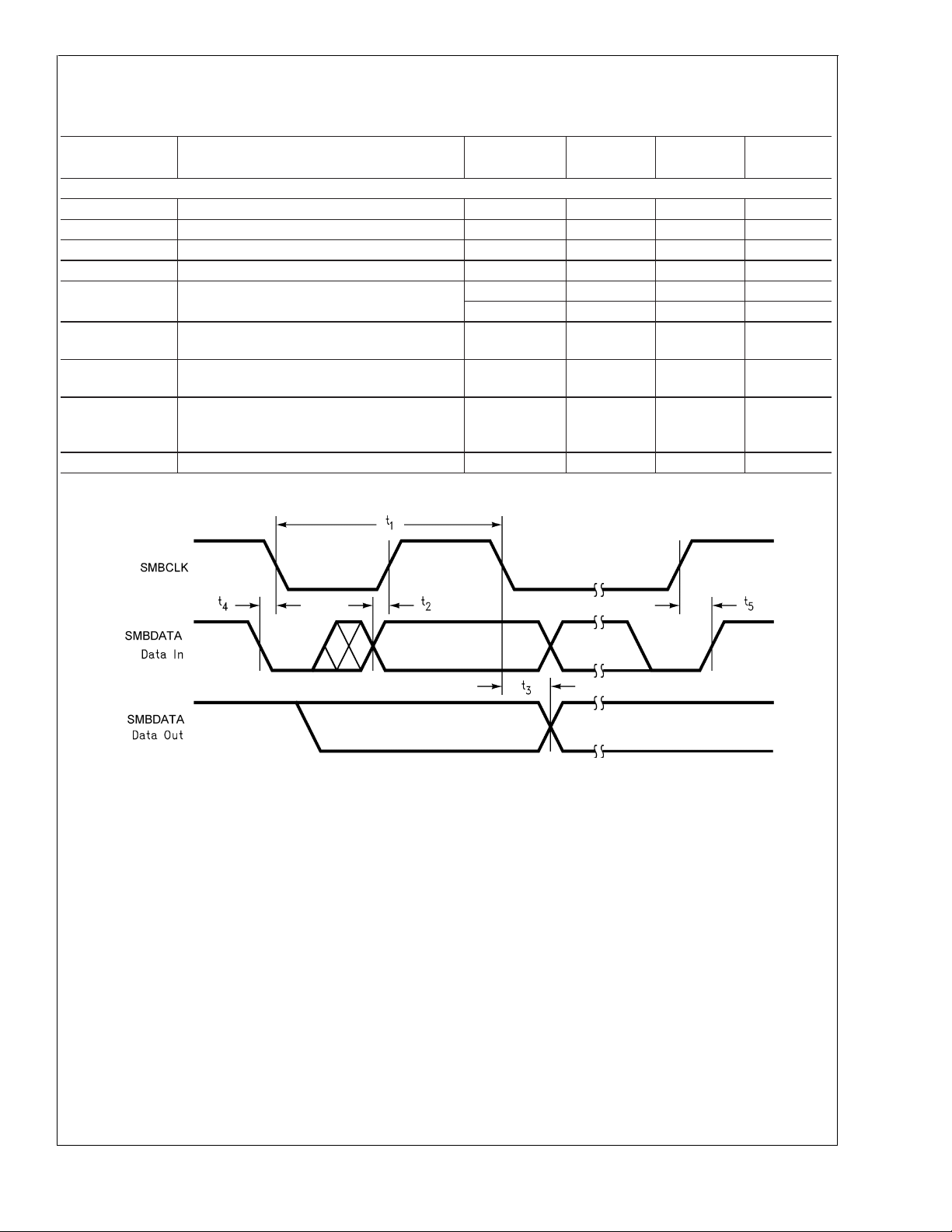
SMBCLK (Clock) Period 2.5 µs (min)
SMBCLK and SMBData Rise Time 1 µs (max)
SMBCLK and SMBData Fall Time 300 ns (max)
Data In Setup Time to SMBCLK High 100 ns (min)
Data Out Stable After SMBCLK Low 100 ns (min)
300 ns (max)
t
4
SMBData Low Setup Time to SMBCLK Low
100 ns (min)
(start)
t
5
SMBData High Hold Time After SMBCLK
100 ns (min)
High (stop)
t
TIMEOUT
C
L
SMBData or SMBCLK low time required to
reset the Serial Bus Interface to the Idle
State
31
25
35
Capacitive Load on SMBCLK and SMBData 80 pF (max)
ms
ms (min)
ms (max)
FIGURE 1. Serial Bus Timing Diagram
DS100995-4
www.national.com7
Electrical Characteristics (Continued)
LM87
Note 1: Absolute Maximum Ratings indicate limits beyond which damage to the device may occur. Operating Ratings indicate conditions for which the device is
functional, but do not guarantee specific performance limits. For guaranteed specifications and test conditions, see the Electrical Characteristics. The guaranteed
specifications apply only for the test conditions listed. Some performance characteristics may degrade when the device is not operated under the listed test conditions.
Note 2: All voltages are measured with respect to GND, unless otherwise specified.
Note 3: The Absolute maximum input range for :
+2.5Vin -−0.3Vto(1.4xV
+3.3Vin -−0.3Vto(1.8xV
Note 4: When the input voltage (V
maximum package input current rating limits the number of pins that can safely exceed the power supplies with an input current of 5 mA to four.
Note 5: Themaximumpower dissipation must be derated at elevatedtemperaturesand is dictated by T
allowable power dissipation at any temperature is P
Note 6: The human body model is a 100 pF capacitor discharged through a 1.5 kΩ resistor into each pin.
Note 7: See the section titled “Surface Mount” found in any post 1986 National Semiconductor Linear Data Book for other methods of soldering surface mountde-
vices.
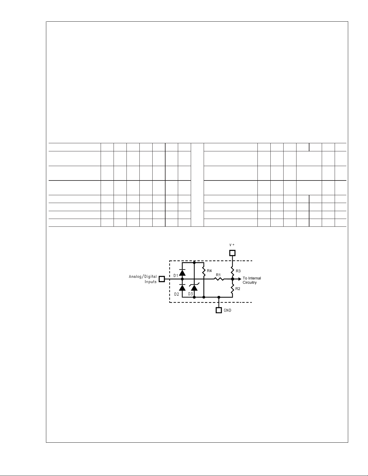
Note 8: Parasitics and or ESD protection circuitryare shown in the figure below for the LM87’s pins.The nominal breakdown voltage of the zener D3 is 6.5 V. Care
should betaken not toforwardbias the parasiticdiode, D1, presentonpins: A0/NTEST_OUT,A1 and DACOut/NTEST_IN. Doingso by morethan 50 mV maycorrupt
a temperature or voltage measurement.
+
+ 0.42 V or 6 V, whichever is smaller
+
+ 0.55 V or 6 V, whichever is smaller.
) at any pin exceeds the power supplies (V
IN
=(TJmax−TA)/θJA.
D
<
IN
GND or V
>
V+), the current at that pin should be limited to 5 mA. The 20 mA
IN
max, θJAand the ambient temperature,TA. The maximum
J
Pin Name D1 D2 D3 R1 R2 R3 R4 Pin Name D1 D2 D3 R1 R2 R3 R4
INT
#
xxx0
∞
100k 1M +12Vin x x R1+R2
≈130k
CI xxx0
∞∞
1M +5Vin x x R1+R2
≈130k
FAN1–FAN2 x x x 0
SMBCLK x x x 0
SMBData x x x 0
#
RESET
xxx0
ADD/NTEST_OUT x x x 0
∞∞
1M +3.3Vin, +2.5Vin,
x x x R1+R2
Vccp1, Vccp2
∞∞
∞∞
∞
∞∞
1M THERM x x x 0
1M VID4–VID0 x x x 0
100k 1M DACOut/NTEST_IN x x x 0
1M
≈130k
∞
∞
∞
∞
100k 1M
∞
100k 1M
∞∞
1M
1M
DS100995-5
An x indicates that the diode exists.
FIGURE 2. ESD Protection Input Structure
Note 9: Typicals are at TJ=TA= 25 ˚C and represent most likely parametric norm.
Note 10: Limits are guaranteed to National’s AOQL (Average Outgoing Quality Level).
Note 11: The Temperature Error specification does not include an additional error of
Note 12: The Temperature Error will vary less than
Note 13: TUE (Total Unadjusted Error) includes Offset, Gain and Linearity errors of the ADC.
Note 14: TotalMonitoring Cycle Time includes all diode checks, temperature conversions and analog input voltage conversions. Fan tachometer readings are de-
termined separately and do not affect the completion of the monitoring cycle.
Note 15: This is the lowest DAC code guaranteed to give a non-zero DAC output.
Note 16: The total fan count is based on 2 pulses per revolution of the fan tachometer output.
Note 17: Timing specifications are tested at the specified logic levels, V
www.national.com 8
±
1˚C over the operating Vcc range of 2.8V to 3.8V.
for a falling edge and VIHfor a rising edge.
IL
±
1˚C, caused by the quantization error.
Test Circuit
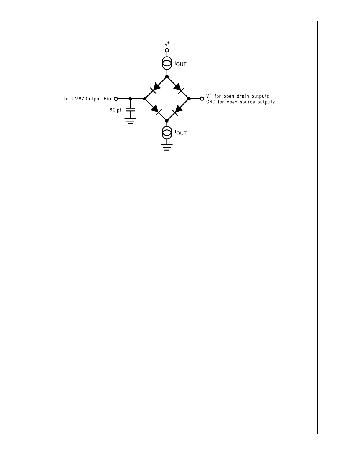
FIGURE 3. Digital Output Load Test Circuitry
Functional Description
1.0 GENERAL DESCRIPTION
The LM87 provides 7 analog inputs, an internal junction type
temperature sensor, two remote junction temperature sensing channels, a Delta-Sigma ADC (Analog-to-Digital Converter), a DAC output, 2 fan speed counters, WATCHDOG
registers, and a variety of inputs and outputs on a single
chip. A two wire SMBus Serial Bus interface is included. The
LM87 performs power supply, temperature, fan control and
fan monitoring for personal computers.
The analog inputs are useful for monitoring several power
supplies present in a typical computer. The LM87 includes
internal resistor dividers that scale external Vccp1, Vccp2,
+2.5V, +5.0 V, +12 V and internal +3.3V power supply voltages to a 3/4 scale nominal ADC output. Two additional inputs, +AIN1 and +AIN2 (2.5V full scale) are input directly
with no resistive dividers. The LM87 ADC continuously converts the scaled inputs to 8-bit digital words. Measurement of
negative voltages (such as -5 V and -12 V power supplies)
can be accommodated with an external resistor divider applied to the +AIN1 or +AIN2 inputs. Internal and external
temperature is converted to 8-bit two’s-complement digital
words witha1˚CLSB.
Fan inputs measure the period of tachometer pulses from
the fans, providing a higher count for lower fan speeds. The
fan inputs are Schmitt-Trigger digital inputs with an acceptable range of0VtoV
mately V
this represents a stopped or very slow fan. Nominal speeds,
based on a count of 153, are programmable from 1100 to
8800 RPM on FAN1 and FAN2. Schmitt-Trigger input circuitry is included to accommodate slow rise and fall times.
An 8 bit DAC with 0 V to 2.5 V output voltage range can be
used for control of fan speed.
The LM87 has several internal registers, as shown in
4
•
•
+
/2. Full scale fan counts are 255 (8-bit counter) and
,
Table 1
and
Section 13.0
Configuration Registers: Provide control and configuration.
Channel Mode Register: Controls the functionality of
the dual purpose input pins, scaling for internal Vcc measurement, and operation of IRQ inputs.
+
and a transition level of approxi-
Figure
. These include:
DS100995-6
Interrupt Status Registers: Two registers to provide
•
status of each WATCHDOG limit or Interrupt event.
Reading the Status Registers clears any active bits.
Interrupt Status Mirror Registers: Two registers to
•
provide status of each WATCHDOG limit or Interrupt
event. Reading the Mirror Registers does not affect the
status bits.
Interrupt Mask Registers: Allows masking of indi-
•
vidual Interrupt sources, as well as separate masking for
each of the two hardware Interrupt outputs.
CI Clear Register: Allows transmitting a 20 ms low
•
pulse on the chassis intrusion pin (CI).
VID/Fan Divisor Register: This register contains the
•
state of the VID0-VID3 input lines and the divisor bits for
FAN1 and FAN2 inputs.
VID4 Register: Contains the state of the VID4 input.
•
Extended Mode Register: Enable and control the
•
Alert Response operation.
Hardware High Limit Registers: Registers at 13h,
•
14h, 17h and 18h where Internal and External ’Hardware’
WATCHDOG temperature high limits are stored. These
limits have Power On Default settings but can be adjusted by the user. The values stored at 13h and 14h can
be locked down by setting bits 1 and 2 of Configuration
Register 2.
LM87
www.national.com9
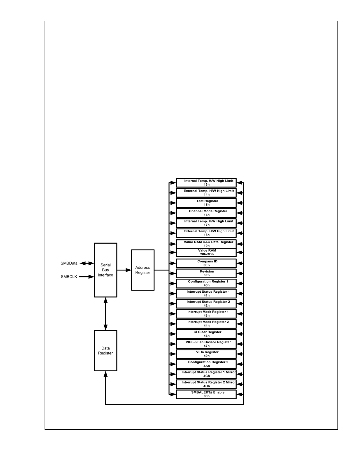
Functional Description (Continued)
LM87
Value and Limit RAM: The DAC digital output, moni-
•
toring results (temperature, voltages, fan counts),
WATCHDOG limits, and Company/Stepping IDs are all
contained in the Value RAM. The Value RAM consists of
a total of 33 bytes, addresses 19h - 3Fh, containing:
— byte 1 at address 19h contains the DAC Data Regis-
ter
— locations 1Ah and 1Bh contain the WATCHDOG low
limits for AIN1 and AIN2
— locations 1Ch - 1Fh are unassigned and do not have
associated registers
— the next 10 bytes at addresses 20h -29h contain all of
the results
— location 2Ah is unassigned and does not have an as-
sociated register
— the next 18 bytes at addresses 2Bh-3Ch are the re-
maining WATCHDOG limits
— the last 2 bytes at addresses 3Eh and 3Fh contain the
Company ID and Stepping ID numbers, respectively
2.0 INTERFACE
When the LM87 is started, it cycles through each measurement in sequence, and it continuously loops through the sequence approximately once every 0.4 s. Each measured
value is compared to values stored in WATCHDOG,orHardware High Limit registers. When the measured value violates
the programmed limit the LM87 will set a corresponding Interrupt in the Interrupt Status Registers. The hardware Interrupt line INT
of each Interrupt source. In addition, the Configuration Register has a control bit to enable or disable the hardware Interrupt. Another hardware Interrupt line available, THERM
used to signal temperature specific events. Having a dedicated interrupt for these conditions allows specific actions to
be taken for thermal events. This output is enabled by setting
bit 2 of Configuration Register 1.
The Chassis Intrusion input is designed to accept an active
high signal from an external circuit that activates and latches
when the case is removed from the computer.
#
is fully programmable with separate masking
#
is
FIGURE 4. LM87 Register Structure
www.national.com 10
DS100995-7
 Loading...