

NSC LM8333FLQ8X, LM8333 Datasheet
August 2007
LM8333
Mobile I/O Companion Supporting Key-Scan, I/O
Expansion, PWM, and ACCESS.bus Host Interface
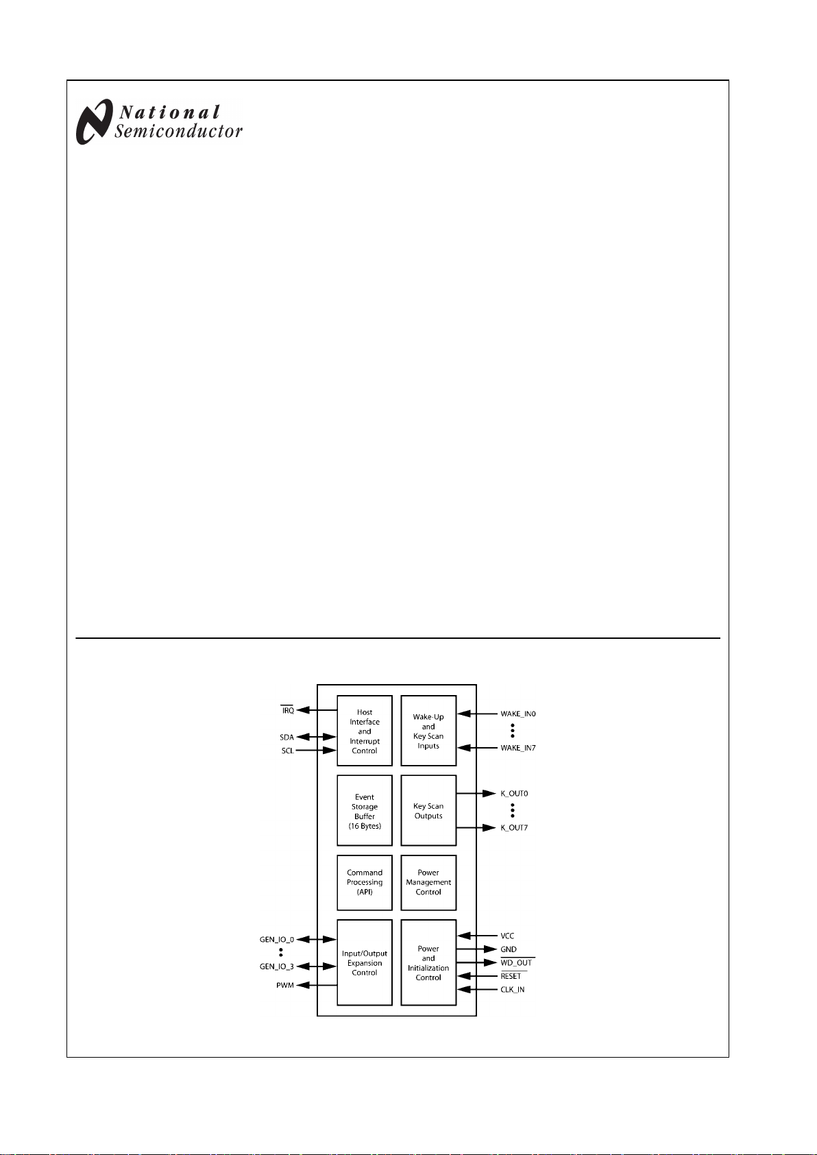
1.0 General Description
The LM8333 Mobile I/O Companion offloads the burden of
keyboard scanning from the host, while providing extremely
low power consumption in both operational and standby
modes. It supports keypad matrices up to 8 × 8 in size (plus
another 8 special-function keys), for portable applications
such as cellphones, PDAs, games, and other handheld applications.
Key press and release events are encoded into a byte format
and loaded into a FIFO buffer for retrieval by the host processor. An interrupt output (IRQ) is used to signal events such
as keypad activity, a state change on either of two interruptcapable general-purpose I/O pins, or an error condition. Interrupt and error codes are available to the host by reading
dedicated registers.
Four general-purpose I/O pins are available, two of which
have interrupt capability. A pulse-width modulated output
based on a host-programmable internal timer is also available, which can be used as a general-purpose output if the
PWM function is not required.
To minimize power, the LM8333 automatically enters a lowpower standby mode when there is no keypad, I/O, or host
activity.
The device is packaged in a 32–pin Leadless Leadframe
package (LLP) and a 49-pin MICRO-ARRAY . Both are chipscale packages.
2.0 Features
■
8 × 8 standard keys
■
8 special function keys (SF keys) providing a total of 72
keys for the maximum keyboard matrix
■
ACCESS.bus (I2C-compatible) communication interface
to the host
■
Four general purpose host programmable I/O pins with
two optional (slow) external Interrupts
■
16 byte FIFO buffer to store key pressed and key released
events
■
Error control with error reports on (FIFO overrun, Keypad
overrun, invalid command)
■
Host programmable PWM
■
Host programmable active time and debounce time
3.0 Applications
■
Mobile phones
■
Personal Digital Assistants (PDAs)
■
Smart handheld devices
■
Personal media players
4.0 Block Diagram
20210601
I2C® is a registered trademark of Phillips Corporation.
© 2007 National Semiconductor Corporation 202106 www.national.com
LM8333 Mobile I/O Companion Supporting Key-Scan, I/O Expansion, PWM, and ACCESS.bus
Host Interface
5.0 Ordering Information
NSID Spec. No. of Pins Package Type Temperature Package Method
LM8333FLQ8X NOPB 32 LLP −40 to + 85°C 2500 pcs Tape & Reel
LM8333FLQ8Y NOPB 32 LLP −40 to + 85°C 250 pcs Tape & Reel
LM8333GGR8 NOPB 49 Micro-array −40 to + 85°C 1000 pcs Tape & Reel
NOPB = No PB (No Lead)
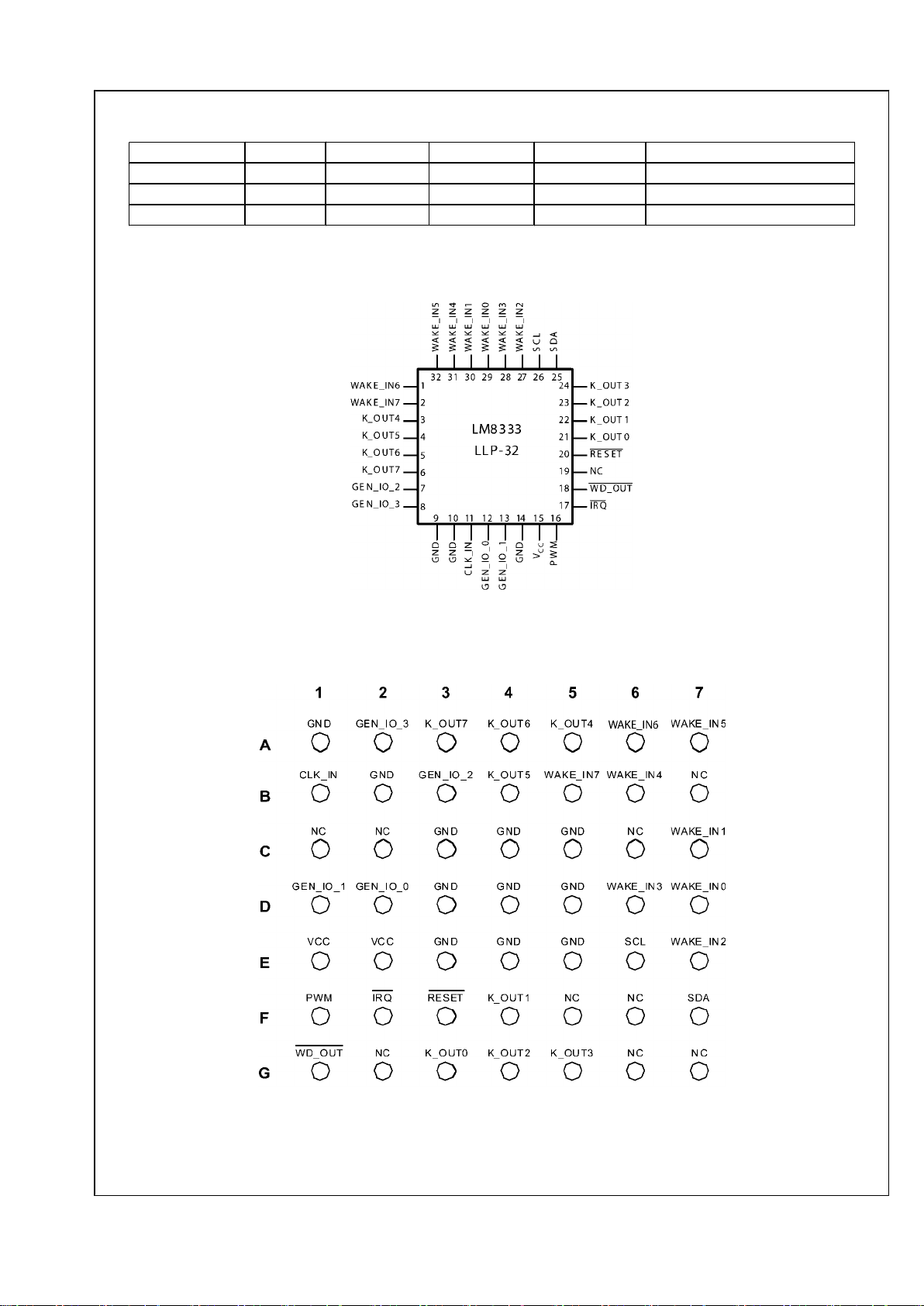
6.0 Pin Assignments
20210649
Top View
Leadless Leadframe Package
See NS Package Number LQA32A
20210602
Top View
MICRO-ARRAY Package
See NS Package Number GRA49A
www.national.com 2
LM8333

Table of Contents
1.0 General Description ......................................................................................................................... 1
2.0 Features ........................................................................................................................................ 1
3.0 Applications .................................................................................................................................... 1
4.0 Block Diagram ................................................................................................................................ 1
5.0 Ordering Information ........................................................................................................................ 2
6.0 Pin Assignments ............................................................................................................................. 2
7.0 Signal Descriptions .......................................................................................................................... 4
8.0 Typical Application ........................................................................................................................... 5
8.1 FEATURES .................................................................................................................................. 5
8.2 I/O EXPANSION OPTIONS ............................................................................................................ 5
8.3 WATCHDOG TIMER ..................................................................................................................... 5
8.4 HALT MODE ................................................................................................................................ 5
8.4.1 ACCESS.bus Activity ................................................................................................................ 5
8.5 KEYPAD SCANNING ..................................................................................................................... 6
8.6 COMMUNICATION INTERFACE ..................................................................................................... 6
8.6.1 Interrupts Between the Host and LM8333 ..................................................................................... 6
8.6.2 Interrupt Sources ...................................................................................................................... 6
9.0 Device Operation ............................................................................................................................ 6
9.1 EVENT CODE ASSIGNMENT ......................................................................................................... 6
9.2 I/O EXPANSION ........................................................................................................................... 7
9.2.1 PWM Output with Programmable Duty Cycle ................................................................................ 7
9.2.2 General-Purpose I/O (GPIO) ...................................................................................................... 8
9.2.3 External Interrupts .................................................................................................................... 8
9.3 HOST COMMAND EXECUTION ..................................................................................................... 9
9.3.1 Command Structure .................................................................................................................. 9
9.4 HOST WRITE COMMANDS ......................................................................................................... 10
9.5 HOST READ COMMANDS ........................................................................................................... 10
9.6 WAKE-UP FROM HALT MODE ..................................................................................................... 11
10.0 Interrupts .................................................................................................................................... 11
10.1 INTERRUPT CODE ................................................................................................................... 11
10.2 ERROR CODE .......................................................................................................................... 11
10.3 STATUS CODES ....................................................................................................................... 12
10.4 INTERRUPT PROCESSING ....................................................................................................... 12
10.5 COMMAND EXECUTION SUMMARY .......................................................................................... 13
11.0 Absolute Maximum Ratings ........................................................................................................... 14
12.0 DC Electrical Characteristics ......................................................................................................... 14
13.0 AC Electrical Characteristics ......................................................................................................... 15
14.0 Physical Dimensions .................................................................................................................... 17
3 www.national.com
LM8333

7.0 Signal Descriptions
Name 32 Pins 49 Pins I/O Description
WAKE_IN0 29 D7 Input Wake-up input/Keyboard scanning input 0
WAKE_IN1 30 C7 Input Wake-up input/Keyboard scanning input 1
WAKE_IN2 27 E7 Input Wake-up input/Keyboard scanning input 2
WAKE_IN3 28 D6 Input Wake-up input/Keyboard scanning input 3
WAKE_IN4 31 B6 Input Wake-up input/Keyboard scanning input 4
WAKE_IN5 32 A7 Input Wake-up input/Keyboard scanning input 5
WAKE_IN6 1 A6 Input Wake-up input/Keyboard scanning input 6
WAKE_IN7 2 B5 Input Wake-up input/Keyboard scanning input 7
K_OUT0 21 G3 Output Keyboard scanning output 0
K_OUT1 22 F4 Output Keyboard scanning output 1
K_OUT2 23 G4 Output Keyboard scanning output 2
K_OUT3 24 G5 Output Keyboard scanning output 3
K_OUT4 3 A5 Output Keyboard scanning output 4
K_OUT5 4 B4 Output Keyboard scanning output 5
K_OUT6 5 A4 Output Keyboard scanning output 6
K_OUT7 6 A3 Output Keyboard scanning output 7
GEN_IO_0 12 D2 I/O General-purpose I/O 0
GEN_IO_1 13 D1 I/O General-purpose I/O 1
GEN_IO_2 7 B3 I/O General-purpose I/O 2
GEN_IO_3 8 A2 I/O General-purpose I/O 3
SDA 25 F7 I/O ACCESS.bus data signal
SCL 26 E6 Input ACCESS.bus clock signal
IRQ 17 F2 Output Interrupt request output
PWM 16 F1 Output Pulse-width modulated output
WD_OUT 18 G1 Output Watchdog timer output (connect to RESET input)
RESET 20 F3 Input Reset input
CLK_IN 11 B1 Input Clock input (connect to ground through a 68k ohm resistor)
VCC 15 E1, E2 n.a. Vcc
GND 9, 10, 14 A1, B2, C3,
C4, C5, D3,
D4, D5, E3,
E4, E5
n.a. Ground
NC 19 B7, C1, C2,
C6, F5, F6,
G2, G6, G7
n.a. No connect
www.national.com 4
LM8333
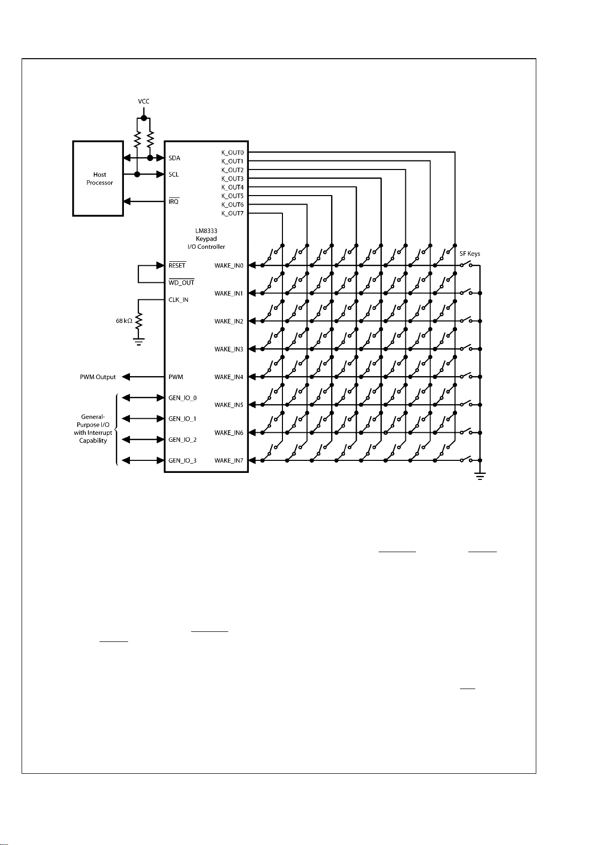
8.0 Typical Application
20210603
FIGURE 1. Typical Keypad Configuration
8.1 FEATURES
The following features are supported:
•
8 x 8 standard keys.
•
8 special function keys (SF keys) with wake-up capability
by forcing a WAKE_INx pin to ground. Pressing a SF key
overrides any other key in the same row.
•
A total of 72 keys can be scanned.
•
ACCESS.bus (I2C-compatible) interface for
communication with the host.
•
The watchdog timer is mandatory, so WD_OUT
must be
connected to RESET.
8.2 I/O EXPANSION OPTIONS
•
One host-programmable PWM output which also may be
used as a general-purpose output.
•
Four host-programmable general-purpose I/O pins,
GEN_IO_0, GEN_IO_1, GEN_IO_2, and GEN_IO_3.
GEN_IO_0 and GEN_IO_1 can also be configured for
“slow” interrupts, in which any transition will trigger a
hardware interrupt event to the host.
8.3 WATCHDOG TIMER
The watchdog timer is always enabled in hardware. To use
the timer, connect the WD_OUT
output to the RESET input.
8.4 HALT MODE
The fully static architecture of the LM8333 allows stopping the
internal RC clock in Halt mode, which reduces power consumption to the minimum level.
Halt mode is entered when no key-press, key-release, or
ACCESS.bus activity is detected for a certain period of time
(by default, 500 milliseconds). The mechanism for entering
Halt mode is always enabled in hardware, but the host can
program the period of inactivity which triggers entry into Halt
mode.
The LM8333 will remain in Active mode as long as a key
event, or any other event, which causes the IRQ output to be
asserted is not resolved.
8.4.1 ACCESS.bus Activity
When the LM8333 is in Halt mode, any activity on the
ACCESS.bus interface will cause the LM8333 to exit from
Halt mode. However, the LM8333 will not be able to acknowl-
5 www.national.com
LM8333

edge the first bus cycle immediately following wake-up from
Halt mode. It will respond with a negative acknowledgement,
and the host should then repeat the cycle.
The LM8333 will be prevented from entering Halt mode if it
shares the bus with peripherals that are continuously active.
For lowest power consumption, the LM8333 should only
share the bus with peripherals that require little or no bus activity after system initialization.
8.5 KEYPAD SCANNING
The LM8333 starts new scanning cycles at fixed time intervals
of about 4 ms. If a change in the state of the keypad is detected, the keypad is rescanned after a debounce delay.
When the state change has been reliably captured, it is encoded and written to the FIFO buffer.
If more than two keys are pressed simultaneously, the pattern
of key closures may be ambiguous, so pressing more than
two keys asserts the Error Flag condition and the IRQ output
(if enabled). The host may attempt to interpret the events
stored in the FIFO or discard them.
The SF keys connect the WAKE_INx pins directly to ground.
There can be up to eight SF-keys. If any of these keys are
pressed, other key presses that use the same WAKE_INx pin
will be ignored.
8.6 COMMUNICATION INTERFACE
The two-wire ACCESS.bus interface is used to communicate
with a host. The ACCESS.bus interface is fully compliant with
the I2Cbus standard. The LM8333 operates as a bus slave at
speeds up to 400 kHz.
An ACCESS.bus transfer starts with a byte that includes a 7bit slave device address. The LM8333 responds to a fixed
device address. This address is 0xA2, when aligned to the
MSB (7-bit address mapped to bits 7:1, rather than bits 6:0).
Bit 0 is a direction bit (0 on write, 1 on read).
Because it is a slave, the LM8333 never initiates an
ACCESS.bus cycle, it only responds to bus cycles initiated by
the host. The LM8333 may signal events to the host by asserting the IRQ interrupt request.
8.6.1 Interrupts Between the Host and LM8333
The IRQ output is used to signal unresolved interrupts, errors,
and key-events to the host.
The host can use an available GEN_IO_0 or GEN_IO_1 pin
to interrupt (or wake-up) the LM8333, if it is not being used for
another function. The host can also wake-up the LM8333 by
sending a Start Condition on the ACCESS.bus interface.
Note:
The LM8333 it will not be able to acknowledge the first byte received
from the host after wake-up. In this case, the host will have to resend
the slave address.
8.6.2 Interrupt Sources
The IRQ
output is asserted on these conditions:
•
Any new key-event.
•
Any error condition, which is indicated by the error code.
•
Any enabled interrupt on either of the GEN_IO_0 or
GEN_IO_1 pins that can be configured as external
interrupt inputs. When enabled, any rising or falling edge
triggers an interrupt.
The IRQ output remains asserted until the interrupt code is
read.
9.0 Device Operation
9.1 EVENT CODE ASSIGNMENT
After power-on reset, the LM8333 starts scanning the keypad.
It stays active for a default time of about 500 ms after the last
key is released, after which it enters a standby mode to minimize power consumption (<2 µA standby current).
Table 1 lists the codes assigned to the matrix positions encoded by the hardware. Key-press events are assigned the
codes listed in Table 1, but with the MSB set. When a key is
released, the MSB of the code is clear.
TABLE 1. Keypad Matrix Code Assignments
K_OUT0 K_OUT1 K_OUT2 K_OUT3 K_OUT4 K_OUT5 K_OUT6 K_OUT7 SF Keys
WAKE_IN0 0x01 0x02 0x03 0x04 0x05 0x06 0x07 0x08 0x09
WAKE_IN1 0x11 0x12 0x13 0x14 0x15 0x16 0x17 0x18 0x19
WAKE_IN2 0x21 0x22 0x23 0x24 0x25 0x26 0x27 0x28 0x29
WAKE_IN3 0x31 0x32 0x33 0x34 0x35 0x36 0x37 0x38 0x39
WAKE_IN4 0x41 0x42 0x43 0x44 0x45 0x46 0x47 0x48 0x49
WAKE_IN5 0x51 0x52 0x53 0x54 0x55 0x56 0x57 0x58 0x59
WAKE_IN6 0x61 0x62 0x63 0x64 0x65 0x66 0x67 0x68 0x69
WAKE_IN7 0x71 0x72 0x73 0x74 0x75 0x76 0x77 0x78 0x79
The codes are loaded into the FIFO buffer in the order in
which they occurred. Table 2 shows an example sequence of
events, and Figure 2 shows the resulting sequence of event
codes loaded into the FIFO buffer.
www.national.com 6
LM8333
 Loading...