

NSC LM831N Datasheet
LM831 Low Voltage Audio Power Amplifier
LM831 Low Voltage Audio Power Amplifier
December 1994
General Description
The LM831 is a dual audio power amplifier optimized for
very low voltage operation. The LM831 has two independent amplifiers, giving stereo or higher power bridge (BTL)
operation from two- or three-cell power supplies.
The LM831 uses a patented compensation technique to reduce high-frequency radiation for optimum performance in
AM radio applications. This compensation also results in
lower distortion and less wide-band noise.
The input is direct-coupled to the LM831, eliminating the
usual coupling capacitor. Voltage gain is adjustable with a
single resistor.
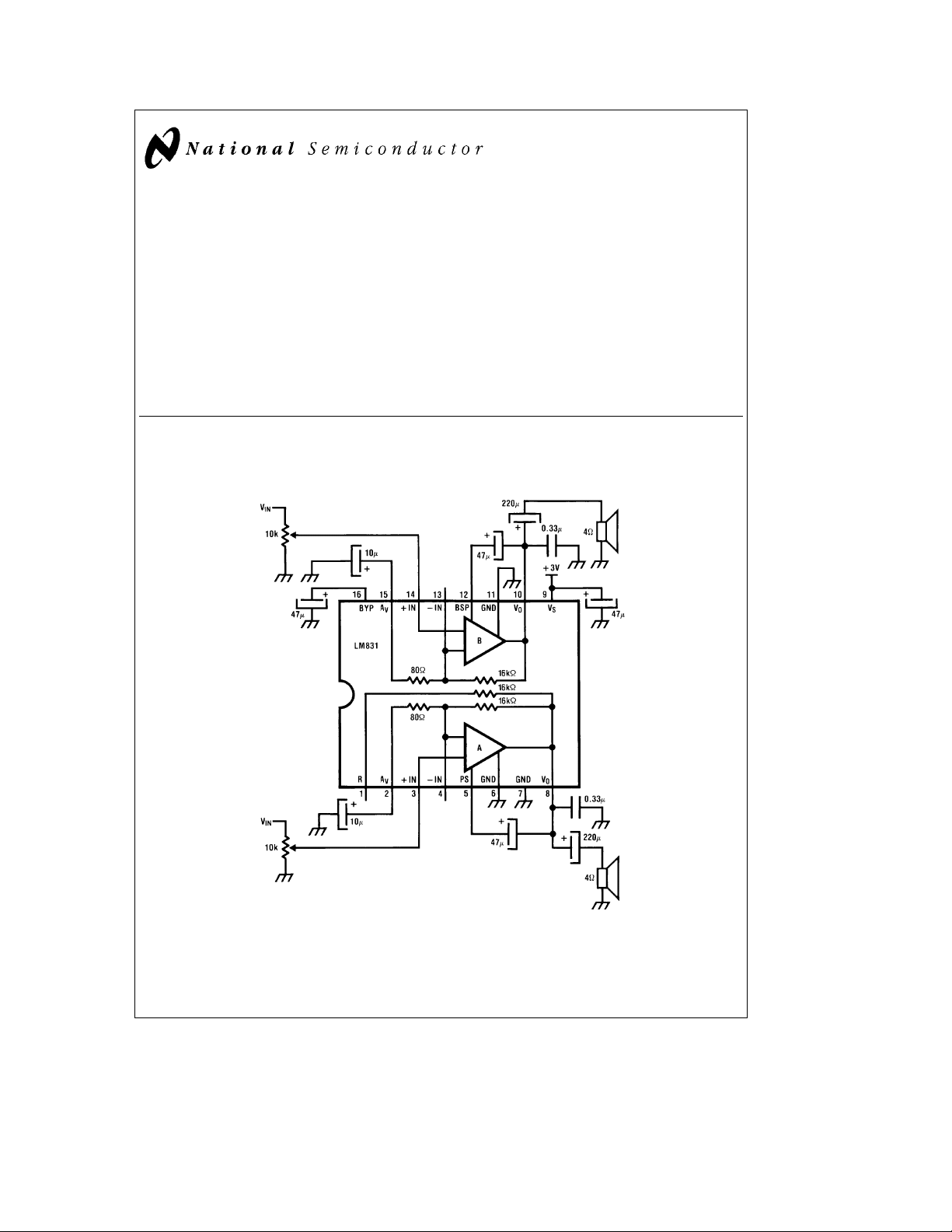
Typical Application
Dual Amplifier with Minimum Parts
Features
Y
Low voltage operation, 1.8V to 6.0V
Y
High power, 440 mW, 8X, BTL, 3V
Y
Low AM radiation
Y
Low noise
Y
Low THD
Applications
Y
Portable tape recorders
Y
Portable radios
Y
Headphone stereo
Y
Portable speakers
TL/H/6754– 1
e
A
46 dB,BWe250 Hz to 35 kHz
V
e
P
220 mW/Ch,R
OUT
C
1995 National Semiconductor Corporation RRD-B30M115/Printed in U. S. A.
TL/H/6754
e
4X
L
Absolute Maximum Ratings
If Military/Aerospace specified devices are required,
please contact the National Semiconductor Sales
Office/Distributors for availability and specifications.
Supply Voltage, V
Input Voltage, V
Power Dissipation (Note 1), P
S
IN
D
Operating Temperature (Note 1), T
1.3W (M Package)
1.4W (N Package)
b
opr
40§Ctoa85§C
7.5V
g
0.4V
b
Storage Temperature, T
Junction Temperature, T
Lead Temp. (Soldering, 10 sec.), T
stg
j
Thermal Resistance
i
(DIP) 27§C/W
JC
i
(DIP) 75§C/W
JA
i
(SO Package) 20§C/W
JC
i
(SO Package) 95§C/W
JA
65§Ctoa150§C
L
a
a
150§C
260§C
Electrical Characteristics
Unless otherwise specified, T
e
25§C, V
A
Symbol Parameter Conditions Typ Tested Limit Unit (Limit)
V
S
I
Q
V
OS
R
IN
A
V
Operating Voltage 3 1.8 V(Min)
Supply Current V
Output DC Offset V
Input Resistance 25 15 k (Min)
Voltage Gain V
PSRR Supply Rejection V
P
OD
P
ODL
P
OB
P
OBL
Power Out V
Power Out Low, V
S
Power Out V
Power Out Low, V
S
Sep Channel Separation Referenced to V
I
B
E
n0
Input Bias Current 1 2 mA (Max)
Output Noise Wide Band (250E35 kHz) 250 500 mV (Max)
THD Distortion V
Note 1: For operation in ambient temperatures above 25§C, the device must be derated based on a 150§C maximum junction temperature and a thermal resistance
C/W junction to ambient for the M package or 90§C/W junction to ambient for the N package.
of 98
§
e
3V, fe1 kHz, test circuit is dual or BTL amplifier with minimum parts.
S
3 6 V(Max)
e
0, Dual Mode 5 10 mA (Max)
IN
e
0, BTL Mode 6 15 mA (Max)
V
IN
e
0, BTL Mode 10 50 mV (Max)
IN
35 k (Max)
e
2.25 mV
IN
Dual Mode 48 dB (Max)
e3Va
S
e
3V, R
S
10% THD, Dual Mode
e
V
1.8V, R
S
10% THD, Dual Mode
e
3V, R
S
10% THD, BTL Mode
e
V
1.8V, R
S
10% THD, BTL Mode
e
3V, P
S
e
f
1 kHz, Dual
,fe1 kHz, 46 44 dB (Min)
rms
4X,
e
4X,
8X,
e
8X,
e
O
50 mW,
@
fe1 kHz 46 30 dB (Min)
rms
220 150 mW (Min)
45 10 mW (Min)
440 300 mW (Min)
90 20 mW (Min)
200 mV
rms
52 40 dB (Min)
0.25 1 % (Max)
200 mV
e
L
L
e
L
L
e
O
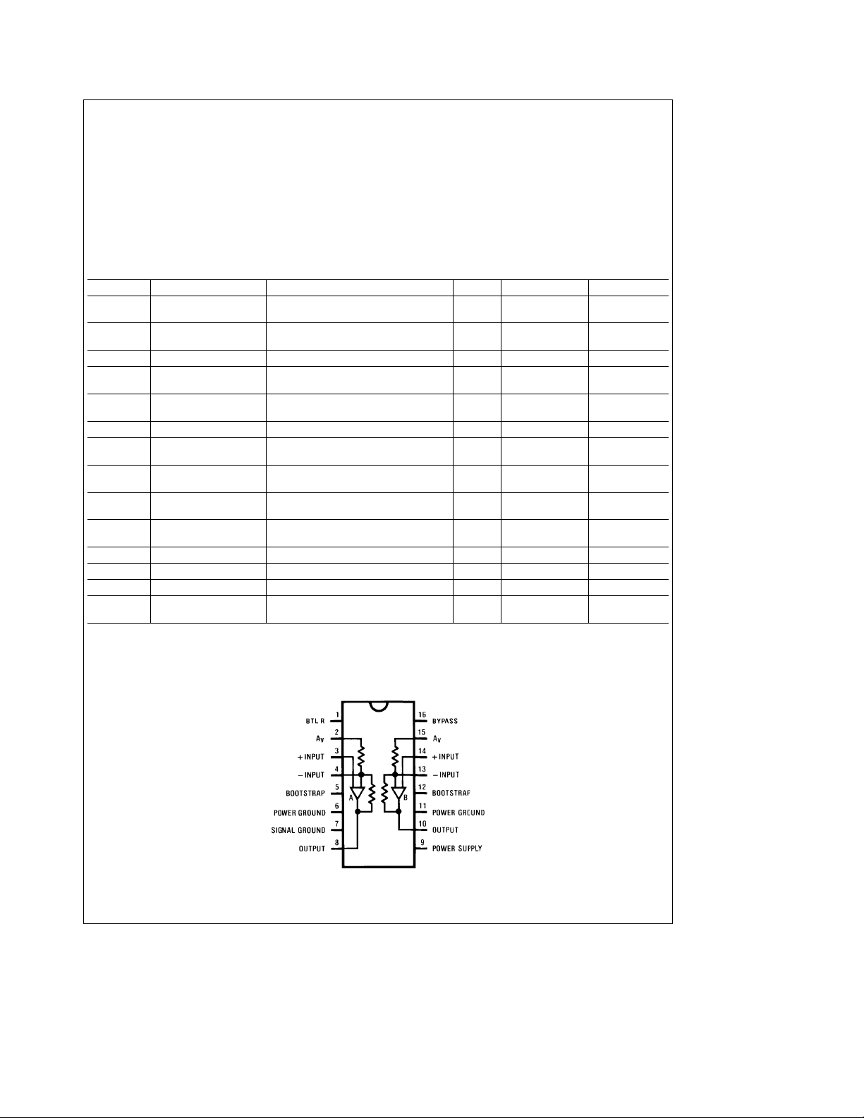
Connection Diagram
Dual-In-Line Package
TL/H/6754– 2
Top View
Order Number LM831M or N
See NS Package Number M16B or N16E
2
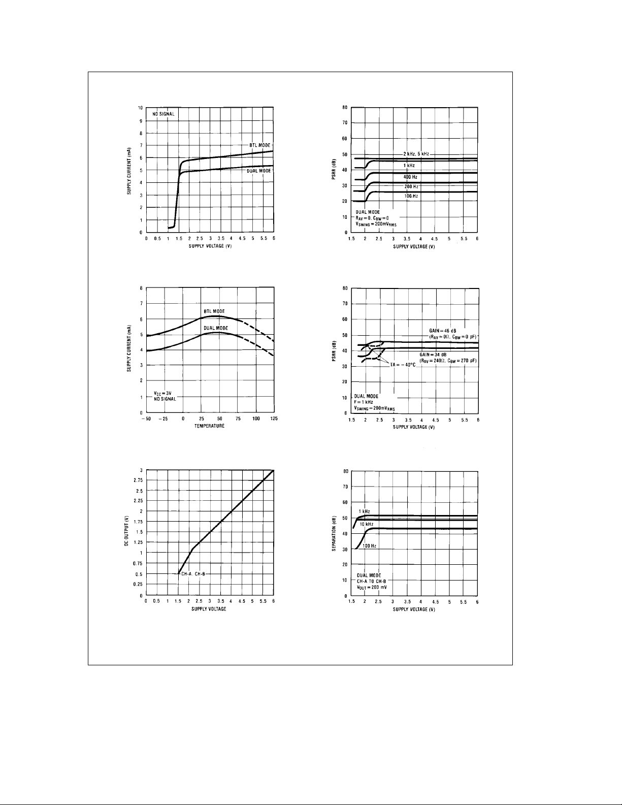
Typical Performance Characteristics
Supply Current vs Supply Voltage PSRR vs Supply Voltage
Supply Current vs Temperature PSRR vs Supply Voltage
DC Output vs Supply Voltage Separation vs Supply Voltage
3
TL/H/6754– 4
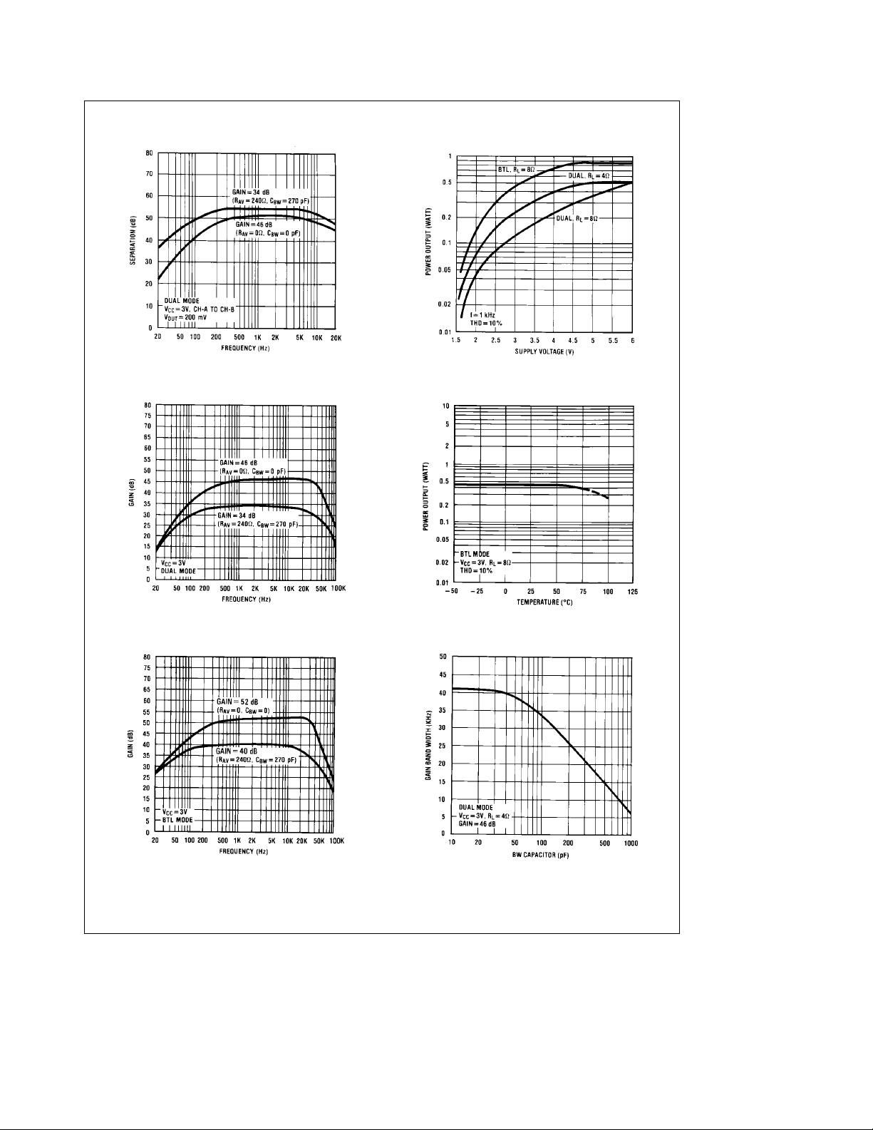
Typical Performance Characteristics (Continued)
Separation vs Frequency Power Output vs Supply Voltage
Gain vs Frequency Power Output vs Temperature
Gain vs Frequency Bandwidth vs BW Capacitance
4
TL/H/6754– 5
Typical Performance Characteristics (Continued)
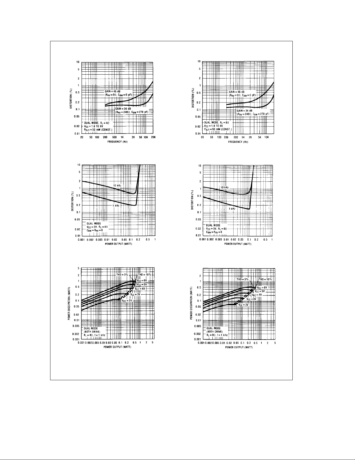
e
Dual Mode, R
Distortion vs Power Output (Note 2) Distortion vs Power Output (Note 2)
4X Distortion vs Frequency Dual Mode, R
L
e
8X Distortion vs Frequency
L
Power Dissipation vs Power Output Power Dissipation vs Power Output
5
TL/H/6754– 6
 Loading...