

NSC LM828M5X, LM828M5 Datasheet
LM828
Switched Capacitor Voltage Converter
LM828 Switched Capacitor Voltage Converter
March 1999
General Description
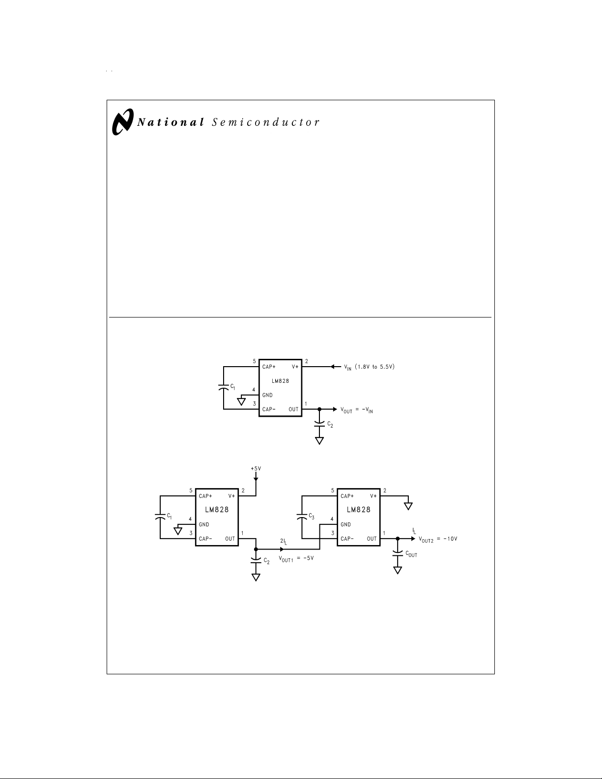
The LM828 CMOS charge-pump voltage converter inverts a
positive voltage in the range of +1.8V to +5.5V to the corresponding negative voltage of −1.8V to −5.5V. The LM828
uses two low cost capacitors to provide up to 25 mA of output current.
The LM828 operates at 12 kHz switching frequency to reduce output resistance and voltageripple.With an operating
current of only 40 µA (operating efficiency greater than 96
with most loads), the LM828 provides ideal performance for
battery powered systems. The device is in a tiny SOT-23-5
package.
Basic Application Circuits
Voltage Inverter
+5V to −10V Converter
Features
n Inverts Input Supply Voltage
n SOT-23-5 Package
n 20Ω Typical Output Impedance
n 97%Typical Conversion Efficiency at 5 mA
Applications
n Cellular Phones
%
n Pagers
n PDAs
n Operational Amplifier Power Supplies
n Interface Power Supplies
n Handheld Instruments
DS100137-1
DS100137-2
© 1999 National Semiconductor Corporation DS100137 www.national.com
Absolute Maximum Ratings (Note 1)
If Military/Aerospace specified devices are required,
please contact the National Semiconductor Sales Office/
Distributors for availability and specifications.
Supply Voltage (V+ to
GND, or GND to OUT)
V+ and OUT Continuous
Output Current
Output Short-Circuit
5.8V
50 mA
1 sec.
T
(Note 3) 150˚C
JMax
θ
(Note 3) 300˚C/W
JA
Operating Junction
−40˚C to 85˚C
Temperature Range
Storage Temperature
−65˚C to +150˚C
Range
Lead Temp. (Soldering, 10
300˚C
seconds)
ESD Rating (Note 7) 2kV
Duration to GND (Note 2)
Continuous Power
Dissipation (T
25˚C)(Note 3)
=
A
240 mW
Electrical Characteristics
Limits in standard typeface are for T
less otherwise specified: V+=5V, C
Symbol Parameter Condition Min Typ Max Units
V+ Supply Voltage R
I
Q
R
OUT
f
OSC
f
SW
P
EFF
V
OEFF
Note 1: Absolute maximum ratings indicate limits beyond which damage to the device may occur. Electrical specifications do not apply when operating the device
beyond its rated operating conditions.
Note 2: OUT may be shorted to GND for one second without damage. However, shorting OUT to V+ may damage the device and should be avoided. Also, for temperatures above 85˚C, OUT must not be shorted to GND or V+, or the device may be damaged.
Note 3: The maximum allowable power dissipation is calculated by using P
ambient temperature, and θ
Note 4: In the test circuit, capacitors C
voltage and efficiency.
Note 5: Specified output resistance includes internal switch resistance and capacitor ESR. See the details in the application information.
Note 6: The output switches operate at one half of the oscillator frequency, f
Note 7: The human body model is a 100 pF capacitor discharged through a 1.5 kΩ resistor into each pin.
Supply Current No Load 40 75 µA
Output Resistance (Note 5) I
Oscillator Frequency (Note 6) Internal 12 24 56 kHz
Switching Frequency (Note 6) Measured at CAP+ 6 12 28 kHz
Power Efficiency I
Voltage Conversion Efficiency No Load 95 99.96
is the junction-to-ambient thermal resistance of the package.
JA
=
25˚C, and limits in boldface type apply over the full operating temperature range. Un-
J
=
=
C
10 µF. (Note 4)
1
2
=
10kΩ 1.8 5.5 V
L
115
=
5mA 20 65 Ω
L
=
5mA 97
L
=
DMax
and C2are 10 µF,0.3ΩmaximumESRcapacitors.Capacitors with higher ESR will increase output resistance, reduce output
1
=
OSC
(T
JMax−TA
2f
SW
.
)/θJA, where T
is the maximum junction temperature, TAis the
JMax
%
%
www.national.com 2
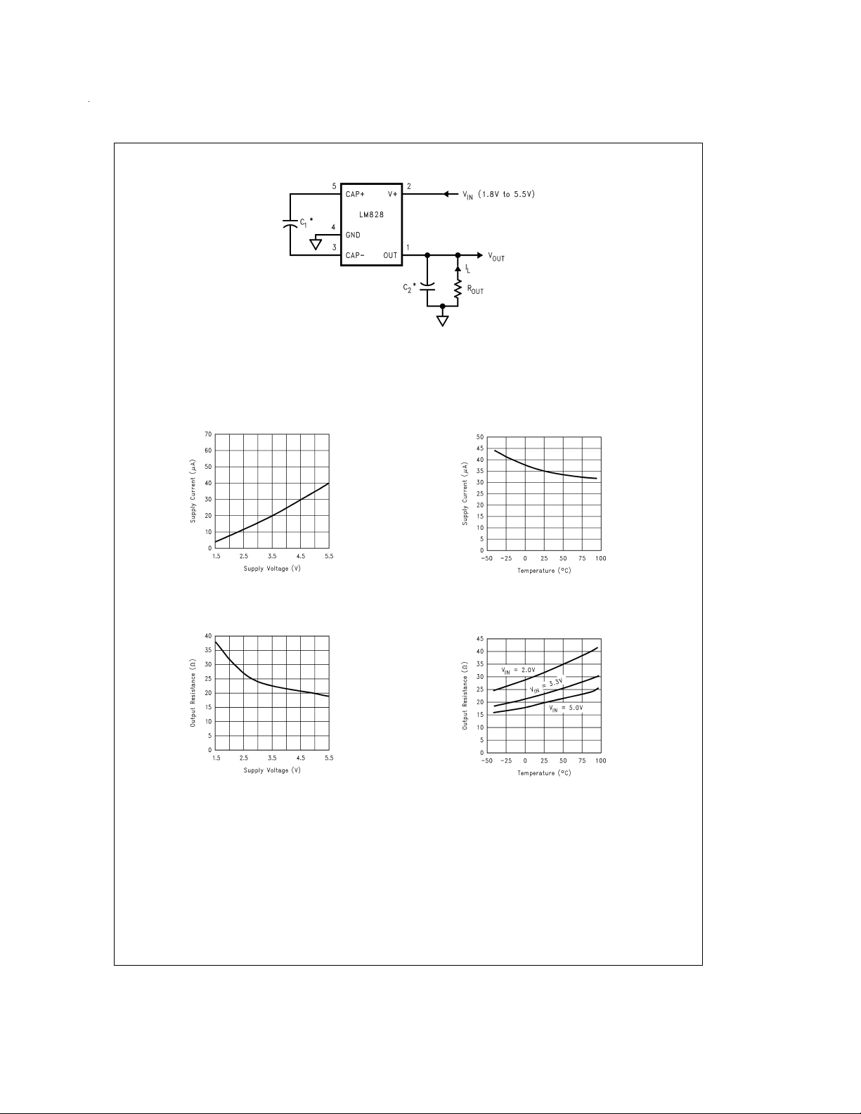
Test Circuit
*
C1and C2are 10 µF capacitors.
FIGURE 1. LM828 Test Circuit
Typical Performance Characteristics
Supply Current vs
Supply Voltage
DS100137-29
Output Source Resistance
vs Supply Voltage
DS100137-3
(Circuit of Figure 1, V+=5V unless otherwise specified)
Supply Current vs
Temperature
DS100137-30
Output Source Resistance
vs Temperature
DS100137-31
DS100137-32
www.national.com3
 Loading...