

NSC LM8272MMX Datasheet
December 2002
LM8272 Dual
RRIO, High Output Current & Unlimited Cap Load Op
Amp in Miniature Package
LM8272 Dual RRIO, High Output Current & Unlimited Cap Load Op Amp in Miniature Package
General Description
The LM8272 is a Rail-to-Rail input and output Op Amp which
can operate with a wide supply voltage range. This device
has high output current drive, greater than Rail-to-Rail input
common mode voltage range, unlimited capacitive load drive
capability while requiring only 0.95mA/channel supply current. It is specifically designed to handle the requirements of
flat panel TFT panel V
being suitable for other low power, and medium speed applications which require ease of use and enhanced performance over existing devices.
Greater than Rail-to-Rail input common mode voltage range
with 50dB of Common Mode Rejection, allows high side and
low side sensing, among many applications, without having
any concerns over exceeding the range and no compromise
in accuracy. Exceptionally wide operating supply voltage
range of 2.5V to 24V alleviates any concerns over functionality under extreme conditions and offers flexibility of use in
multitude of applications. In addition, most device parameters are insensitive to power supply variations; this design
enhancement is yet another step in simplifying its usage.
The LM8272 is offered in the 8-pin MSOP package.
driver applications as well as
COM
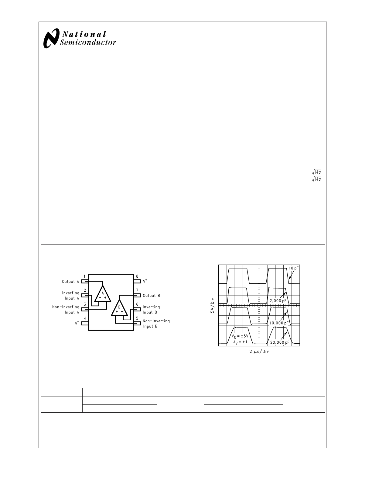
Connection Diagram
8-Pin MSOP
Features
(VS= 12V, TA= 25˚C, Typical values unless specified).
n GBWP 15MHz
n Wide supply voltage range 2.5V to 24V
n Slew rate 15V/µs
n Supply current/channel 0.95mA
n Cap load tolerance Unlimited
n Output short circuit current
n Output current (1V from rails)
n Input common mode voltage 0.3V beyond rails
n Input voltage noise 15nV/
n Input current noise 1.4pA/
±
130mA
±
65mA
Applications
n TFT-LCD flat panel V
n A/D converter buffer
n High side/low side sensing
n Headphone amplifier
Large Signal Step Response for Various Cap. Load
COM
driver
Top View
10130863
10130899
Ordering Information
Package Part Number Package Marking Transport Media NSC Drawing
8-Pin MSOP LM8272MM
LM8272MMX 3.5k Unit Tape and Reel
© 2002 National Semiconductor Corporation DS101308 www.national.com
A60
1k Unit Tape and Reel
MUA08A
Absolute Maximum Ratings (Note 1)
If Military/Aerospace specified devices are required,
please contact the National Semiconductor Sales Office/
Distributors for availability and specifications.
LM8272 Dual
ESD Tolerance
Differential +/−10V
V
IN
Output Short Circuit Duration (Notes 3, 11)
Supply Voltage (V
Voltage at Input/Output pins V
Storage Temperature Range −65˚C to +150˚C
+-V−
) 27V
2KV (Note 2)
200V(Note 9)
+
+0.3V, V−−0.3V
Junction Temperature (Note 4) +150˚C
Soldering Information:
Infrared or Convection (20 sec.) 235˚C
Wave Soldering (10 sec.) 260˚C
Operating Ratings
Supply Voltage (V+-V−) 2.5V to 24V
Junction Temperature Range(Note 4) −40˚C to +85˚C
Package Thermal Resistance, θ
8-Pin MSOP 235C/W
,(Note 4)
JA
5V Electrical Characteristics
Unless otherwise specified, all limited guaranteed for TJ= 25˚C, V+= 5V, V−= 0V, VCM= 0.5V, VO=V+/2, and
>
1MΩ to V−. Boldface limits apply at the temperature extremes.
R
L
Symbol Parameter Condition
V
OS
TC V
Input Offset Voltage VCM= 0.5V & VCM= 4.5V +/−0.7 +/−5
Input Offset Average Drift VCM= 0.5V & VCM= 4.5V
OS
Typ
(Note 5)
+/−2 — µV/˚C
(Note 12)
I
B
I
OS
Input Bias Current (Note 7) —
Input Offset Current 20 250
CMRR Common Mode Rejection Ratio VCMstepped from 0V to 5V 80 64
+
+PSRR Positive Power Supply Rejection Ratio V
from 4.5V to 13V 100 78
CMVR Input Common-Mode Voltage Range CMRR>50dB −0.3 −0.1
5.3 5.1
A
VOL
V
O
I
SC
Large Signal Voltage Gain VO= 0.5 to 4.5V,
= 10kΩ to V+/2
R
L
Output Swing
High
Output Swing
Low
Output Short Circuit Current Sourcing to V
RL= 10kΩ to V
I
SOURCE
R
I
SINK
= 5mA 4.85 4.70
= 10kΩ to V
L
= 5mA 300 350
−
−
+
80 64
4.93 4.85
215 250 mV
100 —
VID= 200mV (Note 10)
Sinking to V
+
100 —
VID= −200mV (Note 10)
I
I
OUT
S
Output Current VID=±200mV, VO= 1V from rails
Supply Current (Both Channel) No load, VCM= 0.5V 1.8 2.3
SR Slew Rate (Note 8) AV= +1, VI=5V
f
u
Unity Gain Frequency VI= 10mVp, RL=2KΩ to V+/2 7.5 — MHz
PP
±
55 — mA
12 — V/µs
GBWP Gain-Bandwidth Product f = 50KHz 13 — MHz
Phi
e
m
n
Phase Margin VI= 10mVp, RL=2kΩ to V+/2 55 — deg
Input-Referred Voltage Noise f = 2KHz, RS=50Ω 15 — nV/
Limit
(Note 6)
+/− 7
±
2.00
±
2.70
400
61
74
0.0
5.0
60
2.8
Units
mV
max
µA
max
nA
max
dB
min
dB
min
V
max
V
min
dB
min
V
min
max
mA
mA
max
www.national.com 2
5V Electrical Characteristics (Continued)
Unless otherwise specified, all limited guaranteed for TJ= 25˚C, V+= 5V, V−= 0V, VCM= 0.5V, VO=V+/2, and
>
1MΩ to V−. Boldface limits apply at the temperature extremes.
R
L
Symbol Parameter Condition
i
n
Input-Referred Current Noise f = 2KHz 1.4 — pA/
Typ
(Note 5)
(Note 6)
Limit
LM8272 Dual
Units
f
max
Full Power Bandwidth ZL= (20pF || 10kΩ)toV+/2 700 — KHz
12V Electrical Characteristics
Unless otherwise specified, all limited guaranteed for TJ= 25˚C, V+= 12V, V−= 0V, VCM= 6V, VO= 6V, and
>
1MΩ to V−. Boldface limits apply at the temperature extremes.
R
L
Symbol Parameter Condition
V
OS
TC V
Input Offset Voltage VCM= 0.5V & VCM= 11.5V +/−0.7 +/−7
Input Offset Average Drift VCM= 0.5V & VCM= 11.5V
OS
Typ
(Note 5)
+/−2 — µV/˚C
(Note 12)
I
B
I
OS
Input Bias Current (Note 7) —
Input Offset Current 30 275
CMRR Common Mode Rejection Ratio VCMstepped from 0V to 12V 88 74
+
+PSRR Positive Power Supply Rejection Ratio V
−PSRR Negative Power Supply Rejection
from 4.5V to 13V, VCM= 0.5V 100 78
85 — dB
Ratio
>
CMVR Input Common-Mode Voltage Range CMRR
50dB −0.3 −0.1
12.3 12.1
A
VOL
V
O
I
SC
Large Signal Voltage Gain VO=1Vto11V
= 10kΩ to V+/2
R
L
Output Swing
High
Output Swing
Low
Output Short Circuit Current Sourcing to V
RL10kΩ to V+/2 11.8 11.7
I
SOURCE
R
I
SINK
= 5mA 11.6 11.5
= 10kΩ to V+/2 0.25 0.3
L
= 5mA .40 .45
−
83 74
130 110
VID= 200mV (Note 10)
Sinking to V
+
130 110
VID= 200mV (Note 10)
I
I
OUT
S
Output Current VID=±200mV, VO= 1V from rails
Supply Current (Both Channel) No load, VCM= 0.5V 1.9 2.4
SR Slew Rate
(Note 8)
R
OUT
f
u
Close Loop Output Resistance AV= +1, f = 100KHz 3 — Ω
Unity Gain Frequency VI= 10mVp, RL=2kΩ to V+/2 8 — MHz
= +1, VI= 10VPP,CL= 10pF 15 —
A
V
A
= +1, VI= 10VPP,CL= 0.1µF 1 —
V
±
65 — mA
GBWP Gain-Bandwidth Product f = 50KHz 15 — MHz
Phi
m
GM Gain Margin V
Phase Margin VI= 10mVp, RL=2kΩ to V+/2 57 — Deg
= 10mVp, RL=2kΩ to V+/2 20 — dB
I
Limit
(Note 6)
+/− 9
±
2.00
±
2.80
550
72
74
0
12.0
70
2.9
Units
mV
max
µA
max
nA
max
dB
min
dB
min
V
max
V
min
dB
min
V
min
V
max
mA
min
mA
max
V/µs
www.national.com3
12V Electrical Characteristics (Continued)
Unless otherwise specified, all limited guaranteed for TJ= 25˚C, V+= 12V, V−= 0V, VCM= 6V, VO= 6V, and
>
1MΩ to V−. Boldface limits apply at the temperature extremes.
R
L
Symbol Parameter Condition
LM8272 Dual
−3dB BW Small Signal -3db Bandwidth A
e
n
Input-Referred Voltage Noise f = 2KHz, RS=50Ω 15 — nV/
= +1, RL=2kΩ to V+/2 12.5 —
V
= +1, RL= 600Ω to V+/2 10.5 —
V
A
= +10, RL= 600Ω to V+/2 1.0 —
V
(Note 5)
Typ
Limit
(Note 6)
Units
MHzA
i
n
f
max
THD+N Total Harmonic Distortion +Noise A
CT Rej. Cross-Talk Rejection f = 5MHz, Driver R
Note 1: Absolute Maximum Ratings indicate limits beyond which damage to the device may occur. Operating Rating indicate conditions for which the device is
intended to be functional, but specific performance is not guaranteed. For guaranteed specifications and the test conditions, see the Electrical Characteristics.
Note 2: Human body model, 1.5kΩ in series with 100pF.
Note 3: Applies to both single-supply and split-supply operation. Continuous short circuit operation at elevated ambient temperature can result in exceeding the
maximum allowed junction temperature of 150˚C.
Note 4: The maximum power dissipation is a function of T
P
D
Note 5: Typical Values represent the most likely parametric norm.
Note 6: All limits are guaranteed by testing or statistical analysis.
Note 7: Positive current corresponds to current flowing into the device.
Note 8: Slew rate is the slower of the rising and falling slew rates. Connected as a Voltage Follower.
Note 9: Machine Model, 0Ω is series with 200pF.
Note 10: Short circuit test is a momentary test. See Note 11.
Note 11: Output short circuit duration is infinite for V
Note 12: Offset voltage average drift determined by dividing the change in V
Input-Referred Current Noise f = 2KHz 1.4 — pA/
Full Power Bandwidth ZL= (20pF || 10kΩ)toV+/2 300 — KHz
= +2, RL=2kΩ to V+/2
V
=8VPP,VS=±5V
V
O
(max), θJA, and TA. The maximum allowable power dissipation at any ambient temperature is
=(TJ(max) - TA)/ θJA. All numbers apply for packages soldered directly onto a PC board.
J
≤ 6V at room temperature and below. For V
S
at temperature extremes into the total temperature change.
OS
= 10kΩ to V+/2 68 — dB
L
>
6V, allowable short circuit duration is 1.5ms.
S
0.02 — %
www.national.com 4
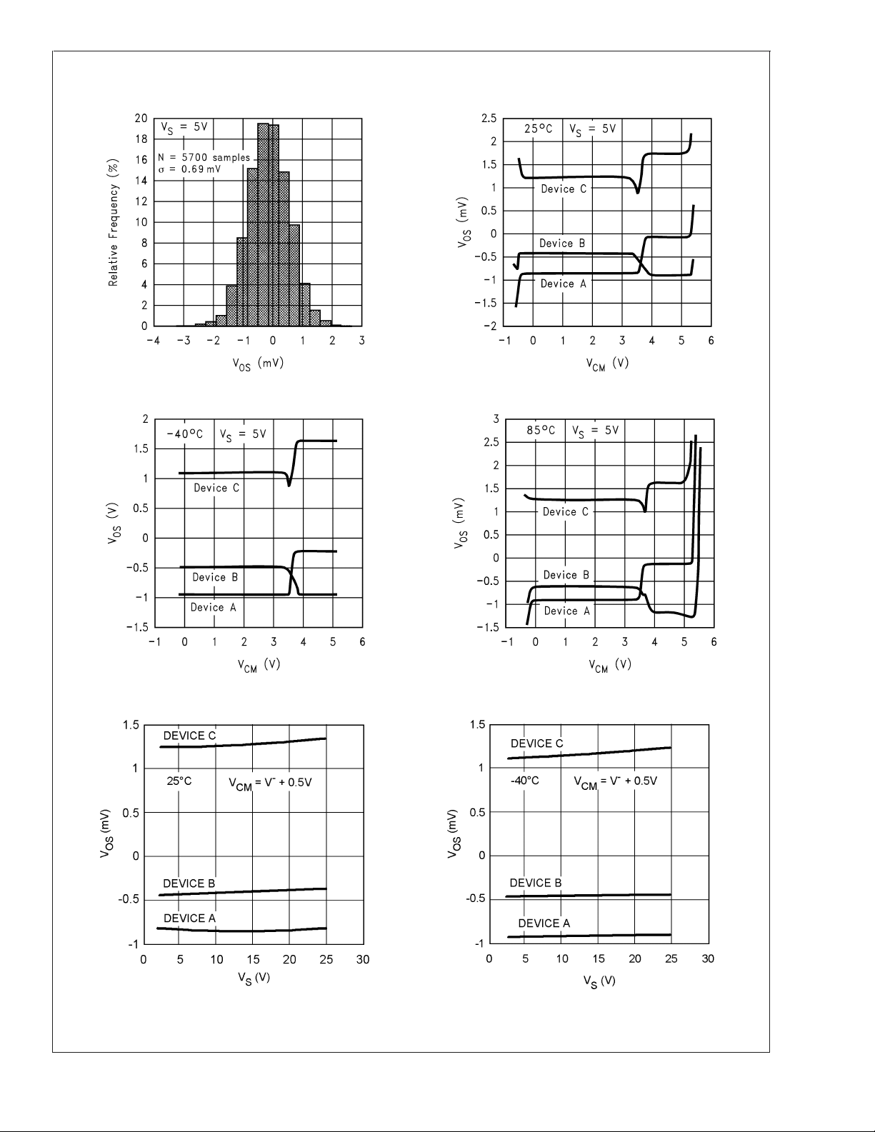
Typical Performance Charateristics
VOSDistribution VOSvs. VCMfor 3 Representative Units
101308A2 10130830
VOSvs. VCMfor 3 Representative Units VOSvs. VCMfor 3 Representative Units
LM8272 Dual
10130829 10130831
VOSvs. VSfor 3 Representative Units VOSvs. VSfor 3 Representative Units
10130884
10130883
www.national.com5
 Loading...