

Page 1
LM78
Microprocessor System Hardware Monitor
LM78 Microprocessor System Hardware Monitor
February 2000
General Description
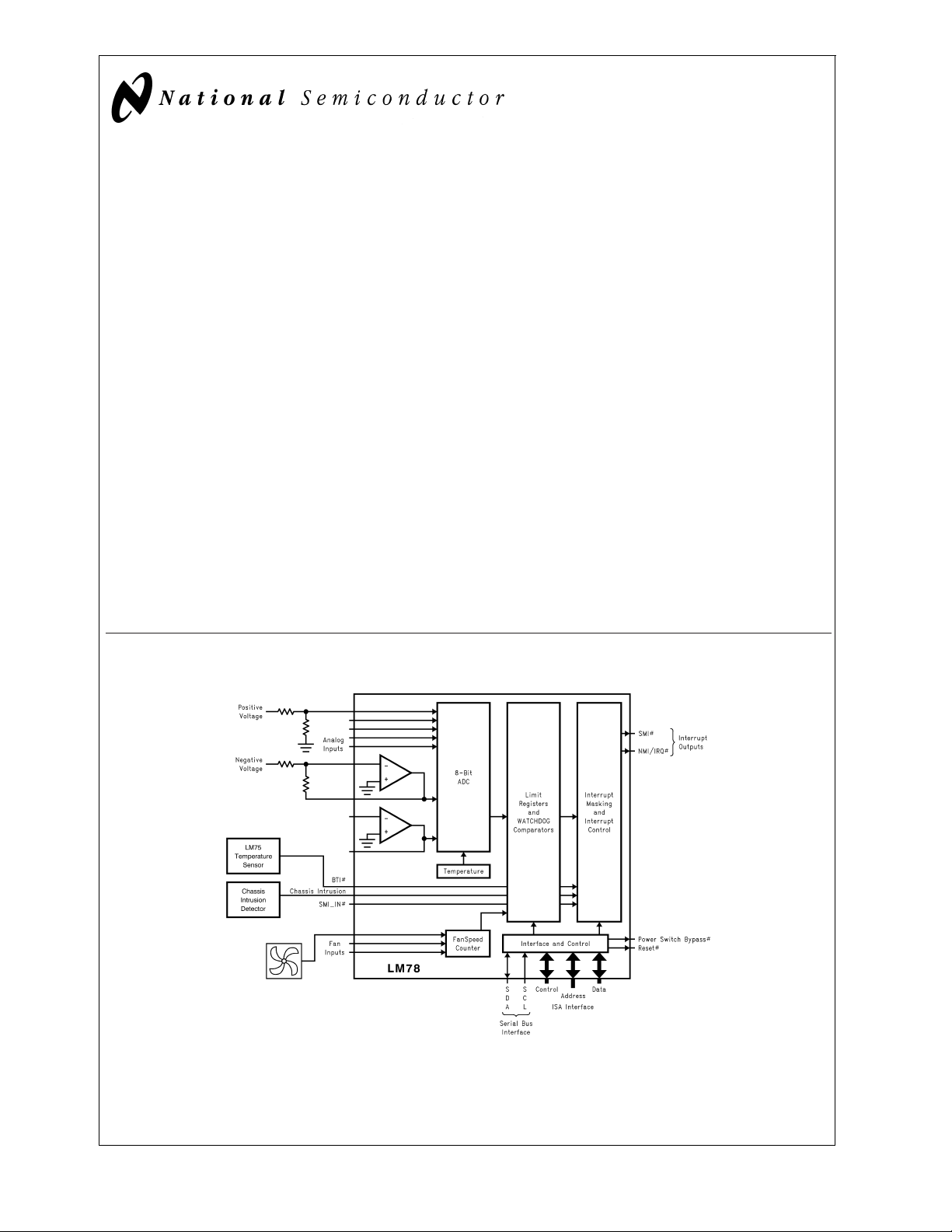
The LM78 is a highly integrated Data Acquisition system for
hardware monitoring of servers, Personal Computers, or
virtually any microprocessor based system. In a PC, the
LM78 can be used to monitor power supply voltages, temperatures, and fan speeds. Actual values for these inputs
can be read at any time, and programmable WATCHDOG
limits in the LM78 activate a fully programmable and
maskable interrupt system with two outputs.
The LM78 has an on-chip temperature sensor, 5 positive
analog inputs, two inverting inputs (for monitoring negative
voltages), and an 8-bit ADC. An input is provided for the
overtemperature outputs of additional temperature sensors
and this is linked to the interrupt system. The LM78 provides
inputs for three fan tachometer outputs. Additional inputs are
provided for Chassis Intrusion detection circuits, VID monitor
inputs, and chainable interrupt. The LM78 provides both ISA
and Serial Bus interfaces. A 32-byte auto-increment RAM is
provided for POST (Power On Self Test) code storage.
Applications
n System Hardware Monitoring for Servers and PCs
n Office Electronics
n Electronic Test Equipment and Instrumentation
Typical Application
Features
n Temperature sensing
n 5 positive voltage inputs
n 2 op amps for negative voltage monitoring
n 3 fan speed monitoring inputs
n Input for additional temperature sensors
n Chassis Intrusion Detector input
n WATCHDOG comparison of all monitored values
n POST code storage RAM
n ISA and I
2
C™Serial Bus interfaces
Key Specifications
j
Voltage monitoring
accuracy
j
Temperature Accuracy
−10˚C to +100˚C
j
Supply Voltage 5V
j
Supply Current Operating: 1 mA typ
Shutdown: 10 µA typ
j
ADC Resolution 8 Bits
±
1% (max)
±
3˚C (max)
DS012873-1
#
indicates Active Low (”Not“)
I2C®is a registered trademark of the Phillips Corporation.
© 2001 National Semiconductor Corporation DS012873 www.national.com
Page 2
Ordering Information
LM78
Temperature Range
−10˚C ≤ T
Order Number Device Marking
LM78CCVF LM78CCVF-J VGZ44A
A
Block Diagram
≤ +100˚C
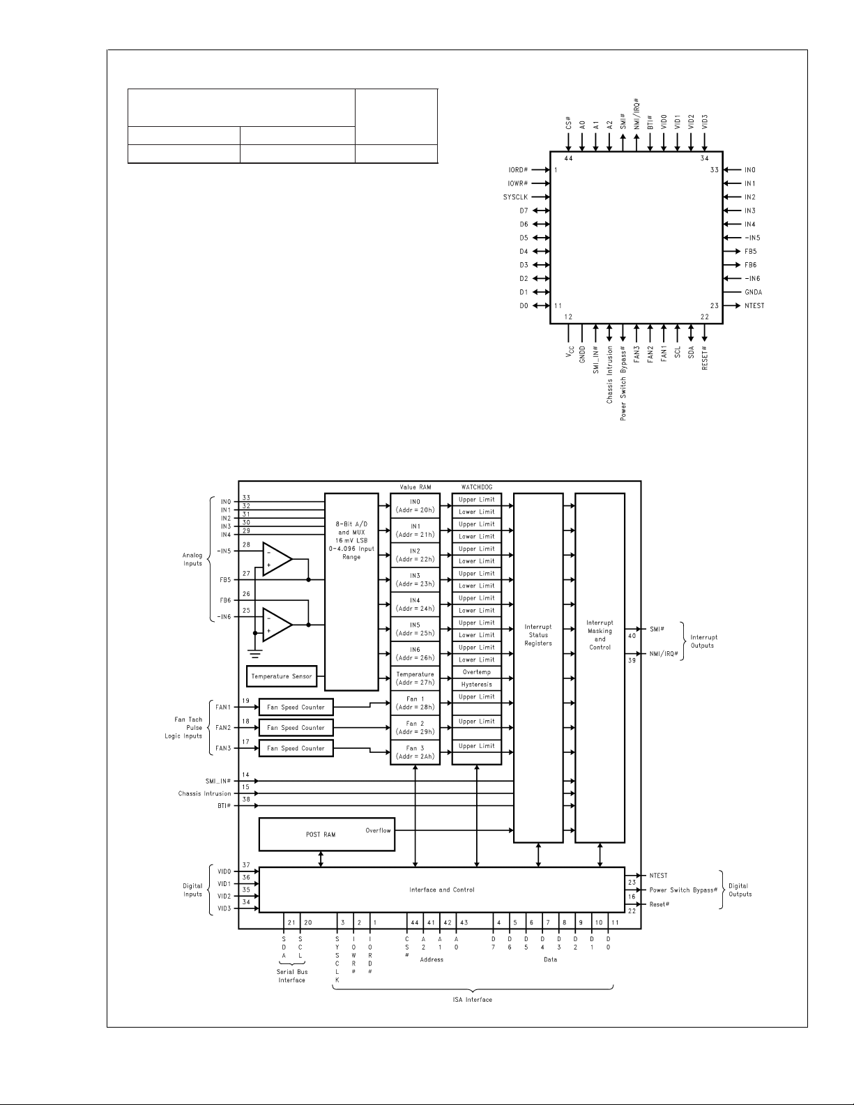
Connection Diagram
Package
DS012873-2
www.national.com 2
DS012873-3
Page 3
Pin Descriptions
LM78
Pin
Name(s)
IORD
IOWR
SYSCLK 3 1 Digital Input The reference clock for the ISA bus. Typically ranges from 4.167 MHz to
D7–D0 4–11 8 Digital I/O Bi-directional ISA bus Data lines. D0 corresponds to the low order bit,
V
(+5V) 12 1 POWER +5V VCCpower. Bypass with the parallel combination of 10 µF
CC
GNDD 13 1 GROUND Internally connected to all digital circuitry.
SMI__IN
Chassis
Intrusion
Power
Switch
Bypass
FAN3–FAN1 17–19 3 Digital Input 0V to +5V amplitude fan tachometer input.
SCL 20 1 Digital Input Serial Bus Clock.
SDA 21 1 Digital I/O Serial Bus bidirectional Data.
RESET
NTEST 23 1 Test Output NAND Tree totem-pole output that provides board-level connectivity
GNDA 24 1 GROUND Internally connected to all analog circuitry. The ground reference for all
−IN6 25 1 Analog Input Ground-referred inverting op amp input. Refer to Section 4.0, “ANALOG
FB6 26 1 Analog Output Output of inverting op amp for Input 6. Refer to section 4.0, “ANALOG
FB5 27 1 Analog Output Output of inverting op amp for Input 5. Refer to section 4.0, “ANALOG
−IN5 28 1 Analog Input Ground-referred inverting op amp input. Refer to Section 4.0, “ANALOG
IN4–IN0 29–33 5 Analog Input 0V to 4.096V FSR Analog Inputs.
VID3–VID0 34–37 4 Digital Input Voltage Supply readouts from P6. This value is read in the VID/Fan
BTI
NMI/IRQ
SMI 40 1 Digital Output System Management Interrupt (open drain). This output is enabled when
Pin
Number
1 1 Digital Input An active low standard ISA bus I/O Read Control.
2 1 Digital Input An active low standard ISA bus I/O Write Control.
14 1 Digital Input Chainable SMI (System Management Interrupt) Input. This is an active
15 1 Digital I/O An active high input from an external circuit which latches a Chassis
16 1 Digital Output An active low push-pull output intended to drive an external P-channel
22 1 Digital Output Master Reset, 5 mA driver (open drain), active low output with a 20 ms
38 1 Digital Input Board Temperature Interrupt driven by O.S. outputs of additional
39 1 Digital Output Non-Maskable Interrupt (open source)/Interrupt Request (open drain).
Number
of Pins
Type Description
8.33 MHz. The minimum clock frequency this input can handle is 1 Hz.
with D7 the high order bit.
(electolytic or tantalum) and 0.1 µF (ceramic) bypass capacitors.
low input that propagates the SMI signal to the SMI output of the LM78
via SMI Mask Register Bit 6 and SMI enable Bit 1 of the Configuration
Register.
Intrusion event. This line can go high without any clamping action
regardless of the powered state of the LM78. The LM78 provides an
internal open drain on this line, controlled by Bit 7 of NMI Mask Register
2, to provide a minimum 20 ms reset of this line.
power MOSFET for software power control.
minimum pulse width. Available when enabeld via Bit 7 in SMI Mask
Register 2.
testing. Refer to Section 11.0 on NAND Tree testing.
analog inputs.
INPUTS”.
INPUTS”.
INPUTS”.
INPUTS”.
Divisor Register.
temperature sensors such as LM75. Provides internal pull-up of 10 kΩ.
The mode is selected with Bit 5 of the Configuration Register and the
output is enabled when Bit 2 of the Configuration Register is set to 1.
The default state is disabled and IRQ mode.
Bit 1 in the Configuration Register is set to 1. The default state is
disabled.
www.national.com3
Page 4

Pin Descriptions (Continued)
LM78
Pin
Name(s)
A2–A0 41–43 3 Digital Input The three lowest order bits of the 16-bit ISA Address Bus. A0
CS
TOTAL PINS 44
Pin
Number
44 1 Digital Input Chip Select input from an external decoder which decodes high order
Number
of Pins
Type Description
corresponds to the lowest order bit.
address bits on the ISA Address Bus. This is an active low input.
www.national.com 4
Page 5
LM78
Absolute Maximum Ratings (Notes 1, 2)
If Military/Aerospace specified devices are required,
please contact the National Semiconductor Sales Office/
Vapor Phase (60 seconds) 215˚C
Infrared (15 seconds) 220˚C
Storage Temperature −65˚C to +150˚C
Distributors for availability and specifications.
Positive Supply Voltage (V
Voltage on Any Input or Output Pin −0.3V to (V
Ground Difference (GNDD–GNDA)
Input Current at any Pin (Note 3)
Package Input Current (Note 3)
) 6.5V
CC
CC
±
300 mV
±
±
Maximum Junction Temperature
max) 150˚C
(T
J
ESD Susceptibility(Note 5)
Human Body Model 2000V
Machine Model 175V
Soldering Information
+0.3V)
5mA
20 mA
Operating Ratings(Notes 1, 2)
Operating Temperature Range T
LM78 −55˚C ≤ TA≤ +125˚C
Specified Temperature Range T
LM78 −10˚C ≤ TA≤ +100˚C
Junction to Ambient Thermal Resistance (θ
NS Package ID: VGZ44A 62˚C/W
Supply Voltage (V
) +4.25V to +5.75V
CC
Ground Difference
(IGNDD–GNDAI) ≤100 mV
Voltage Range −0.05V to VCC+ 0.05V
V
IN
≤ TA≤ T
MIN
≤ TA≤ T
MIN
(Note 4) )
JA
PQFP Package (Note 6) :
DC Electrical Characteristics(Note 7)
The following specifications apply for +4.25 VDC≤VCC≤ +5.75 VDC,f
fied. Boldface limits apply for T
A=TJ=TMIN
to T
; all other limits TA=TJ= 25˚C.
MAX
Symbol Parameter Conditions Typical Limits Units
POWER SUPPLY CHARACTERISTICS
I
CC
Supply Current Interface Inactive 1.0 2 mA (max)
Shutdown Mode 10 µA
TEMPERATURE-TO-DIGITAL CONVERTER CHARACTERISTICS
Accuracy −10˚C ≤ T
A
Resolution 1 ˚C (min)
ANALOG-TO-DIGITAL CONVERTER CHARACTERISTICS
Resolution (8 bits with full-scale at 4.096V) 16 mV
TUE Total Unadjusted Error (Note 10)
DNL Differential Non-Linearity
PSS Power Supply Sensitivity
t
C
Total Monitoring Cycle Time (Note 11) 1.0 1.5 sec (max)
OP AMP CHARACTERISTICS
Output Current (Sourcing) 50 µA
Input Offset Voltage I
OUT
=50µA
Input Bias Current
PSRR 60 dB
DC Open Loop Gain 70 dB
Gain Bandwidth Product 500 kHz
MULTIPLEXER/ADC INPUT CHARACTERISTICS
On Resistance 400 2000 Ω (max)
Off Channel Leakage Current
Input Current (On Channel Leakage Current)
FAN RPM-TO-DIGITAL CONVERTER
Accuracy +25˚C ≤ T
−10˚C ≤ T
A
A
Full-scale Count 255 (max)
= 8.33 MHz, RS=25Ω, unless otherwise speci-
SYSCLK
(Note 8) (Note 9) (Limits)
≤ +100˚C
±
1 %/V
±
1mV
±
0.1 nA
±
0.1 nA
±
0.1 nA
≤ +75˚C
≤ +100˚C
±
3 ˚C (max)
±
1 % (max)
±
1 LSB
±
10 % (max)
±
15 % (max)
MAX
MAX
www.national.com5
Page 6
DC Electrical Characteristics(Note 7) (Continued)
LM78
The following specifications apply for +4.25 VDC≤VCC≤ +5.75 VDC,f
fied. Boldface limits apply for T
A=TJ=TMIN
to T
; all other limits TA=TJ= 25˚C.
MAX
= 8.33 MHz, RS=25Ω, unless otherwise speci-
SYSCLK
Symbol Parameter Conditions Typical Limits Units
(Note 8) (Note 9) (Limits)
FAN RPM-TO-DIGITAL CONVERTER
FAN1 and FAN2 Nominal Input
RPM (See Section 6.0)
Divisor = 1, Fan Count = 153
(Note 12)
Divisor = 2, Fan Count = 153
8800 RPM
4400 RPM
(Note 12)
Divisor = 3, Fan Count = 153
2200 RPM
(Note 12)
Divisor = 4, Fan Count = 153
1100 RPM
(Note 12)
FAN3 Design Nominal Input RPM Fan Count = 153 (Note 12) 4400 RPM
Internal Clock Frequency +25˚C ≤ T
≤ +75˚C 22.5 20.2 kHz (min)
A
24.8 kHz (max)
−10˚C ≤ T
≤ +100˚C 22.5 19.1 kHz (min)
A
25.9 kHz (max)
DIGITAL OUTPUTS (Power Switch Bypass, NTEST, NMI/IRQ)
V
V
OUT(1)
OUT(0)
Logical “1” Output Voltage I
Logical “0” Output Voltage I
=±5.0 mA 2.4 V (min)
OUT
=±5.0 mA 0.4 V (max)
OUT
ISA D0–D7 DIGITAL OUTPUTS
V
V
I
OUT
OUT(1)
OUT(0)
Logical “1” Output Voltage I
Logical “0” Output Voltage I
TRI-STATE®Output Current V
=±12.0 mA 2.4 V (min)
OUT
=±12.0 mA 0.4 V (max)
OUT
=0V
OUT
V
OUT
=V
DC
CC
0.005 1 µA (max)
−0.005 −1 µA (min)
OPEN DRAIN DIGITAL OUTPUTS (SDA, RESET, SMI, Chassis Intrusion)
V
I
OH
OUT(0)
Logical “0” Output Voltage I
High Level Output Current V
RESET and Chassis Intrusion
= −5.0 mA 0.4 V (min)
OUT
OUT
=V
CC
0.1 100 µA (max)
45 20 ms (min)
Pulse Width
DIGITAL INPUTS: SMI__IN, VID0–VID3, BTI, CS, A0, A1, A2, Mode Control and Interface Inputs (IORD, IOWR, SYSCLK),
Data Lines (D0–D7), Chassis Intrusion, and Tach Pulse Logic Inputs (FAN1, FAN2, FAN3)
V
IN(1)
V
IN(0)
Logical “1” Input Voltage 2.0 V (min)
Logical “0” Input Voltage 0.8 V (max)
SERIAL BUS DIGITAL INPUTS (SCL, SDA)
V
IN(1)
V
IN(0)
Logical “1” Input Voltage 0.7xV
Logical “0” Input Voltage 0.3xV
CC
CC
ALL DIGITAL INPUTS EXCEPT FOR BTI
I
I
C
IN(1)
IN(0)
IN
Logical “1” Input Current VIN=V
CC
Logical “0” Input Current VIN=0V
DC
−0.005 −1 µA (min)
0.005 1 µA (max)
Digital Input Capacitance 20 pF
BIT DIGITAL INPUT
I
I
C
IN(1)
IN(0)
IN
Logical “1” Input Current VIN=V
CC
Logical “0” Input Current VIN=0V
DC
1 10 µA (max)
−500 −2000 µA (max)
Digital Input Capacitance 20 pF
V (min)
V (max)
www.national.com 6
Page 7
LM78
AC Electrical Characteristics(Note 13) The following specifications apply for +4.25 V
+5.75 V
unless otherwise specified. Boldface limits apply for TA=TJ=T
DC
MIN
to T
; all other limits TA=TJ=
MAX
DC
≤ VCC≤
25˚C.
Symbol Parameter Conditions Typical Limits Units
(Note 8) (Note 9) (Limits)
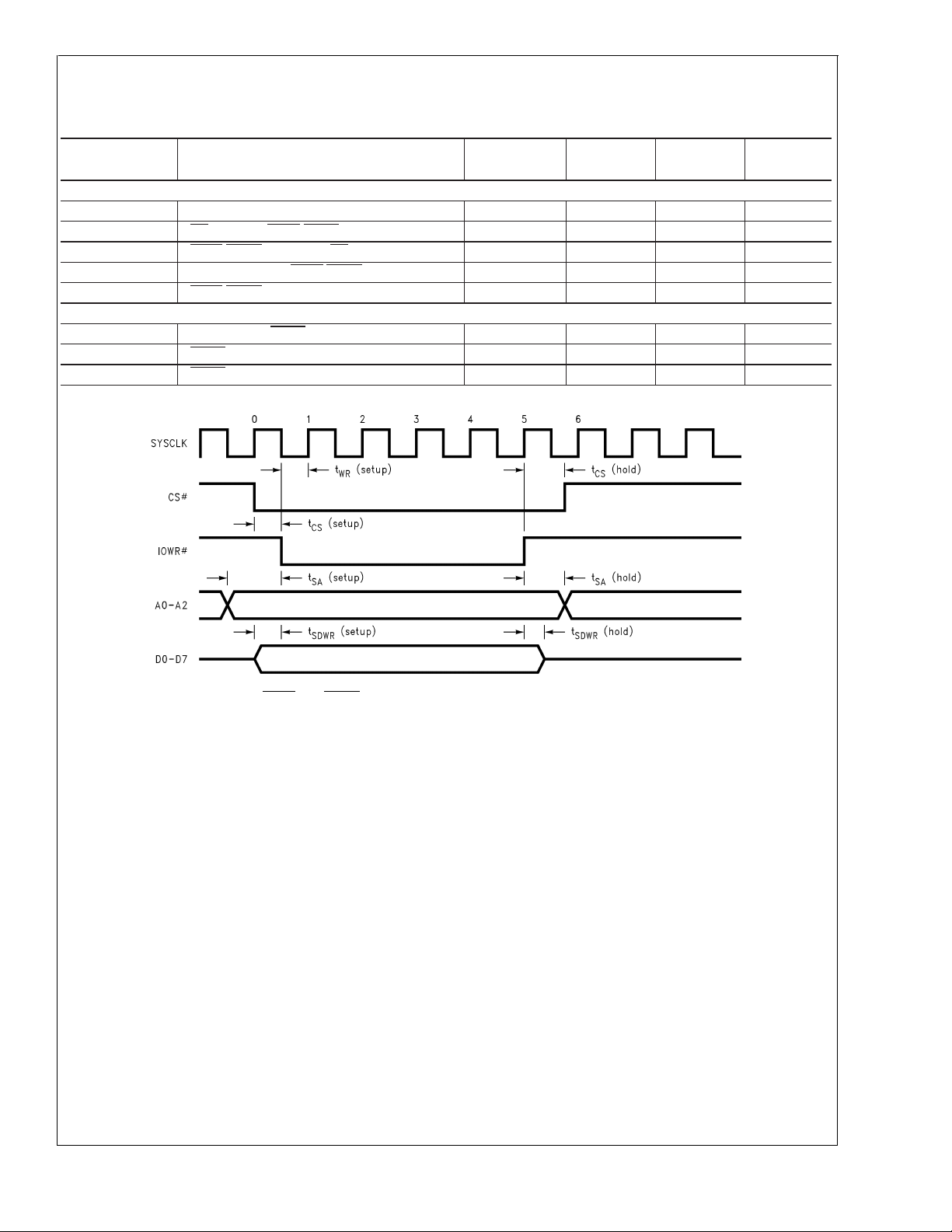
ISA TIMING CHARACTERISTICS
f
SYSCLK
t
(setup) CS Active to IORD/IOWR Active 10 ns (min)
CS
t
(hold) IORD/IOWR Inactive to CS Inactive 10 ns (min)
CS
t
(setup) Address Valid to IORD/IOWR Active 30 ns (min)
SA
t
(hold) IORD/IOWR Inactive to Address Invalid 10 ns (min)
SA
System Clock (SYSCLK) Input Frequency 8.33 MHz
ISA WRITE TIMING
t
(setup) Data Valid to IOWR Active 5 ns (min)
SDWR
t
(hold) IOWR Inactive to Data Invalid 5 ns (min)
SDWR
t
(setup) IOWR Active to Rising Edge of SYSCLK 20 ns (min)
WR
DS012873-4
The delay between consecutive IORD and IOWR pulses should be greater than 50 ns to ensure that an Power-on reset does not
occur unintentionally. (See Section 3.2 ‘Resets’ )
FIGURE 1. ISA Bus Write Timing Diagram
www.national.com7
Page 8
AC Electrical Characteristics(Note 13) The following specifications apply for +4.25 V
LM78
unless otherwise specified. Boldface limits apply for TA=TJ=T
MIN
to T
; all other limits TA=TJ= 25˚C. (Continued)
MAX
≤ VCC≤ +5.75 V
DC
Symbol Parameter Conditions Typical Limits Units
(Note 8) (Note 9) (Limits)
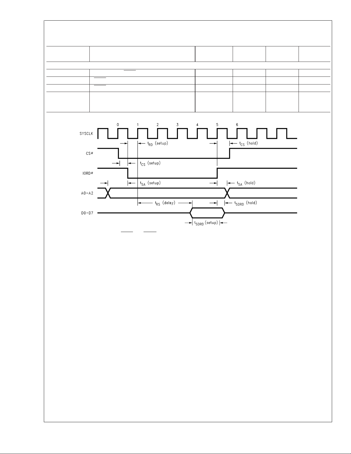
ISA READ TIMING
t
(setup) Data Valid to IORD Inactive 120 ns (min)
SDRD
t
(hold) IORD Inactive to Data Invalid 5 ns (min)
SDRD
t
(setup) IORD Active to Rising Edge of SYSCLK 20 ns (min)
RD
t
(delay) Rising Edge of SYSCLK number 1 to Data
RS
Valid
With 8.33
MHz
360 ns (max)
SYSCLK
DC
DS012873-5
The delay between consecutive IORD and IOWR pulses should be greater than 50 ns to ensure that an Power-on reset does not
occur unintentionally. (SeeSection 3.2‘Resets’ )
FIGURE 2. ISA Bus Read Timing Diagram
www.national.com 8
Page 9
LM78
AC Electrical Characteristics(Note 13) The following specifications apply for +4.25 V
unless otherwise specified. Boldface limits apply for TA=TJ=T
MIN
to T
; all other limits TA=TJ= 25˚C. (Continued)
MAX
≤ VCC≤ +5.75 V
DC
Symbol Parameter Conditions Typical Limits Units
(Note 8) (Note 9) (Limits)
SERIAL BUS TIMING CHARACTERISTICS
t
1
t
2
t
3
t
4
t
5
SCL (Clock) Period 2.5 µs (min)
Data In Setup Time to SCL High 100 ns (min)
Data Out Stable After SCL Low 0 ns (min)
SDA Low Setup Time to SCL Low (start) 100 ns (min)
SDA High Hold Time After SCL High (stop) 100 ns (min)
DS012873-6
FIGURE 3. Serial Bus Timing Diagram
DC
www.national.com9
Page 10
Electrical Characteristics (Continued)
LM78
Note 1: Absolute Maximum Ratings indicate limits beyond which damage to the device may occur. Operating Ratings indicate conditions for which the device is
functional, but do not guarantee specific performance limits. For guaranteed specifications and test conditions, see the Electrical Characteristics. The guaranteed
specifications apply only for the test conditions listed. Some performance characteristics may degrade when the device is not operated under the listed test
conditions.
Note 2: All voltages are measured with respect to GND, unless otherwise specified
Note 3: When the input voltage (V
The 20 mA maximum package input current rating limits the number of pins that can safely exceed the power supplies with an input current of 5 mA to four.
Note 4: The maximum power dissipation must be derated at elevated temperatures and is dictated by T
allowable power dissipation at any temperature is P
Note 5: The human body model is a 100 pF capacitor discharged through a 1.5 kΩ resistor into each pin. The machine model is a 200 pF capacitor discharged
directly into each pin.
Note 6: See the section titled “Surface Mount” found in any post 1986 National Semiconductor Linear Data Book for other methods of soldering surface mount
devices.
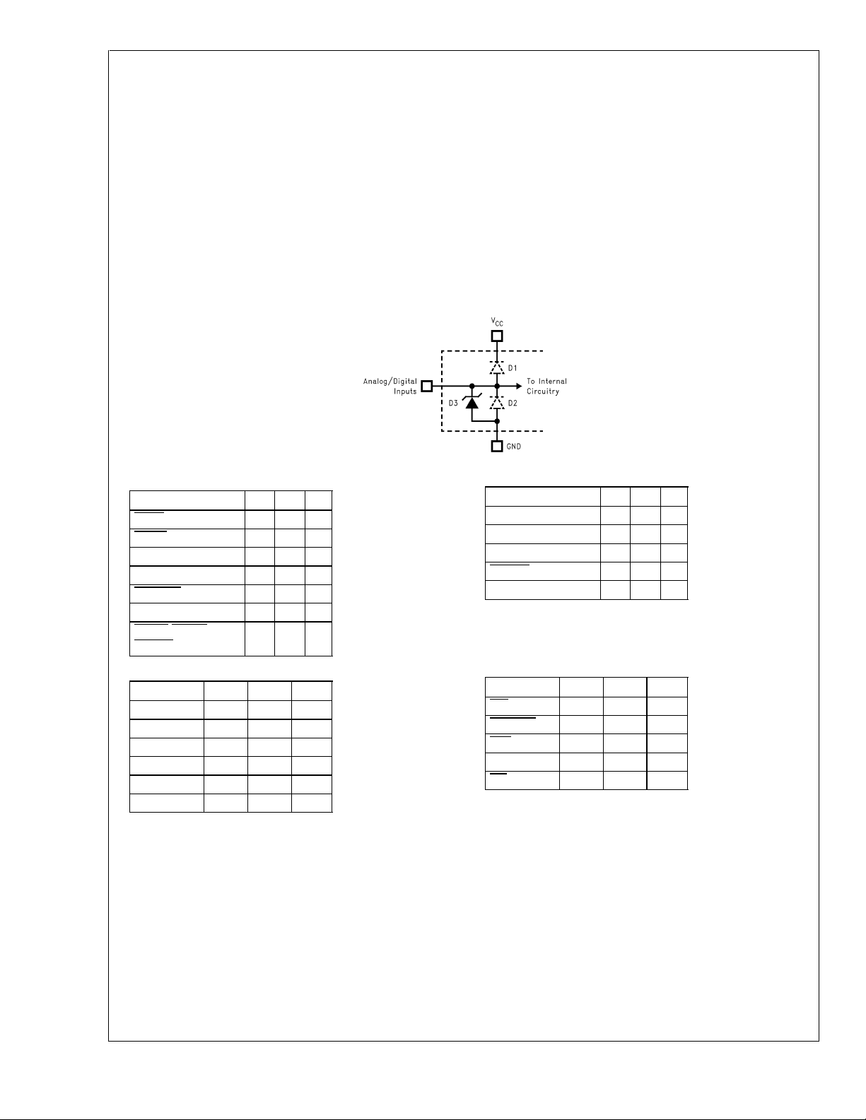
Note 7: Each input and output is protected by a nominal 6.5V breakdown voltage zener diode to GND; as shown below, input voltage magnitude up to 0.3V above
V
or 0.3V below GND will not damage the LM78. There are parasitic diodes that exist between the inputs and the power supply rails. Errors in the ADC conversion
CC
can occur if these diodes are forward biased by more than 50 mV. As an example, if V
conversions.
An x indicates that the diode exists.
) at any pin exceeds the power supplies (V
IN
=(TJmax−TA)/θJA.
D
<
(GNDD or GNDA) or V
IN
is 4.50 VDC, input voltage must be ≤ 4.55 VDC, to ensure accurate
CC
DS012873-7
>
VCC), the current at that pin should be limited to 5 mA.
IN
max, θJAand the ambient temperature, TA. The maximum
J
Pin Name D1 D2 D3
IORD
IOWR
x
x
SYSCLK x
D0–D7 xxx
SMI__IN
x
Pin Name D1 D2 D3
FAN1–FAN3 x
SCL x
SDA x x
RESET
xx
NTEST x x x
Chassis Intrusion x x
Power Switch
xxx
Bypass
Pin Name D1 D2 D3
−IN6 x x
FB6 x x x
FB5 x x x
−IN5 x x
IN4–IN0 x x x
Pin Name D1 D2 D3
BTI
NMI/IRQ
SMI
xx
xxx
xx
A0–A2 x
CS
x
VID3–VID0 x x x
FIGURE 4. ESD Protection Input Structure
Note 8: Typicals are at T
Note 9: Limits are guaranteed to National’s AOQL (Average Outgoing Quality Level).
Note 10: TUE (Total Unadjusted Error) includes Offset, Gain and Linearity errors of the ADC and any error introduced by the amplifiers as shown in the circuit of
Figure 13
Note 11: TotalMonitoring Cycle Time includes temperature conversion, 7 analog input voltage conversions and 3 tachometer readings. Each temperature and input
voltage conversion takes 100 ms typical and 112 ms maximum. Fan tachometer readings take 20 ms typical, at 4400 rpm, and 200 ms max.
Note 12: The total fan count is based on 2 pulses per revolution of the fan tachometer output.
Note 13: Timing specifications are tested at the TTL logic levels, V
to 1.4V.
.
=25˚C and represent most likely parametric norm.
J=TA
IL
=0.4V for a falling edge and VIH=2.4V for a rising edge. TRI-STATE output voltage is forced
www.national.com 10
Page 11

Test Circuit
FIGURE 5. Digital Output Load Circuitry
Functional Description
1.0 GENERAL DESCRIPTION
The LM78 provides 7 analog inputs, a temperature sensor, a
Delta-Sigma ADC (Analog-to-Digital Converter), 3 fan speed
counters, WATCHDOGregisters, and a variety of inputs and
outputs on a single chip. Interfaces are provided for both the
ISA parallel bus or Serial Bus. The LM78 performs power
supply, temperature, and fan monitoring for personal computers.
The LM78 continuously converts analog inputs to 8-bit digital
words with a 16 mV LSB (Least Significant Bit) weighting,
yielding input ranges of from 0V to 4.096V.The two negative
analog inputs provide inverting op amps, with their
non-inverting input referred to ground. With additional external feedback components, these inputs provide measurements of negative voltages (such as -5V and -12V power
supplies). The analog inputs are useful for monitoring several power supplies present in a typical computer. Temperature is converted to an 8-bit two’s-complement digital word
with a 1˚C LSB.
Fan inputs measure the period of tachometer pulses from
the fans, providing a higher count for lower fan speeds. The
fan inputs are digital inputs with an acceptable range of 0V to
5V and a transition level of approximately 1.4V. Full scale fan
counts are 255 (8-bit counter) and this represents a stopped
or very slow fan. Nominal speeds, based on a count of 153,
are programmable from 1100 to 8800 RPM on FAN1 and
FAN2, with FAN3 fixed at 4400 RPM. Signal conditioning
circuitry is included to accommodate slow rise and fall times.
The LM78 provides a number of internal registers, as detailed in
•
•
•
•
Figure 6
Configuration Register: Provides control and configuration.
Interrupt Status Registers: Two registers to provide
status of each WATCHDOG limit or Interrupt event.
Interrupt Mask Registers: Allows masking of individual Interrupt sources, as well as separate masking for
each of both hardware Interrupt outputs.
VID/Fan Divisor Registers: A register to read the status of the VID input lines. The high bits of this register
contain the divisor bits for FAN1 and FAN2 inputs.
. These include:
DS012873-8
Serial Bus Address Register: Contains the Serial Bus
•
address. At power on it assumes the default value of
0101101 binary, and can be altered via the ISA or Serial
Bus interface.
Chip Reset/ID Register: Allows reseting of all the reg-
•
isters to the default power-on reset value. Provides a bit
for identification between the current version of this device and an older version which does not have this reset
capability.
POST RAM: FIFO RAM to store up to 32 bytes of 8-bit
•
POST codes. Overflow of the POST RAM will set an
Interrupt. The POST RAM, located at base address x0h
and x4h, allows for easy decoding to address 80h and
84h, the normal addresses for outputting of POST codes.
Interrupt will only be set when writing to port x0h or x4h.
The POST RAM can be read via ports 85h and 86h.
Value RAM: The monitoring results: temperature, volt-
•
ages, fan counts, and WATCHDOG limits are all contained in the Value RAM. The Value RAM consists of a
total of 64 bytes. The first 11 bytes are all of the results,
the next 19 bytes are the WATCHDOG limits, and are
located at 20h-3Fh, including two unused bytes in the
upper locations. The next 32 bytes, located at 60h-7Fh,
mirror the first 32 bytes with identical contents. The only
difference in the upper bytes are that they auto-increment
the LM78 Internal Address Register when read from or
written to via the ISA bus (auto-increment is not available
for Serial Bus communications).
When the LM78 is started, it cycles through each measurement in sequence, and it continuously loops through the
sequence approximately once every second. Each measured value is compared to values stored in WATCHDOG, or
Limit registers. When the measured value violates the programmed limit the LM78 will set a corresponding Interrupt in
the Interrupt Status Registers. Two hardware Interrupt lines,
SMI and NMI/IRQ, are fully programmable with separate
masking of each Interrupt source, and masking of each
output. In addition, the Configuration Register has control
bits to enable or disable the hardware Interrupts.
Additional digital inputs are provided for chaining of SMI
(System Management Interrupt), outputs of multiple external
LM75 temperature sensors via the BTI (Board Temperature
Interrupt) input, and a Chassis Intrusion input. The Chassis
Intrusion input is designed to accept an active high signal
from an external circuit that latches when the case is removed from the computer.
LM78
www.national.com11
Page 12

Functional Description (Continued)
LM78
2.0 INTERFACE
The LM78 only decodes the three lowest address bits on the
ISA bus. Referring to the ISA bus timing diagrams in
1
and
Figure 2
low by external address decoder circuitry to access the
LM78. The LM78 decodes the following base addresses:
-Port x0h: Power On Self Test codes from ISA bus.
-Port x4h: Power On Self Test codes from ISA bus.
-Port x5h: The LM78s Internal Address Register
-Port x6h: Data Register
IORD is the standard ISA bus signal that indicates to the
LM78 that it may drive data on to the ISA data bus.
IOWR is the standard ISA command to the LM78 that it may
latch data from the ISA bus.
SYSCLK is the standard ISA SYSCLK, typically 8.33 MHz.
This clock is used only for timing of the ISA interface of the
LM78.All other clock functions within LM78 such as the ADC
and fan counters are done with a separate asynchronous
internal clock.
, the Chip Select Input, CS, should be taken
Figure
A typical application designed to utilize the POST RAM
would decode the LM78 to the address space starting at
80h, which is where POST codes are output to. Otherwise,
the LM78 can be decoded into a different desired address
space.
To communicate with an LM78 Register, first write the address of that Register to Port x5h. Read or write data from or
to that register via Port x6h. A write will take IOWR low, while
a read will take IORD low.
If the Serial Bus Interface and ISA bus interface are used
simultaneously there is the possibility of collision. To prevent
this from occurring in applications where both interfaces are
used, read port x5h and if the Most Significant Bit, D7, is
high, ISA communication is limited to reading port x5h only
until this bit is low. A Serial Bus communication occurring
while ISA is active will not be a problem, since even a single
bit of Serial Bus communication requires 10 microseconds,
in comparison to less than a microsecond for an entire ISA
communication.
www.national.com 12
Page 13

Functional Description (Continued)
LM78
FIGURE 6. LM78 Register Structure
DS012873-9
www.national.com13
Page 14

Functional Description (Continued)
LM78
2.1 Internal Registers of the LM78
TABLE 1. The internal registers and their corresponding internal LM78 address is as follows:
Register LM78 Internal Hex
Address
(This is the data to be
written to Port x5h)
Configuration Register 40h 0000 1000
Interrupt Status Register 1 41h 0000 0000 Auto-increment to the address of Interrupt Status
Interrupt Status Register 2 42h 0000 0000
SMI Mask Register 1
SMI Mask Register 2
NMI Mask Register 1 45h 0000 0000 Auto-increment to the address of NMI Mask
NMI Mask Register 2 46h 0100 0000
VID/Fan Divisor Register 47h 0101 XXXX The first four bits set the divisor for Fan
Serial Bus Address Register 48h 0010 1101
Chip Reset/ID Register 49h 0100 0000
POST RAM 00h-1Fh Auto-increment when written to from Port x0h or
Value RAM 20h-3Fh
Value RAM 60h-7Fh Auto-increment after a read or write to Port x6h.
A typical communication with the LM78 would consist of:
1. Write to Port x5h the LM78 Internal Address (from column 2 above) of the desired register. Alternatively,when
both ISA and Serial Bus interfaces are used, the first
step in a communication may be to read Port x5h to
ascertain the state of the Busy bit to avoid contention
with an Serial Bus communication.
The LM78 Internal Address latches, and does not have to be written if it is already pointing at the desired register. The LM78
Internal Address Register is read/write (Bit 7 is read only).
43h 0000 0000 Auto-increment to the address of SMI Mask
44h 0000 0000
Power on
Value
Register 2 after a read or write to Port x6h.
Register 2 after a read or write to Port x6h.
Register 2 after a read or write to Port x6h.
Counters 1 and 2. The lower four bits reflect the
state of the VID inputs.
x4h. Auto-increment after a read or write to Port
x6h, with a separate pointer. Auto-incrementing
stops when address 1Fh is reached.
Auto-incrementing stops when address 7Fh is
reached.
2. Read or write the corresponding registers data with
reads/writes from Port x6h.
Notes
www.national.com 14
Page 15

Functional Description (Continued)
2.2 Serial Bus Interface
(a) Serial Bus Write to the Internal Address Register followed by the Data Byte
LM78
DS012873-10
(b) Serial Bus Write to the Internal Address Register Only
(c) Serial Bus Read from a Register with the Internal Address Register Preset to Desired Location
FIGURE 7. Serial Bus Timing
When using the Serial Bus Interface a write will always
consist of the LM78 Serial Bus Interface Address byte, followed by the Internal Address Register byte, then the data
byte. There are two cases for a read:
1. If the Internal Address Register is known to be at the
desired Address, simply read the LM78 with the Serial
Bus Interface Address byte, followed by the data byte
read from the LM78.
2. If the Internal Address Register value is unknown, write
to the LM78 with the Serial Bus Interface Address byte,
followed by the Internal Address Register byte. Then
restart the Serial Communication with a Read consisting
of the Serial Bus Interface Address byte, followed by the
data byte read from the LM78.
In all other respects the LM78 functions identically for Serial
Bus communications as it does for ISA communications.
DS012873-11
DS012873-12
Auto-Increment does not operate. When writing to or reading
from a Register which Auto-Increments with ISA communications, the Register must be manually incremented for
Serial Bus communications.
The default power on Serial Bus address for the LM78 is:
0101101binary.This address can be changed by writing any
desired value to the Serial Bus address register, which can
be done either via the ISA or Serial Bus. During and Serial
Bus communication on the BUSY bit (bit 7) in the address
register at x5h will be high, and any ISA activity in that
situation should be limited to reading port x5h only.
All of these communications are depicted in the Serial Bus
Interface Timing Diagrams as shown in
Figure 7
.
www.national.com15
Page 16

Functional Description (Continued)
LM78
3.0 USING THE LM78
3.1 Power On
When power is first applied, the LM78 performs a “power on
reset” on several of its registers. The power on condition of
registers in shown in Table I. Registers whose power on
values are not shown have power on conditions that are
indeterminate (this includes the value RAM and WATCHDOG limits). The ADC is inactive. In most applications, usually the first action after power on would be to write WATCHDOG limits into the Value RAM.
3.2 Resets
Configuration Register INITIALIZATION accomplishes the
same function as power on reset on most registers. The
POST RAM, ValueRAM conversion results, and Value RAM
WATCHDOG limits are not Reset and will be indeterminate
immediately after power on. If the Value RAM contains valid
conversion results and/or Value RAM WATCHDOG limits
have been previously set, they will not be affected by a
Configuration Register INITIALIZATION. Power on reset, or
Configuration Register INITIALIZATION, clear or initialize
the following registers (the initialized values are shown on
Table I):
Configuration Register
•
Interrupt Status Register 1
•
Interrupt Status Register 2
•
SMI Mask Register 1
•
SMI Mask Register 2
•
NMI Mask Register 1
•
NMI Mask Register 2
•
VID/Fan Divisor Register
•
Serial Bus Address Register (Power on reset only, not
•
reset by Configuration Register INITIALIZATION)
Configuration Register INITIALIZATION is accomplished by
setting Bit 7 of the Configuration Register high. This bit
automatically clears after being set.
The LM78-J allows the user to perform an unconditional
complete Power-on reset by writing a one to Bit 5 of the Chip
Reset/ID Register. The LM78-J can be differentiated from
the LM78 without the J suffix by reading Chip Reset/ID
Register Bit 6. A high would indicate that the LM78-J is being
used. The LM78-J allows an unconditional complete
Power-on reset to be initiated by taking the IOWR and IORD
signal lines low simultaneously,for at least 50 ns, while CS is
high. The delay between consecutive IORD and IOWR
pulses should be greater than 50 ns to ensure that an
Power-on reset does not occur unintentionally.
In systems where the serial bus is only being used it may be
advantageous to take both IOWR and IORD to the system
reset pulse. In this way whenever the system is reset the
LM78-J will also be reset to a known state.
3.3 Using the Configuration Register
The Configuration Register provides all control over the
LM78. At power on, the ADC is stopped and INT__Clear is
asserted, clearing the SMI and NMI/IRQ hardwire outputs.
The Configuration Register starts and stops the LM78, enables and disables interrupt outputs and modes, and provides the Reset function described in Section 3.2.
Bit 0 of the Configuration Register controls the monitoring
loop of the LM78. Setting Bit 0 low stops the LM78 monitor-
ing loop and puts the LM78 in shutdown mode, reducing
power consumption. ISA and Serial Bus communication is
possible with any register in the LM78 although activity on
these lines will increase shutdown current, up to as much as
maximum rated supply current, while the activity takes place.
Taking Bit 0 high starts the monitoring loop, described in
more detail subsequently.
Bit 1 of the Configuration Register enables the SMI Interrupt
hardwire output when this bit is taken high. Similarly, Bit 2 of
the Configuration Register enables the NMI/IRQ Interrupt
hardwire output when taken high. The NMI/IRQ mode is
determined by Bit 5 in the Configuration Register. When Bit
5 is low the output is an active low IRQ output. Taking Bit 5
high inverts this output to provide an active high NMI output.
The Power Switch Bypass provides an active low at the
Power Switch Bypass output when set high. This is intended
for use in software power control by activating an external
power control MOSFET.
3.4 Starting Conversion
The monitoring function (Analog inputs, temperature, and
fan speeds) in the LM78 is started by writing to the Configuration Register and setting INT__Clear (Bit 3), low, and Start
(bit 0), high. The LM78 then performs a “round-robin” monitoring of all analog inputs, temperature, and fan speed inputs
approximately once a second. The sequence of items being
monitored corresponds to locations in the ValueRAM and is:
1. Temperature
2. IN0
3. IN1
4. IN2
5. IN3
6. IN4
7. -IN5
8. -IN6
9. Fan 1
10. Fan 2
11. Fan 3
3.5 Reading Conversion Results
The conversion results are available in the Value RAM.
Conversions can be read at any time and will provide the
result of the last conversion. Because the ADC stops, and
starts a new conversion whenever it is read, reads of any
single value should not be done more often then once every
120 ms. When reading all values, allow at least 1.5 seconds
between reading groups of values. Reading more frequently
than once every 1.5 seconds can also prevent complete
updates of Interrupt Status Registers and Interrupt Output’s.
A typical sequence of events upon power on of the LM78
would consist of:
1. Set WATCHDOG Limits
2. Set Interrupt Masks
3. Start the LM78 monitoring process
4.0 ANALOG INPUTS
The 8-bit ADC has a 16 mV LSB, yielding a 0V to 4.08V
(4.096–1LSB) input range. This is true for all analog inputs.
In PC monitoring applications these inputs would most often
be connected to power supplies. The 2.5V and 3.3V supplies
can be directly connected to the inputs. The 5V and 12V
inputs should be attenuated with external resistors to any
desired value within the input range.
www.national.com 16
Page 17

Functional Description (Continued)
A typical application, such as is shown in
select the input voltage divider to provide 3V at the analog
inputs of the LM78. This is sufficiently high for good resolution of the voltage, yet leaves headroom for upward excursions from the supply of about 25%. To simplify the process
of resistor selection, set the value of R2 first. Select a value
for R2 between 10 kΩ and 100 kΩ. This is low enough to
avoid errors due to input leakage currents yet high enough to
both protect the inputs under overdrive conditions as well as
minimize loading of the source. Then select R1 to provide a
3V input according to:
The negative inputs provide inverting op amps with
non-inverting inputs connected to ground. The output of
these op amps are designed to only drive the input of the
LM78 and their associated feedback loops. Avoid heavy
loading, long lines, and capacitive loading with these op
amps. Additional loading may cause oscillations and thus
erroneous readings. The optimum feedback resistor (resistor
from Feedback to -IN pin) value is approximately 60 kΩ,
based on the op amp nominal output current rating of 50 µA
at an output voltage of 3V. Locate the feedback resistors as
close as possible to the LM78. The recommended range for
R
is from 30 kΩ to 300 kΩ.
IN
Select R
according to:
IN
Figure 8
, might
0toV
outputs which exceed 0 to V
. In the event these inputs are supplied from fan
CC
, either resistive division or
CC
diode clamping must be included to keep inputs within an
acceptable range, as shown in
Figure 9
. R2 is selected so
that it does not develop excessive voltage due to input
leakage. R1 is selected based on R2 to provide a minimum
input of 2V and a maximum of V
possible to provide the maximum possible input up to V
. R1 should be as low as
CC
for
CC
best noise immunity. Alternatively, use a shunt reference or
zener diode to clamp the input level.
If fans can be powered while the power to the LM78 is off,
the LM78 inputs will provide diode clamping. Limit input
current to the Input Current at Any Pin specification shown in
the ABSOLUTE MAXIMUM RATINGS section. In most
cases, open collector outputs with pull-up resistors inherently limit this current. If this maximum current could be
exceeded, either a larger pull up resistor should be used or
resistors connected in series with the fan inputs.
The Fan Inputs gate an internal 22.5 kHz oscillator for one
period of the Fan signal into an 8-bit counter (maximum
count = 255). The default divisor, located in the VID/Fan
Divisor Register, is set to 2 (choices are 1, 2, 4, and 8)
providing a nominal count of 153 for a 4400 rpm fan with two
pulses per revolution. Typical practice is to consider 70% of
normal RPM a fan failure, at which point the count will be
219.
Determine the fan count according to:
LM78
The analog inputs have internal diodes that clamp inputs
exceeding the power supply and ground. Exceeding any
analog input has no detrimental effect on other channels.
The input diodes will also clamp voltages appearing at the
inputs of an un-powered LM78. External resistors should be
included to limit input currents to the values given in the
ABSOLUTE MAXIMUM RATINGS for Input Current At Any
Pin. Inputs with the attenuator networks will usually meet
these requirements. If it is possible for inputs without attenuators (such as the 2.5V or 3.3V supplies) to be turned on
while LM78 is powered off, additional resistors of about 10
kΩ should be added in series with the inputs to limit the input
current.
5.0 LAYOUT AND GROUNDING
Analog inputs will provide best accuracy when referred to the
AGND pin. A separate, low-impedance ground plane for
analog ground, which provides a ground point for the voltage
dividers and analog components, will provide best performance but is not mandatory. Analog components such as
voltage dividers and feedback resistors should be located
physically as close as possible to the LM78.
The power supply bypass, the parallel combination of 10 µF
(electrolytic or tantalum) and 0.1 µF (ceramic) bypass capacitors connected between pin 12 and ground, should also
be located as close as possible to the LM78.
Note that Fan 1 and Fan 2 Divisors are programmable via
the VID/Fan Divisor Register. Fan 3 is not adjustable, and its
Divisor is always set to 2.
Fans that provide only one pulse per revolution would require a divisor set twice as high as fans that provide two
pulses, thus maintaining a nominal fan count of 153. Therefore, the divisor should be set to 4 for a fan that provides 1
pulse per revolution with a nominal RPM of 4400.
6.0 FAN INPUTS
Inputs are provided for signals from fans equipped with
tachometer outputs. These are logic-level inputs with an
approximate threshold of 1.4V. Signal conditioning in the
LM78 accommodates the slow rise and fall times typical of
fan tachometer outputs. The maximum input signal range is
www.national.com17
Page 18

Functional Description (Continued)
LM78
Voltage Measurements (VS) R1orR
+2.50V 0 NONE +2.50V
+3.30V 0 NONE +3.30V
+5V 6.8 kΩ 10 kΩ +2.98V
+12V 30 kΩ 10 kΩ +3.00V
−12V 240 kΩ 60 kΩ +3.00V
−5V 100 kΩ 60 kΩ +3.00V
IN
R2 or R
F
Voltage at Analog Inputs
DS012873-13
FIGURE 8. Input Examples. Resistor Values Shown Provide Approximately 3V at the Analog Inputs
www.national.com 18
Page 19

Functional Description (Continued)
(a) Fan with Tach Pull-Up to +5V
LM78
DS012873-14
DS012873-15
(b) Fan with Tach Pull-Up to +12V, or Totem-Pole
Output and Resistor Attenuator
DS012873-16
(c) Fan with Tach Pull-Up to +12V and Diode Clamp
(d) Fan with Strong Tach Pull-Up or Totem Pole Output
DS012873-17
and Diode Clamp
FIGURE 9. Alternatives for Fan Inputs
Counts are based on 2 pulses per revolution tachometer outputs.
RPM Time per Revolution Counts for “Divide by 2” Comments
(Default) in Decimal
4400 13.64 ms 153 counts Typical RPM
3080 19.48 ms 219 counts 70% RPM
2640 22.73 ms 255 counts 60% RPM
(maximum counts)
Mode Select
Nominal
RPM
Time per Revolution
Counts for the 70%
RPM
Time per Revolution
Given Speed in Decimal for 70% RPM
Divide by 1 8800 6.82 ms 153 6160 9.74 ms
Divide by 2 4400 13.64 ms 153 3080 19.48 ms
Divide by 4 2200 27.27 ms 153 1540 38.96 ms
Divide by 8 1100 54.54 ms 153 770 77.92 ms
www.national.com19
Page 20

Functional Description (Continued)
LM78
7.0 TEMPERATURE MEASUREMENT SYSTEM
The LM78 bandgap type temperature sensor and ADC perform 8-bit two’s-complement conversions of the temperature. A digital comparator is also incorporated that compares
the readings to the user-programmable Overtemperature
setpoint and Hysteresis values.
FIGURE 10. Temperature-to-Digital Transfer Function
(Non-Linear Scale for Clarity)
DS012873-18
7.1 Temperature Data Format
Temperaturedata can be read from the Temperature,T
Point, and T
Set Point, and T
Set Point registers; and written to the T
HYST
Set Point registers. Temperature data
HYST
Set
OI
is represented by an 8-bit, two’s complement word with an
LSB (Least Significant Bit) equal to 1.0˚C:
Temperature Digital Output
Binary Hex
+125˚C 0111 1101 7Dh
+25˚C 0001 1001 19h
+1.0˚C 0000 0001 01h
+0˚C 0000 0000 00h
−1.0˚C 1111 1111 FFh
−25˚C 1110 0111 E7h
−55˚C 1100 1001 C9h
7.2 Temperature Interrupts
The normal mode for temperature interrupts in the LM78 is
an “Interrupt”mode operating in the following way: Exceeding
T
causes an interrupt that will remain active indefinitely
OI
until reset by reading Interrupt Status Register 1. Once an
interrupt event has occurred by crossing T
, then reset, an
OI
interrupt will only occur again by the temperature going
below T
. Again, it will remain active indefinitely until
HYST
being reset by reading Interrupt Status Register 1.
A “Comparator” mode for temperature interrupts can be
made available by setting the T
limit to 127˚C. This
HYST
results in a simple “thermostat” type of function where an
interrupt will be set whenever the temperature exceeds the
T
limit. Reading Interrupt Status Register 1 will clear the
OI
interrupt as usual, but the interrupt will set again after the
completion of another measurement cycle. It will remain set
until the temperature goes below the T
limit (allow up to
OI
two measurement cycles for clearing after descending below
T
while in Comparator mode).
OI
OI
DS012873-19
*
Note: Interrupt resets occur only when interrupt Status Register 1 is read.
(a) Interrupt Mode
Interrupt resets occur when Interrupt Status Register 1 is read but will set
again when monitoring cycle continues (as long as temperature exceeds
T
loops before the Temperature Interrupt resets.
FIGURE 11. Temperature Interrupt Response Diagram
www.national.com 20
DS012873-20
). When temperature descends below TOIallow up to two monitoring
OI
(b) Comparator Mode
Page 21

Functional Description (Continued)
8.0 THE LM78 INTERRUPT STRUCTURE
LM78
FIGURE 12. Interrupt Structure
Figure 12
LM78 can generate Interrupts as a result of each of its
internal WATCHDOG registers on the analog, temperature,
and fan inputs. Overflow of the POST RAM (greater than 32
bytes written to POST RAM) will also cause an Interrupt.
External Interrupts can come from the following three
sources. While the labels suggest a specific type or source
of Interrupt, these labels are not restrictions of their usage,
and they could come from any desired source:
•
depicts the Interrupt Structure of the LM78. The
BTI: This is an active low Interrupt intended to come
from the O.S. output of LM75 temperature sensors. The
LM75 O.S. output goes active when its temperature ex-
DS012873-21
ceeds a programmed threshold. Up to 8 LM75’s can be
connected to a single Serial Bus bus with their O.S.
output’s wire or’d to the BTI input of the LM78. If the
temperature of any LM75 exceeds its programmed limit,
it drives BTI low. This generates an Interrupt to notify the
host of a possible overtemperature condition. Provides
an internal pull-up of 10 kΩ.
www.national.com21
Page 22

Functional Description (Continued)
LM78
Chassis Intrusion: This is an active high interrupt from
•
any type of device that detects and captures chassis
intrusion violations. This could be accomplished mechanically, optically, or electrically, and circuitry external
to the LM78 is expected to latch the event. The design of
the LM78 allows this input to go high even with no power
applied to the LM78, and no clamping or other interference with the line will occur. This line can also be pulled
low for at least 20 ms by the LM78 to reset a typical
Chassis Intrusion circuit. Accomplish this reset by setting
Bit 7 of NMI Mask Register 2 high. The bit in the Register
is self-clearing.
SMI__IN: This active low Interrupt merely provides a
•
way to chain the SMI Interrupt from other devices through
the LM78 to the processor.
All Interrupts are indicated in the two Interrupt Status Registers. The NMI/IRQ and SMI outputs have individual mask
registers, and individual masks for each Interrupt. As described in Section 3.3, these two hardware Interrupt lines
can also be enabled/disabled in the Configuration Register.
The Configuration Register is also used to set the mode of
the NMI/IRQ Interrupt line.
8.1 Interrupt Clearing
Reading the Interrupt Status Register will output the contents of the Register, and reset the Register. A subsequent
read done before the analog “round-robin” monitoring loop is
complete will indicate a cleared Register. Allow at least 1.5
seconds to allow all Registers to be updated between reads.
In summary, the Interrupt Status Register clears upon being
read, and requires at least 1.5 seconds to be updated. When
the Interrupt Status Register clears, the hardware interrupt
line will also clear until the Registers are updated by the
monitoring loop.
The hardware Interrupt lines are cleared with the INT__Clear
bit, which is Bit 3 of the Configuration Register. When this bit
is high, the LM78 monitoring loop will stop. It will resume
when the bit is low.
POST RAM auto-increments the internal pointer of the
LM78. Up to 32 bytes may be stored. An excess of 32 bytes
will generate an Interrupt and stop incrementing.
The POST RAM is read as like any other register at Ports
x5h and x6h, with the POST RAM located at the LM78
Internal Address from 00h to 1Fh. Reading the POST RAM
via x6h will also auto-increment, but this is a separate pointer
than the one used for ports 80h and 84h.
11.0 NAND TREE TESTS
A NAND tree is provided in the LM78 for Automated Test
Equipment (ATE)board level connectivity testing. NAND tree
tests are accomplished in either power on reset or Configuration Register reset state, with the Start Bit, Bit 0 of the
Configuration Register low, and the INT__Clear (Bit 3) high.
In this mode, forcing the SMI output low takes all pins except
Power Switch Bypass, RESET, -IN5, -IN6, VCC, GNDA, and
GNDD to a high impedance (either TRI-STATE or open
drain) state. All high impedance pins can be taken to 0 and
V
to accomplish NAND tree tests.
CC
To perform a NAND tree test all pins included in the NAND
tree should be driven to 1. Each individual pin (excluding the
aforementioned exceptions) can be toggled and the resulting
toggle observed on the NTEST pin. Allow for a typical propagation delay of 200 ns.
9.0 RESET AND Power Switch Bypass OUTPUTS
In PC applications the Power Switch Bypass provides a gate
drive signal to an external P-channel MOSFET power switch.
This external MOSFET then would keep power turned on
regardless of the state of front panel power switches when
software power control is used. In any given application this
signal is not limited to the function described by its label. For
example, since the LM78 incorporates temperature sensing,
the Power Switch Bypass output could also be utilized to
control power to a cooling fan. Take Power Switch Bypass
active low by setting Bit 6 in the Configuration Register high.
RESET is intended to provide a master reset to devices
connected to this line. SMI Mask Register 2, Bit 7, must be
set high to enable this function. Setting Bit 4 in the Configuration Register high outputs a least 20 ms low on this line, at
the end of which Bit 4 in the Configuration Register automatically clears. Again, the label for this pin is only its suggested
use. In applications where the RESET capability is not
needed it can be used for any type of digital control that
requires a 20 ms active low open drain output.
10.0 POST RAM
The POST RAM is located at address x0h and x4h, which
typical address decoders will decode to 80h or 84h, where
the BIOS will output Power On Self Test codes. A write to the
www.national.com 22
Page 23

Functional Description (Continued)
12.0 FAN MANUFACTURERS
Manufacturers of cooling fans with tachometer outputs are
listed below:
NMB Tech
9730 Independence Ave.
Chatsworth, California 91311
818 341-3355
818 341-8207
LM78
Model Num-
ber
2408NL 2.36 in sq. X 0.79 in 9-16
2410ML 2.36 in sq. X 0.98 in 14-25
3108NL 3.15 in sq. X 0.79 in 25-42
3110KL 3.15 in sq. X 0.98 in 25-40
Mechatronics Inc.
P.O. Box 20
Mercer Island, WA 98040
800 453-4569
Various sizes available with tach output option.
Sanyo Denki America, Inc.
468 Amapola Ave.
Torrance, CA 90501
310 783-5400
Model Number Frame Size Airflow
109P06XXY601 2.36 in sq. X 0.79 in 11-15
109R06XXY401 2.36 in sq. X 0.98 in 13-28
109P08XXY601 3.15 in sq. X 0.79 in 23-30
109R08XXY401 3.15 in sq. X 0.98 in 21-42
Frame Size Airflow
CFM
(60 mm sq. X 20 mm)
(60 mm sq. X 25 mm)
(80 mm sq. X 20 mm)
(80 mm sq. X 25 mm)
CFM
(60 mm sq. X 20 mm)
(60 mm sq. X 25 mm)
(80 mm sq. X 20 mm)
(80 mm sq. X 25 mm)
www.national.com23
Page 24

Functional Description (Continued)
LM78
REGISTERS AND RAM
13.1 Address Register (Port x5h)
The main register is the ADDRESS Register located at Port x5h. The bit designations are as follows:
Bit Name Read/
Write
6-0 Address
Pointer
7 Busy Read
Bit 7 Bit 6 Bit 5 Bit 4 Bit 3 Bit 2 Bit 1 Bit 0
Busy Address Pointer (Power On default 00h)
(Power On default 0) A6 A5 A4 A3 A2 A1 A0
Address Pointer Index (A6–A0)
Registers and RAM
Configuration Register 40h 0000 1000
Interrupt Status Register 1 41h 0000 0000 Auto-increment to the address of Interrupt
Interrupt Status Register 2 42h 0000 0000
SMI Mask Register 1
SMI Mask Register 2
NMI Mask Register 1 45h 0000 0000 Auto-increment to the address of NMI Mask
NMI Mask Register 2 46h 0100 0000
VID/Fan Divisor Register 47h
Serial Bus Address Register 48h 0010 1101
Chip Reset/ID Register 49h 0100 0000
POST RAM 00–1Fh Auto-increment to the next location after a
Value RAM 20–3Fh
Value RAM 60–7Fh Auto-increment to the next location after a
Read/Write Address of RAM and Registers. See the tables below for detail.
A one indicates the device is busy because of a Serial Bus transaction or another ISA
Only
43h 0000 0000 Auto-increment to the address of SMI Mask
44h 0000 0000
bus transaction. With checking this bit, multiple ISA drivers can use LM78 without
interfering with each other or a Serial Bus driver.
It is the user’s responsibility not to have a Serial Bus and ISA bus operations at the
same time.
This bit is:
Set: with a write to Port x5h or when a Serial Bus transaction is in progress.
Reset: with a write or read from Port x6h if it is set by a write to Port x5h, or when the
Serial Bus transaction is finished.
A6–A0 in
Hex
Power On Value of
Registers:
<
7:0>in Binary
<
7:4>= 0101;
<
3:0>= VID3–VID0
Description
Notes
Status Register 2 after a read or write to
Port x6h.
Register 2 after a read or write to Port x6h.
Register 2 after a read or write to Port x6h.
read or write to Port x6h and stop at 1Fh.
read or write to Port x6h and stop at 7Fh.
www.national.com 24
Page 25

Functional Description (Continued)
13.2 Data Register (Port x6h)
Power on default
<
7:0>= 00h
LM78
Bit Name Read/
Write
7–0 Data Read/Write Data to be read from or to be written to RAM and Register.
13.3 Configuration Register—Address 40h
Power on default
Bit Name Read/
0 Start Read/Write A one enables startup of monitoring operations, a zero puts the part in standby mode.
1 SMI Enable
2 NMI/IRQ
Enable
3 INT__Clear Read/Write A one disables the SMI and NMI/IRQ outputs without affecting the contents of Interrupt
4 RESET
5 NMI/IRQ
Select
6 Power Switch
Bypass
7 INITIALIZATION Read/Write A one restores power on default value to all registers except the Serial Bus Address
<
7:0>= 00001000 binary
Write
Note: The outputs of Interrupt pins will not be cleared if the user writes a zero to this
location after an interrupt has occurred unlike “INT__Clear” bit.
Read/Write A one enables the SMI Interrupt output.
Read/Write A one enables the NMI/IRQ Interrupt output.
Status Registers. The device will stop monitoring. It will resume upon clearing of this
bit.
Read/Write A one outputs at least a 20 ms active low reset signal at RESET if<7>= 1 in SMI
Mask Register 2. This bit is cleared once the pulse has gone inactive.
Read/Write A one selects NMI, and a zero selects IRQ.
Read/Write A one in this bit drives a zero on Power Switch Bypass pin.
register. This bit clears itself since the power on default is zero.
Description
Description
www.national.com25
Page 26

Functional Description (Continued)
LM78
13.4 Interrupt Status Register 1—Address 41h
Power on default
Bit Name Read/Write Description
0 IN0 Read Only A one indicates a High or Low limit has been exceeded.
1 IN1 Read Only A one indicates a High or Low limit has been exceeded.
2 IN2 Read Only A one indicates a High or Low limit has been exceeded.
3 IN3 Read Only A one indicates a High or Low limit has been exceeded.
4 Temperature Read Only A one indicates a High or Low limit has been exceeded.
5 BTI
6 FAN1 Read Only A one indicates the fan count limit has been exceeded.
7 FAN2 Read Only A one indicates the fan count limit has been exceeded.
13.5 Interrupt Status Register 2—Address 42h
Power on default
Bit Name Read/Write Description
0 IN4 Read Only A one indicates a High or Low limit has been exceeded.
1 -IN5 Read Only A one indicates a High or Low limit has been exceeded.
2 -IN6 Read Only A one indicates a High or Low limit has been exceeded.
3 FAN3 Read Only A one indicates the fan count limit has been exceeded.
4 Chassis Intrusion Read Only A one indicates Chassis Intrusion has gone high.
5 FIFO Overflow Read Only A one indicates an overflow in FIFO (POST RAM) i.e. 32nd location in FIFO has
6 SMI__IN
7 Reserved Read Only
<
7:0>= 00h
Read Only A one indicates an interrupt has occurred from the Board Temperature Interrupt (BTI)
input (O.S. output of multiple LM75 chips).
<
7:0>= 00h
been written via Port x0h or x4h.
Read Only A one indicates SMI__IN has gone low.
13.6 SMI Mask Register 1—Address 43h
Power on default<7:0>= 00h
Bit Name Read/
Write
0 IN0 Read/Write A one disables the corresponding interrupt status bit for SMI interrupt.
1 IN1 Read/Write A one disables the corresponding interrupt status bit for SMI interrupt.
2 IN2 Read/Write A one disables the corresponding interrupt status bit for SMI interrupt.
3 IN3 Read/Write A one disables the corresponding interrupt status bit for SMI interrupt.
4 Temperature Read/Write A one disables the corresponding interrupt status bit for SMI interrupt.
5 BTI Read/Write A one disables the corresponding interrupt status bit for SMI interrupt.
6 FAN1 Read/Write A one disables the corresponding interrupt status bit for SMI interrupt.
7 FAN2 Read/Write A one disables the corresponding interrupt status bit for SMI interrupt.
Description
www.national.com 26
Page 27

Functional Description (Continued)
13.7 SMI Mask Register 2—Address 44h
Power on default<7:0>= 00h
LM78
Bit Name Read/
Write
0 IN4 Read/Write A one disables the corresponding interrupt status bit for SMI interrupt.
1 -IN5 Read/Write A one disables the corresponding interrupt status bit for SMI interrupt.
2 -IN6 Read/Write A one disables the corresponding interrupt status bit for SMI interrupt.
3 FAN3 Read/Write A one disables the corresponding interrupt status bit for SMI interrupt.
4 Chassis Intrusion Read/Write A one disables the corresponding interrupt status bit for SMI interrupt.
5 FIFO Overflow Read/Write A one disables the corresponding interrupt status bit for SMI interrupt.
6 SMI__IN Read/Write A one disables the corresponding interrupt status bit for SMI interrupt.
7 RESET Enable Read/Write<7>= 1 in SMI Mask Register 2 enables the RESET in the Configuration Register.
13.8 NMI Mask Register 1—Address 45h
Power on default
Bit Name Read/
0 IN0 Read/Write A one disables the corresponding interrupt status bit for NMI/IRQ interrupt.
1 IN1 Read/Write A one disables the corresponding interrupt status bit for NMI/IRQ interrupt.
2 IN2 Read/Write A one disables the corresponding interrupt status bit for NMI/IRQ interrupt.
3 IN3 Read/Write A one disables the corresponding interrupt status bit for NMI/IRQ interrupt.
4 Temperature Read/Write A one disables the corresponding interrupt status bit for NMI/IRQ interrupt.
5 BTI Read/Write A one disables the corresponding interrupt status bit for NMI/IRQ interrupt.
6 FAN1 Read/Write A one disables the corresponding interrupt status bit for NMI/IRQ interrupt.
7 FAN2 Read/Write A one disables the corresponding interrupt status bit for NMI/IRQ interrupt.
<
7:0>= 00h
Write
Description
Description
13.9 NMI Mask Register 2—Address 46h
Power on
Bit Name Read/
0 IN4 Read/Write A one disables the corresponding interrupt status bit for NMI/IRQ interrupt.
1 -IN5 Read/Write A one disables the corresponding interrupt status bit for NMI/IRQ interrupt.
2 -IN6 Read/Write A one disables the corresponding interrupt status bit for NMI/IRQ interrupt.
3 FAN3 Read/Write A one disables the corresponding interrupt status bit for NMI/IRQ interrupt.
4 Chassis Intrusion Read/Write A one disables the corresponding interrupt status bit for NMI/IRQ interrupt.
5 FIFO Overflow Read/Write A one disables the corresponding interrupt status bit for NMI/IRQ interrupt.
6 SMI__IN Read/Write A one disables the corresponding interrupt status bit for NMI/IRQ interrupt.
7 Chassis Clear Read/Write A one outputs a minimum 20 ms active low pulse on the Chassis Intrusion pin. The
<
7:0>= 01000000 binary
Write
Description
Note: The Power on default is 1 for this bit.
register bit self clears after the pulse has been output.
www.national.com27
Page 28

Functional Description (Continued)
LM78
13.10 VID/Fan Divisor Register — Address 47h
<
Control
Control
Address
<
7:4>is 0101, and<3:0>is mapped to VID<3:0
>
3:0
Read Only The VID<3:0>inputs
Read/Write FAN1 Speed Control.
<
5:4>= 00 - divide by 1;
<
5:4>= 01 - divide by 2;
<
5:4>= 10 - divide by 4;
<
5:4>= 11 - divide by 8.
Read/Write FAN2 Speed Control.
<
7:6>= 00 - divide by 1;
<
7:6>= 01 - divide by 2;
<
7:6>= 10 - divide by 4;
<
7:6>= 11 - divide by 8.
<
6:0>= 0101101 and<7>= 0 binary
Read/Write Serial Bus address
Power on –
Bit Name Read/Write Description
3-0 VID
5-4 FAN1 RPM
7-6 FAN2 RPM
13.11 Serial Bus Address Register —Address 48h
Power on default Serial Bus address
Bit Name Read/Write Description
6-0 Serial Bus
7 Reserved Read Only
>
<
>
6:0
13.12 Chip Reset/ID Register Address 49h
Power on default for the LM78-J
on default for LM78
Bit Name Read/Write Description
0-4 Reserved Read Only
5 Chip Reset Read/Write A one will reset all the registers of the LM78 to the power on default state.
6 Device ID Read Only When set the latest version of the LM78 the LM78-J is being used. When cleared
7 Reserved Read Only
13.13 POST RAM—Address 00h–1Fh
The address pointer for the POST RAM auto-increments when written to at Port x0h or x4h. Once the address pointer reaches
1Fh, a FIFO overflow interrupt will be generated and the FIFO will stop incrementing. Normal reads via Port x5h and x6h
auto-increment a separate pointer, and will not cause a FIFO overflow interrupt.
13.14 Value RAM — Address 20h–3Fh or 60h–7Fh (auto-increment)
Address A6–A0
20h 60h IN0 reading
21h 61h IN1 reading
22h 62h IN2 reading
23h 63h IN3 reading
24h 64h IN4 reading
25h 65h -IN5 reading
26h 66h -IN6 reading
27h 67h Temperature reading
28h 68h FAN1 reading
<
7:0>= 0000 0000.
Address A6–A0 with
<
7:0>= 0100 0000; Power
Auto-Increment
designates the old version of LM78.
Description
www.national.com 28
Page 29

Functional Description (Continued)
LM78
Address A6–A0
Address A6–A0 with
Auto-Increment
Description
Note: This location stores the number of counts of the internal clock per
revolution.
29h 69h FAN2 reading
Note: This location stores the number of counts of the internal clock per
revolution.
2Ah 6Ah FAN3 reading
Note: This location stores the number of counts of the internal clock per
revolution.
2Bh 6Bh IN0 High Limit
2Ch 6Ch IN0 Low Limit
2Dh 6Dh IN1 High Limit
2Eh 6Eh IN1 Low Limit
2Fh 6Fh IN2 High Limit
30h 70h IN2 Low Limit
31h 71h IN3 High Limit
32h 72h IN3 Low Limit
33h 73h IN4 High Limit
34h 74h IN4 Low Limit
35h 75h -IN5 High Limit
36h 76h -IN5 Low Limit
37h 77h -IN6 High Limit
38h 78h -IN6 Low Limit
39h 79h Over Temperature Limit (High)
3Ah 7Ah Temperature Hysteresis Limit (Low)
3Bh 7Bh FAN1 Fan Count Limit
Note: It is the number of counts of the internal clock for the Low Limit of
the fan speed.
3Ch 7Ch FAN2 Fan Count Limit
Note: It is the number of counts of the internal clock for the Low Limit of
the fan speed.
3Dh 7Dh FAN3 Fan Count Limit
Note: It is the number of counts of the internal clock for the Low Limit of
the fan speed.
3E–3Fh 7E–7Fh Reserved
Note: Setting all ones to the high limits for voltages and fans (0111 1111 binary for temperature) means interrupts will never be generated except the case when
voltages go below the low limits.
For voltage input high limits, the device is doing
>
comparison. For low limits, however, it is doing ≤ comparison.
www.national.com29
Page 30

Typical Application
LM78
DS012873-22
FIGURE 13. In this PC application the LM78 monitors temperature, fan speed for 3 fans, and 7 power
supply voltages. It also monitors the O.S. Output of up to 8 LM75 digital temperature sensors as well
as an optical chassis intrusion detector.
www.national.com 30
Page 31

Physical Dimensions inches (millimeters) unless otherwise noted
LM78 Microprocessor System Hardware Monitor
44-Lead (10 mm x 10 mm) Molded Plastic Quad Flatpak
Order Number LM78CCVF-J
NS Package Number VGZ44A
LIFE SUPPORT POLICY
NATIONAL’S PRODUCTS ARE NOT AUTHORIZED FOR USE AS CRITICAL COMPONENTS IN LIFE SUPPORT
DEVICES OR SYSTEMS WITHOUT THE EXPRESS WRITTEN APPROVAL OF THE PRESIDENT AND GENERAL
COUNSEL OF NATIONAL SEMICONDUCTOR CORPORATION. As used herein:
1. Life support devices or systems are devices or
systems which, (a) are intended for surgical implant
into the body, or (b) support or sustain life, and
whose failure to perform when properly used in
accordance with instructions for use provided in the
2. A critical component is any component of a life
support device or system whose failure to perform
can be reasonably expected to cause the failure of
the life support device or system, or to affect its
safety or effectiveness.
labeling, can be reasonably expected to result in a
significant injury to the user.
National Semiconductor
Corporation
Americas
Tel: 1-800-272-9959
Fax: 1-800-737-7018
Email: support@nsc.com
www.national.com
National does not assume any responsibility for use of any circuitry described, no circuit patent licenses are implied and National reserves the right at any time without notice to change said circuitry and specifications.
National Semiconductor
Europe
Fax: +49 (0) 180-530 85 86
Email: europe.support@nsc.com
Deutsch Tel: +49 (0) 69 9508 6208
English Tel: +44 (0) 870 24 0 2171
Français Tel: +33 (0) 1 41 91 8790
National Semiconductor
Asia Pacific Customer
Response Group
Tel: 65-2544466
Fax: 65-2504466
Email: ap.support@nsc.com
National Semiconductor
Japan Ltd.
Tel: 81-3-5639-7560
Fax: 81-3-5639-7507
 Loading...