

NSC LM748H, LM748CJ, LM748CH, LM748MW8, LM748MD8 Datasheet
...
TL/H/11478
LM748 Operational Amplifier
November 1994
LM748 Operational Amplifier
General Description
The LM748 is a general purpose operational amplifier with
external frequency compensation.
The unity-gain compensation specified makes the circuit
stable for all feedback configurations, even with capacitive
loads. It is possible to optimize compensation for best high
frequency performance at any gain. As a comparator, the
output can be clamped at any desired level to make it compatible with logic circuits.
The LM748C is specified for operation over the 0
§
Cto
a
70§C temperature range.
Features
Y
Frequency compensation with a single 30 pF capacitor
Y
Operation fromg5V tog20V
Y
Continuous short-circuit protection
Y
Operation as a comparator with differential inputs as
high as
g
30V
Y
No latch-up when common mode range is exceeded
Y
Same pin configuration as the LM101
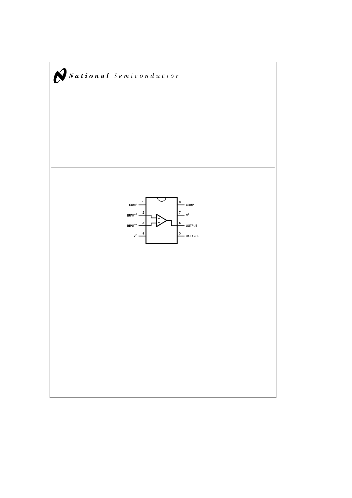
Connection Diagram
Dual-In-Line Package
TL/H/11478– 2
Top View
Order Number LM748CN
See NS Package Number N08B
C
1995 National Semiconductor Corporation RRD-B30M115/Printed in U. S. A.
Absolute Maximum Ratings
If Military/Aerospace specified devices are required,
please contact the National Semiconductor Sales
Office/Distributors for availability and specifications.
Supply Voltage
g
22V
Power Dissipation (Note 1) 500 mW
Differential Input Voltage
g
30V
Input Voltage (Note 2)
g
15V
Output Short-Circuit Duration (Note 3)
Operating Temperature Range:
LM748C 0
§
Ctoa70C
Storage Temperature Range
b
65§Ctoa150§C
Lead Temperature (Soldering, 10 sec.)
a
300§C
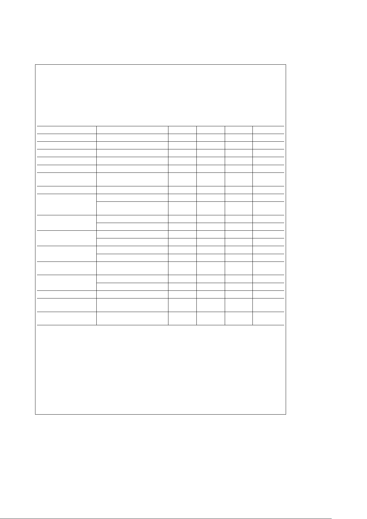
Electrical Characteristics (Note 4)
Parameter Conditions Min Typ Max Units
Input Offset Voltage T
A
e
25§C, R
S
s
10 kX 1.0 5.0 mV
Input Offset Current T
A
e
25§C 40 200 nA
Input Bias Current T
A
e
25§C 120 500 nA
Input Resistance T
A
e
25§C 300 800 kX
Supply Current T
A
e
25§C, V
S
e
g
15V 1.8 2.8 mA
Large Signal T
A
e
25§C, V
S
e
g
15V
50 160 V/mV
Voltage Gain V
OUT
e
g
10V, R
L
t
2kX
Input Offset Voltage R
S
s
10 kX 6.0 mV
Average Temperature R
S
s
50X 3.0 mV/§C
Coefficient of Input
R
S
s
10 kX
6.0 mV/
§
C
Offset Voltage
Input Offset Current T
A
e
0§Ctoa70§C 300 nA
T
A
eb
55§Ctoa125§C 500 nA
Input Bias Current T
A
e
0§Ctoa70§C 0.8 mA
T
A
eb
55§Ctoa125§C 1.5 mA
Supply Current T
A
ea
125§C, V
S
e
g
15V 1.2 2.25 mA
T
A
eb
55§Ctoa125§C 1.9 3.3 mA
Large Signal V
S
e
g
15V, V
OUT
e
g
10V
25 V/mV
Voltage Gain R
L
t
2kX
Output Voltage V
S
e
g
15V, R
L
e
10 kX
g
12
g
14 V
Swing
V
S
e
g
15V, R
L
e
2kX
g
10
g
13 V
Input Voltage Range V
S
e
g
15V
g
12 V
Common-Mode R
S
s
10 kX
70 90 dB
Rejection Ratio
Supply Voltage R
S
s
10 kX
77 90 dB
Rejection Ratio
Note 1: For operating at elevated temperatures, the device must be derated based on a maximum junction to case thermal resistance of 45§C per watt, or 150§C
per watt junction to ambient. (See Curves).
Note 2: For supply voltages less than
g
15V, the absolute maximum input voltage is equal to the supply voltage.
Note 3: Continuous short circuit is allowed for case temperatures to
a
125§C and ambient temperatures toa70§C.
Note 4: These specifications apply for
g
5VsV
S
s
a
15V and 0§CsT
A
s
a
70§C, unless otherwise specified.
2
 Loading...