

LM7372
High Speed, High Output Current, Dual Operational
Amplifier
General Description
The LM7372 is a high speed dual voltage feedback amplifier
that has the slewing characteristic of current feedback amplifiers; yet it can be used in all traditional voltage feedback
amplifier configurations.
The LM7372 is stable for gains as low as +2 or −1. It
provides a very high slew rate at 3000V/µs and a wide gain
bandwidth product of 120MHz, while consuming only
6.5mA/per amplifier ofsupplycurrent. It is ideal for video and
high speed signal processing applications such as xDSL and
pulse amplifiers. With 150mA output current, the LM7372
can be used for video distribution, as a transformer driver or
as a laser diode driver.
Operation on
±
15V power supplies allows for large signal
swings and provides greater dynamic range and
signal-to-noise ratio. The LM7372 offers high SFDR and low
THD, ideal for ADC/DAC systems. In addition, the LM7372 is
specified for
±
5V operation for portable applications.
The LM7372 is built on National’s Advance VIP
™
III (Verti-
cally integrated PNP) complementary bipolar process.
Features
n −80dBc highest harmonic distortion@1MHz, 2V
PP
n Very high slew rate: 3000V/µs
n Wide gain bandwidth product: 120MHz
n −3dB frequency
@
AV= +2: 200MHz
n Low supply current: 13mA (both amplifiers)
n High open loop gain: 85dB
n High output current: 150mA
n Differential gain and phase: 0.01%, 0.02˚
Applications
n HDSL and ADSL Drivers
n Multimedia broadcast systems
n Professional video cameras
n CATV/Fiber optics signal processing
n Pulse amplifiers and peak detectors
n HDTV amplifiers
Typical Application
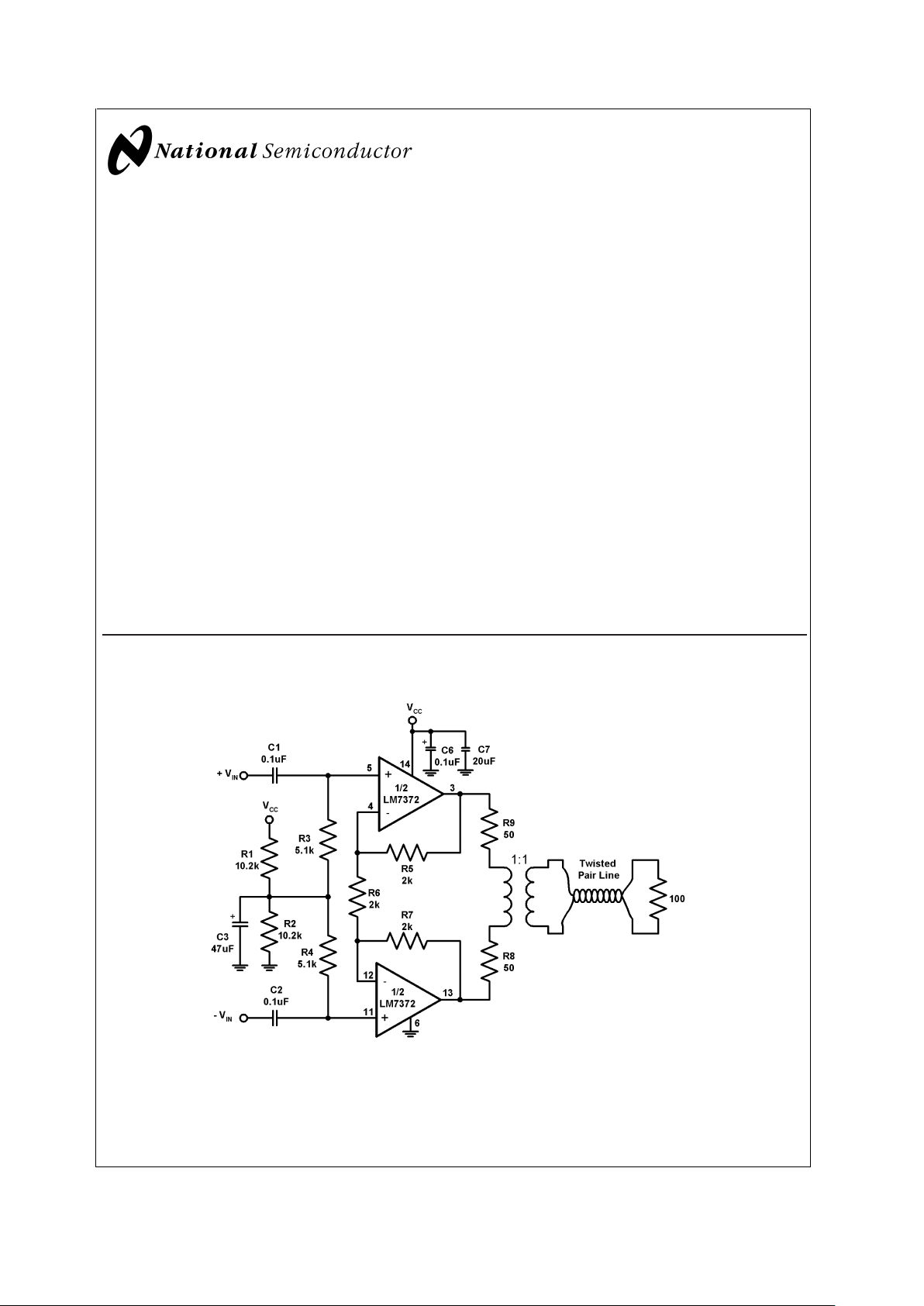
20004903
FIGURE 1. Single Supply Application (SOIC-16)
February 2002
LM7372 High Speed, High Output Current, Dual Operational Amplifier
© 2002 National Semiconductor Corporation DS200049 www.national.com
Connection Diagrams
16-Pin SOIC 8-Contact LLP
20004902
Top View
*
Heatsink Pins. See note 4
20004901
Top View
8-Pin PSOP
20004929
Top View
For PSOP SOIC-8 the exposed pad should be tied either to V−or left
electrically floating. (die attach material is conductive and is internally
tied to V
−
)
Ordering Information
Symbol Temperature Range Package Markiing Transport Media NSC
Drawing
−40˚C to +85˚C
16-Pin SOIC
LM7372IMA LM7372IMA Rails
M16A
LM7372IMAX LM7372IMA 2.5k Units Tape and Reel
8-Pin LLP
LM7372ILD L7372 1k Units Tape and Reel
LDC08A
LM7372ILDX L7372 4.5k Units Tape and Reel
8-Pin PSOP
LM7372MR LM7372MR Rails
MRA08A
LM7372MRX LM7372MR 2.5k Units Tape and Reel
LM7372
www.national.com 2
Absolute Maximum Ratings (Notes 1,
3)
If Military/Aerospace specified devices are required,
please contact the National Semiconductor Sales Office/
Distributors for availability and specifications.
ESD Tolerance
Human Body Model 1.5kV (Note 2)
Machine Model 200V (Note 2)
Suppy Voltage (V
+−V−
) 36V
Differential Input Voltage (V
S
=±15V)
±
10V
Output Short Circuit to Ground
(Note 3) Continuous
Storage Temp. Range −65˚C to 150˚C
Soldering Information
Infrared or Convection Reflow (20
sec.) 235˚C
Wave Soldering Lead Temperature
(10 sec.) 260˚C
Input Voltage V
−
to V
+
Maximum Junction Temperature
(Note 4) 150˚C
Operating Ratings (Note 1)
Supply Voltage 9V ≤ V
S
≤ 36V
Junction Temperature Range(T
J
)
LM7372 −40˚C ≤ T
J
≤ 85˚C
Thermal Resistance(θ
JA
)
16-Pin SOIC See (Note 4) 106˚C/W
70˚C/W
LLP-8 Package
(See Application Section) 40˚C/W
8-Pin PSOP
(See Application Section) 59˚C/W
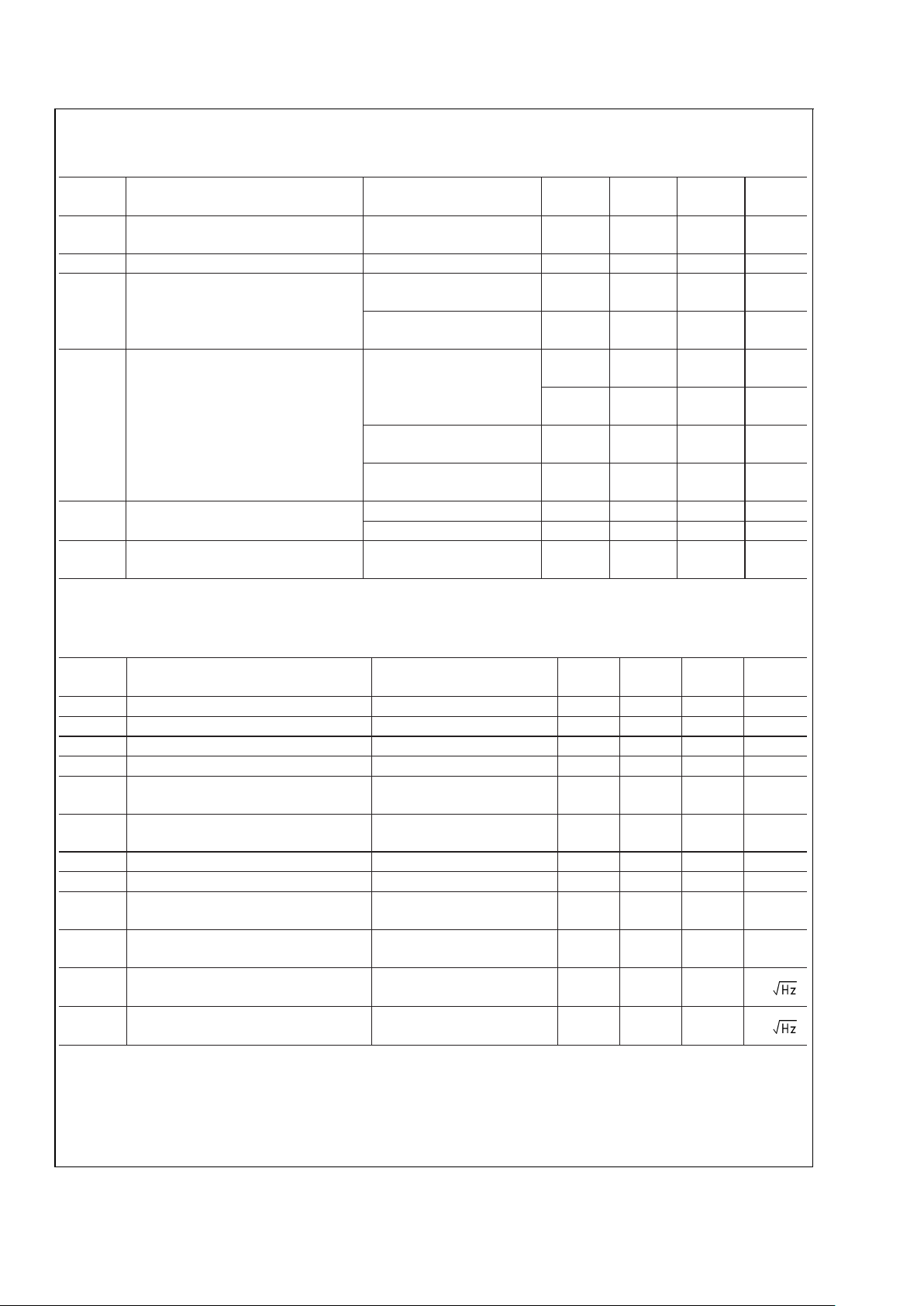
±
15V DC Electrical Characteristics
Unless otherwise specified, all limits guaranteed for TJ= 25˚C, VCM= 0V and RL=1kΩ.Boldface apply at the temperature
extremes.
Symbol Parameter Conditions Min
(Note 6)
Typ
(Note 5)
Max
(Note 6)
Units
V
OS
Input Offset Voltage 2.0 8.0
10.0
mV
TC V
OS
Input Offset Voltage Average Drift 12 µV/˚C
I
B
Input Bias Current 2.7 10
12
µA
I
OS
Input Offset Current 0.1 4.0
6.0
µA
R
IN
Input Resistance Common Mode 40 MΩ
Differential Mode 3.3 MΩ
R
O
Open Loop Output Resistance 15 Ω
CMRR Common Mode Rejection Ratio V
CM
=±10V 75
70
93 dB
PSRR Power Supply Rejection Ratio V
S
=±15V to±5V 75
70
90 dB
V
CM
Input Common-Mode Voltage Range CMRR>60dB
±
13 V
A
V
Large Signal Voltage Gain (Note 7) RL=1kΩ 75
70
85 dB
R
L
= 100Ω 70
66
81 dB
V
O
Output Swing RL=1kΩ 13
12.7
13.4 V
−13
−12.7
−13.3 V
I
OUT
= − 150mA 11.8
11.4
12.4 V
I
OUT
= 150mA −11.2
−10.8
−11.9 V
I
SC
Output Short Circuit Current Sourcing 260 mA
Sinking 250 mA
LM7372
www.national.com3
±
15V DC Electrical Characteristics (Continued)
Unless otherwise specified, all limits guaranteed for TJ= 25˚C, VCM= 0V and RL=1kΩ.Boldface apply at the temperature
extremes.
Symbol Parameter Conditions Min
(Note 6)
Typ
(Note 5)
Max
(Note 6)
Units
I
S
Supply Current (both Amps) 13 17
19
mA
±
15V AC Electrical Characteristics
Unless otherwise specified, all limits guaranteed for TJ= 25˚C, VCM= 0V and RL=1kΩ.Boldface apply at the temperature
extremes.
Symbol Parameter Conditions Min
(Note 6)
Typ
(Note 5)
Max
(Note 6)
Units
SR Slew Rate (Note 8) A
V
= +2, VIN13V
P-P
3000 V/µs
A
V
= +2, VIN10V
P-P
2000
Unity Bandwidth Product 120 MHz
−3dB Frequency A
V
= +2 220 MHz
φ
m
Phase Margin A
VOL
= 6dB 70 deg
t
S
Settling Time (0.1%) AV= −1, AO=±5V,
R
L
= 500Ω
50 ns
t
P
Propagation Delay AV= −2, VIN=±5V,
R
L
= 500Ω
6.0 ns
A
D
Differential Gain (Note 9) 0.01 %
φ
D
Differential Phase (Note 9) 0.02 deg
hd2 Second Harmonic Distortion
F
IN
= 1MHz, AV=+2
V
OUT
=2V
P-P,RL
= 100Ω −80 dBc
V
OUT
= 16.8V
P-P,RL
= 100Ω −73 dBc
hd3 Third Harmonic Distortion
F
IN
= 1MHz, AV=+2
V
OUT
=2V
P-P,RL
= 100Ω −91 dBc
V
OUT
= 16.8V
P-P,RL
= 100Ω −67 dBc
IMD Intermodulation Distortion Fin 1 = 75kHz,
Fin 2 = 85kHz
V
OUT
= 16.8V
P-P,RL
= 100Ω
−87 dBc
e
n
Input-Referred Voltage Noise f = 10kHz 14 nV/
i
n
Input-Referred Current Noise f = 10kHz 1.5 pA/
±
5V DC Electrical Characteristics
Unless otherwise specified, all limits guaranteed for TJ= 25˚C, VCM= 0V and RL=1kΩ.Boldface apply at the temperature
extremes.
Symbol Parameter Conditions Min
(Note 6)
Typ
(Note 5)
Max
(Note 6)
Units
V
OS
Input Offset Voltage 2.2 8.0
10.0
mV
TC V
OS
Input Offset Voltage Average Drift 12 µV/˚C
I
B
Input Bias Current 3.3 10
12
µA
I
OS
Input Offset Current 0.1 4
6
µA
R
IN
Input Resistance Common Mode 40 MΩ
Differential Mode 3.3 MΩ
R
O
Open Loop Output Resistance 15 Ω
CMRR Common Mode Rejection Ratio V
CM
=±2.5V 70
65
90 dB
LM7372
www.national.com 4
±
5V DC Electrical Characteristics (Continued)
Unless otherwise specified, all limits guaranteed for TJ= 25˚C, VCM= 0V and RL=1kΩ.Boldface apply at the temperature
extremes.
Symbol Parameter Conditions Min
(Note 6)
Typ
(Note 5)
Max
(Note 6)
Units
PSRR Power Supply Rejection Ratio V
S
=±15V to±5V 75
70
90 dB
V
CM
Input Common-Mode Voltage Range CMRR>60dB
±
3V
A
V
Large Signal Voltage Gain (Note 7) RL=1kΩ 70
65
78 dB
R
L
= 100Ω 64
60
72 dB
V
O
Output Swing RL=1kΩ 3.2
3.0
3.4 V
−3.2
−3.0
−3.4 V
I
OUT
= − 80mA 2.5
2.2
2.8 V
I
OUT
= 80mA −2.5
−2.2
−2.7 V
I
SC
Output Short Circuit Current Sourcing 150 mA
Sinking 150 mA
I
S
Supply Current (both Amps) 12.4 16
18
mA
±
5V AC Electrical Characteristics
Unless otherwise specified, all limits guaranteed for TJ= 25˚C, VCM= 0V and RL=1kΩ.Boldface apply at the temperature
extremes.
Symbol Parameter Conditions Min
(Note 6)
Typ
(Note 5)
Max
(Note 6)
Units
SR Slew Rate (Note 8) A
V
= +2, VIN3V
P-P
700 V/µs
Unity Bandwidth Product 100 MHz
−3dB Frequency A
V
= +2 125 MHz
φ
m
Phase Margin 70 deg
t
S
Settling Time (0.1%) AV= −1, VO=±1V, RL=
500Ω
70 ns
t
P
Propagation Delay AV= +2, VIN=±1V, RL=
500Ω
7ns
A
D
Differential Gain (Note 9) 0.02 %
φ
D
Differential Phase (Note 9) 0.03 deg
hd2 Second Harmonic Distortion
F
IN
= 1MHz, AV=+2
V
OUT
=2V
P-P,RL
= 100Ω −84 dBc
hd3 Third Harmonic Distortion
F
IN
= 1MHz, AV=+2
V
OUT
=2V
P-P,RL
= 100Ω −94 dBc
e
n
Input-Referred Voltage Noise f = 10kHz 14 nV/
i
n
Input-Referred Current Noise f = 10kHz 1.8 pA/
Note 1: Absolute Maximum Ratings indicate limits beyond which damage to the device may occur. Operating Ratings indicate conditions for which the device is
intended to be functional, but specific performance is not guaranteed. For guaranteed specifications and the test conditions, see the Electrical Characteristics.
Note 2: For testing purposes, ESD was applied using human body model, 1.5kΩ in series with 100pF. Machine model, 0Ω in series with 200pF.
Note 3: Applies to both single-supply and split-supply operation. Continuous short circuit operation at elevated ambient temperature can result in exceeding the
maximum allowed junction temperature of 150˚C.
LM7372
www.national.com5

±
5V AC Electrical Characteristics (Continued)
Note 4: The maximum power dissipation is a function of T
(JMAX)
, θJA, and TA. The maximum allowable power dissipation at any ambient temperature is PD=
(T
(JMAX)–TA
)/θJA. All numbers apply for packages soldered directly into a PC board. The value for θJAis 106˚C/W for the SOIC 16 package. With a total area of
4sq. in of 1oz CU connected to pins 1,6,8,9 & 16, θ
JA
for the SOIC 16 is decreased to 70˚C/W.
Note 5: Typical values represent the most likely parametic norm.
Note 6: All limits are guaranteed by testing or statistical analysis.
Note 7: Largesignal voltage gain is the total output swing divided by the input signal required to produce that swing. For V
S
=±15V,V
OUT
=±10V.For VS=±5V,
V
OUT
=±2V
Note 8: Slew Rate is the average of the rising and falling slew rates.
Note 9: Differential gain and phase are measured with A
V
= +2, VIN=1VPPat 3.58 MHz and output is 150Ω terminated.
Typical Performance Characteristics
Harmonic Distortion vs. Frequency
20004904
Harmonic Distortion vs. Frequency
20004905
Harmonic Distortion vs. Frequency
20004906
Harmonic Distortion vs. Frequency
20004907
LM7372
www.national.com 6

Typical Performance Characteristics (Continued)
Harmonic Distortion vs. Output Level Harmonic Distortion vs. Output Level
20004908 20004909
Harmonic Distortion vs. Output Level Harmonic Distortion vs. Output Level
20004910 20004911
Harmonic Distortion vs. Load Resistance Harmonic Distortion vs. Load Resistance
20004912 20004913
LM7372
www.national.com7

Typical Performance Characteristics (Continued)
Harmonic Distortion vs. Load Resistance Harmonic Distortion vs. Load Resistance
20004914 20004915
Frequency Response Frequency Response
20004916
20004917
Frequency Response Small Signal Pulse Response
20004918
20004920
LM7372
www.national.com 8

Typical Performance Characteristics (Continued)
Large Signal Pulse Response Thermal Performance of 8ld-LLP
20004921
20004922
Harmonic Distortion vs. Frequency Input Bias Current (µA) vs. Temperature
20004927
20004923
Output Voltage vs. Output Current
20004924
LM7372
www.national.com9

Simplified Schematic Diagram
20004928
Application Notes
The LM7372 is a high speed dual operational amplifier with
a very high slew rate and very low distortion, yet like many
other op amps, it is used in conventional voltage feedback
amplifier applications. Also, again like many op amps, it has
a class AB output stage in order to be able to deliver high
currents to low impedance loads, yet draw very little quiescent supply current. For most op-amps in typical applications, this topology means that internal power dissipation is
rarely an issue, even with the trend to smaller surface mount
packages. However, the LM7372 has been designed for
applications where significant levels of power dissipation will
be encountered, and an effective means of removing the
internal heat generated by this power dissipation is needed
to maintain the semiconductor junction temperature at acceptable levels, particularly in environments with elevated
ambient temperatures.
Several factors contribute to power dissipation and consequently higher semiconductor junction temperatures, and
these factors need to be well understood if the LM7372 is to
perform to the desired specifications in a given application.
Since different applications will have different dissipation
levels and different compromises can be made between the
ways these factors will contribute to the total junction temperature, this section will examine the typical application
shown on the front page of this data sheet as an example,
and offer suggestions for solutions where excessive junction
temperatures are encountered.
There are two major contributors to the internal power dissipation; the product of the supply voltage and the LM7372
quiescent current when no signal is being delivered to the
external load, and the additional power dissipated while
delivering power to the external load. The first of these
components is easy to calculate simply by inspection of the
data sheet. The LM7372 quiescent supply current is given as
6.5mA per amplifier, so with a 24Volt supply the power
dissipation is
PQ=V
S
x 2Iq (VS=VCC+VEE)
= 24 x (6.5 x 10-3)
= 312mW
This is already a high level of internal power dissipation, and
in a small surface mount package with a thermal resistance
(θ
JA
= 140˚C/Watt (a not unreasonable value for an SO-8
package) would result in a junction temperature 140˚C/W x
0.312W = 43.7˚C above the ambient temperature. A similar
calculation using the worst case maximum current limit at an
85˚C ambient will yield a power dissipation of 456mW with a
junction temperature of 149˚C, perilously close to the maximum permitted junction temperature of 150˚C!
The second contributor to high junction temperature is the
additional power dissipated internally when power is being
delivered to the external load. This cause of temperature rise
can be less amenable to calculation, even when the actual
operating conditions are known.
For a Class B output stage, one transistor of the output pair
will conduct the load current as the output voltage swings
positive, with the other transistor drawing no current, and
hence dissipating no power. During the other half of the
signal swing this situation is reversed, with the lower transistor sinking the load current and the upper transistor is cut off.
The current in each transistor will be a half wave rectified
version of the total load current. Ideally neither transistor will
dissipate power when there is no signal swing, but will
dissipate increasing power as the output current increases.
However, as the signal voltage across the load increases
with load current, the voltage across the output transistor
(which is the difference voltage between the supply voltage
and the instantaneous voltage across the load) will decrease
and a point will be reached where the dissipation in the
transistor will begin to decrease again. If the signal is driven
into a square wave, ideally the transistor dissipation will fall
all the way back to zero.
LM7372
www.national.com 10

Application Notes (Continued)
For each amplifier then, with an effective load each of R
L
and
a sine wave source, integration over the half cycle with a
supply voltage V
S
and a load voltage VLyields the average
power dissipation
P
D=VSVL
/πRL-V
L
2
/2RL..........(1)
Where V
S
is the supply voltage and VLis the peak signal
swing across the load R
L
.
For the package, the power dissipation will be doubled since
there are two amplifiers in the package, each contributing
half the swing across the load.
The circuit in
Figure 1
is using the LM7372 as the upstream
driver in an ADSL application with Discrete MultiTone modulation. With DMT the upstream signal is spread into 32
adjacent channels each 4kHz wide. For transmission over
POTS, the regular telephone service, this upstream signal
from the CPE (Customer Premise Equipment) occupies a
frequency band from around 20kHz up to a maximum frequency of 135kHz. At first sight, these relatively low transmission frequencies certainly do not seem to require the use
of very high speed amplifiers with GBW products in the
range of hundreds of megahertz. However, the close spacing of multiple channels places stringent requirements on the
linearity of the amplifier, since non-linearities in the presence
of multiple tones will cause harmonic products to be generated that can easily interfere with the higher frequency down
stream signals also present on the line. The need to deliver
3rd Harmonic distortion terms lower than −75dBc is the
reason for the LM7372 quiescent current levels. Each amplifier is running over 3mA in the output stage alone in order
to minimize crossover distortion.
xDSL signal levels are adjusted to provide a given power
level on the line, and in the case of ADSL this is an average
power of 13dBm. For a line with a characteristic impedance
of 100Ω this is only 20mW. Because the transformer shown
in
Figure 1
is part of a transceiver circuit, two
back-termination resistors are connected in series with each
amplifier output. Therefore the equivalent R
L
for each amplifier is also 100Ω, and each amplifier is required to deliver
20mW to this load.
Since V
L
2
/2RL = 20mW then VL= 2V(peak).
Using Equation (1) with this value for signal swing and a 24V
supply, the internal power dissipation per amplifier is
132.8mW. Adding the quiescent power dissipation to the
amplifier dissipation gives the total package internal power
dissipation as
P
D(Total)
= 312mW + (2 x 132.8mW) = 578mW
This result is actually quite pessimistic because it assumes
that the dissipation as a result of load current is simply added
to the dissipation as a result of quiescent current. This is not
correct since the AB bias current in the output stage is
diverted to load current as the signal swing amplitude increases from zero. In fact with load currents in excess of
3.3mA, all the bias current is flowing in the load, consequently reducing the quiescent component of power dissipation.Also, it assumes a sine wave signal waveform when the
actual waveform is composed of many tones of different
phases and amplitudes which may demonstrate lower average power dissipation levels.
The average current for a load power of 20mW is 14.1mA.
Neglecting the AB bias current this appears as a full-wave
rectified current waveform in the supply current with a peak
value of 19.9mA. The peak to average ratio for a waveform
of this shape is 1.57, so the total average load current is
12.7mA. Adding this to the quiescent current, and subtracting the power dissipated in the load gives the same package
power dissipation level calculated above. Nevertheless,
when the supply current peak swing is measured, it is found
to be significantly lower because the AB bias current is
contributing to the load current. The supply current has a
peak swing of only 14mA (compared to 19.9mA) superimposed on the quiescent current, with a total average value of
only 21mA. Therefore the total package power dissipation in
this application is
P
D(Total)
=(VSx Iavg) - Power in Load
= (24 x 21)mW - 40mW
= 464mW
This level of power dissipation would not take the junction
temperature in the SO-8 package over the absolute maximum rating at elevated ambient temperatures (barely), but
there is no margin to allow for component tolerances or
signal variances.
To develop 20mW in a 100Ω requires each amplifier to
deliver a peak voltage of only 2V, or 4V(
P-P
). This level of
signal swing does not require a high supply voltage but the
application uses a 24V supply. This is because the modulation technique uses a large number of tones to transmit the
data. While the average power level is held to 20mW,at any
time the phase and amplitude of individual tones will be such
as to generate a combined signal with a higher peak value
than 2V. For DMT this crest factor is taken to be around 5.33
so each amplifier has to be able to handle a peak voltage
swing of
V
Lpeak
= 1.4 x 5.33 = 7.5V or 15V(
P-P
)
If other factors, such as transformer loss or even higher peak
to average ratios are allowed for, this means the amplifiers
must each swing between 16 to 18V(
P-P
).
The required signal swing can be reduced by using a step-up
transformer to drive the line. For example a 1:2 ratio will
reduce the peak swing requirement by half, and this would
allow the supply to be reduced by a corresponding amount.
This is not recommended for the LM7372 in this particular
application for two reasons. Although the quiescent power
contribution to the overall dissipation is reduced by about
150mW, the internal power dissipation to drive the load
remains the same, since the load for each amplifier is now
25Ω instead of 100Ω. Furthermore, this is a transceiver
application where downstream signals are simultaneously
appearing at the transformer secondary. The down stream
signals appear differentially across the back termination resistors and are now stepped down by the transformer turns
ratio with a consequent loss in receiver sensitivity compared
to using a 1:1 transformer.Any trade-off to reduce the supply
voltage by an increase in turns ratio should bear these
factors in mind, as well as the increased signal current levels
required with lower impedance loads.
At an elevated ambient temperature of 85˚C and with an
average power dissipation of 464mW, a package thermal
resistance between 60˚C/W and 80˚C/W will be needed to
keep the maximum junction temperature in the range 110˚C
to 120˚C. The PSOP or LLP package would be the package
of choice here with ample board copper area to aid in heat
dissipation (see table 2).
For most standard surface mount packages, SO-8, SO-14,
SO-16 etc, the only means of heat removal from the die is
through the bond wires to external copper connecting to the
leads. Usually it will be difficult to reduce the thermal resis-
LM7372
www.national.com11

Application Notes (Continued)
tance of these packages below 100˚C/W by these methods
and several manufacturers, including National, offer package modifications to enhance the thermal characteristics.
Improved removal of internal heat can be achieved by directly connecting bond wires to the lead frame inside the
package. Since this lead frame supports the die attach
paddle, heat is transferred directly from the substrate to the
outside copper by these bond wires. For an 8 pin package,
this enhancement is somewhat limited since only the V-bond
wire can be used, because it is the only lead at the same
voltage as the substrate and there is an electrical connection
as well as a thermal connection.
The LM7372 is available in the SOIC-16 package. Since only
8 pins are needed for the two operational amplifiers, the
remaining pins are used for heat sink purposes. Each of the
end pins, 1,8,9 & 16 are internally bonded to the lead frame
and form an effective means of transferring heat to external
copper. This external copper can be either electrically isolated or be part of the topside ground plane in a single supply
application.
Figure 2
. shows a copper pattern which can be used to
dissipate internal heat from the LM7372.
Table 1
gives some
values of θ
JA
for different values of L and H with 1oz copper.
TABLE 1. Thermal Resistance with Area of Cu
Package L (in) H (in) θJA(˚C/W)
SOIC 16 1 0.5 83
SOIC 16 2 1 70
SOIC 16 3 1.5 67
From
Table 1
it is apparent that two areas of 1oz copper at
each end of the package, each 2 in
2
in area (for a total of
2600mm
2
) will be sufficient to hold the maximum junction
temperature under 120˚C with an 85˚C ambient temperature.
An even better package for removing internally generated
heat is a package with an exposed die attach paddle. The
LM7372 is also available in the 8 lead LLP and PSOP
packages. For these packages the entire lower surface of
the paddle is not covered with plastic, which would otherwise
act as a thermal barrier to heat transfer. Heat is transferred
directly from the die through the paddle rather than through
the small diameter bonding wires. Values of θ
JA
in ˚C/W for
the LLP package with various areas and weights of copper
are tabulated below.
TABLE 2. Thermal Resistance of LLP Package
Copper Area 0.5 in
2
1.0 in
2
2.0 in
2
Top
Layer
Only
0.5 oz
1.0 oz
2.0 oz
115
91
74
105
79
60
102
72
52
Bottom
Layer
Only
0.5 oz
1.0 oz
2.0 oz
102
92
85
88
75
66
81
65
54
Top And
Bottom
0.5 oz
1.0 oz
2.0 oz
83
71
63
70
57
48
63
47
37
Table 2
clearly demonstrates the superior thermal qualities
of the exposed pad package. For example, using the topside
copper only in the same way as shown for the SOIC package
(
Figure 2
), with the L dimension held at 1 inch, the LLP
requires half the area of 1 oz copper at each end of the
package (1 in
2
, for a total of 1300mm2), for a comparable
thermal resistance of 72˚C/Watt. This gives considerably
more flexibility in the pcb layout aside from using less copper.
The shape of the heat sink shown in
Figure 2
is necessary to
allow external components to be connected to the package
pins. If thermal vias are used beneath the LLP to the bottom
side ground plane, then a square pattern heat sink can be
used and there is no restriction on component placement on
the top side of the board. Even better thermal characteristics
are obtained with bottom layer heatsinking. A 2 inch square
of 0.5oz copper gives the same thermal resistance (81˚C/W)
as a competitive thermally enhanced SO-8 package which
needs two layers of 2 oz copper, each 4 in
2
(for a total of
5000 mm
2
). With heavier copper, thermal resistances as low
as 54˚C/W are possible with bottom side heatsinking only,
substantially improving the long term reliability since the
maximum junction temperature is held to less than 110˚C,
even with an ambient temperature of 85˚C. If both top and
bottom copper planes are used, the thermal resistance can
be brought to under 40˚C/W.
Power Supplies
The LM7372 is fabricated on a high voltage, high speed
process. Using high supply voltages ensures adequate
headroom to give low distortion with large signal swings. In
Figure 1
, a single 24V supply is used. To maximize the
output dynamic range the non-inverting inputs are biassed to
half supply voltage by the resistive divider R1, R2. The input
signals are AC coupled and the coupling capacitors (C1, C2)
can be scaled with the bias resistors (R3, R4) to form a high
pass filter if unwanted coupling from the POTS signal occurs.
Supply decoupling is important at both low and high frequencies. The 10µF Tantalum and 0.1µF Ceramic capacitors
should be connected close to the supply Pin 14. Note that
the V
−
pin (pin 6), and the PCB area associated with the
heatsink (Pins 1,8,9 & 16) are at the same potential. Any
layout should avoid running input signal leads close to this
ground plane, or unwanted coupling of high frequency supply currents may generate distortion products.
Although this application shows a single supply, conversion
to a split supply is straightforward. The half supply resistive
20004925
FIGURE 2. Copper Heatsink Patterns
LM7372
www.national.com 12

Application Notes (Continued)
divider network is eliminated and the bias resistors at the
non-inverting inputs are returned to ground, see
Figure 3
(the pin numbers in
Figure 3
are given for the LLP and PSOP
packages, those in
Figure 1
are for the SOIC package). With
a split supply, note that the ground plane and the heatsink
copper must be separate and are at different potentials, with
the heatsink (pin 4 of the LLPand PSOP, pins 6,1,8,9 &16 of
the SOIC) now at a negative potential (V
−
).
In either configuration, the area under the input pins should
be kept clear of copper (Whether ground plane copper or
heatsink copper) to avoid parasitic coupling to the inputs.
The LM7372 is stable with non inverting closed loop gains as
low as +2. Typical of any voltage feedback operational amplifier, as the closed loop gain of the LM7372 is increased,
there is a corresponding reduction in the closed loop signal
bandwidth. For low distortion performance it is recommended to keep the closed loop bandwidth at least 10X the
highest signal frequency. This is because there is less loop
gain (the difference between the open loop gain and the
closed loop gain) available at higher frequencies to reduce
harmonic distortion terms.
Printed Circuit Board Layout and Evaluation Boards:
Generally, a good high-frequency layout will keep power
supply and ground traces away from the inverting input and
output pins. Parasitic capacitance on these nodes to ground
will cause frequency response peaking and possible circuit
oscillations (see Application Note OA-15 for more information). National Semiconductor suggests the following evaluation boards as a guide for high frequency layout and as an
aid in device testing and characterization:
Device Package Evaluation
Board PN
LM7372MA 16-Pin SOIC None
LM7372ILD 8-Pin LLP CLC730114
LM7372MR 8-Pin PSOP CLC730121
These free evaluation boards are shipped automatically
when a device sample request is placed with National Semiconductor.
The DAP (die attach paddle) on the LLP-8, and the PSOP
should be tied to V
−
. It should not be tied to ground. See
respective Evaluation Board documentation.
20004926
FIGURE 3. Split Supply Application (LLP)
LM7372
www.national.com13

Physical Dimensions inches (millimeters)
unless otherwise noted
16-Pin SOIC
NS Package Number M16A
8-Pin LLP
NS Package Number LDC08A
LM7372
www.national.com 14

Physical Dimensions inches (millimeters) unless otherwise noted (Continued)
8-Pin PSOP
NS Package Number MRA08A
LIFE SUPPORT POLICY
NATIONAL’S PRODUCTS ARE NOT AUTHORIZED FOR USE AS CRITICAL COMPONENTS IN LIFE SUPPORT
DEVICES OR SYSTEMS WITHOUT THE EXPRESS WRITTEN APPROVAL OF THE PRESIDENT AND GENERAL
COUNSEL OF NATIONAL SEMICONDUCTOR CORPORATION. As used herein:
1. Life support devices or systems are devices or
systems which, (a) are intended for surgical implant
into the body, or (b) support or sustain life, and
whose failure to perform when properly used in
accordance with instructions for use provided in the
labeling, can be reasonably expected to result in a
significant injury to the user.
2. A critical component is any component of a life
support device or system whose failure to perform
can be reasonably expected to cause the failure of
the life support device or system, or to affect its
safety or effectiveness.
National Semiconductor
Corporation
Americas
Email: support@nsc.com
National Semiconductor
Europe
Fax: +49 (0) 180-530 85 86
Email: europe.support@nsc.com
Deutsch Tel: +49 (0) 69 9508 6208
English Tel: +44 (0) 870 24 0 2171
Français Tel: +33 (0) 1 41 91 8790
National Semiconductor
Asia Pacific Customer
Response Group
Tel: 65-2544466
Fax: 65-2504466
Email: ap.support@nsc.com
National Semiconductor
Japan Ltd.
Tel: 81-3-5639-7560
Fax: 81-3-5639-7507
www.national.com
LM7372 High Speed, High Output Current, Dual Operational Amplifier
National does not assume any responsibility for use of any circuitry described, no circuit patent licenses are implied and National reserves the right at any time without notice to change said circuitry and specifications.
 Loading...