LM7301
Low Power, 4 MHz GBW, Rail-to-Rail Input-Output
Operational Amplifier in TinyPak
™
Package
General Description
The LM7301 provides high performance in a wide range of
applications. The LM7301 offers greater than rail-to-rail input
range, full rail-to-rail output swing, large capacitive load driving ability and low distortion.
With only 0.6 mA supply current, the 4 MHz gain-bandwidth
of this device supports new portable applications where
higher power devices unacceptably drain battery life.
The LM7301 can be driven by voltages that exceed both
power supply rails, thus eliminating concerns over exceeding
the common-mode voltage range. The rail-to-rail output
swing capability provides the maximum possible dynamic
range at the output. This is particularly important when operating on low supply voltages.
Operating on supplies of 1.8V–32V,the LM7301 is excellent
for a very wide range of applications in low power systems.
Placing the amplifier right at the signal source reduces board
size and simplifies signal routing. The LM7301 fits easily on
low profile PCMCIA cards.
Features
at V
S
=
5V (Typ unless otherwise noted)
n Tiny SOT23-5 package saves space
n Greater than Rail-to-Rail Input CMVR −0.25V to 5.25V
n Rail-to-Rail Output Swing 0.07V to 4.93V
n Wide Gain-Bandwidth 4 MHz
n Low Supply Current 0.60 mA
n Wide Supply Range 1.8V to 32V
n High PSRR 104 dB
n High CMRR 93 dB
n Excellent Gain 97 dB
Applications
n Portable instrumentation
n Signal conditioning amplifiers/ADC buffers
n Active filters
n Modems
n PCMCIA cards
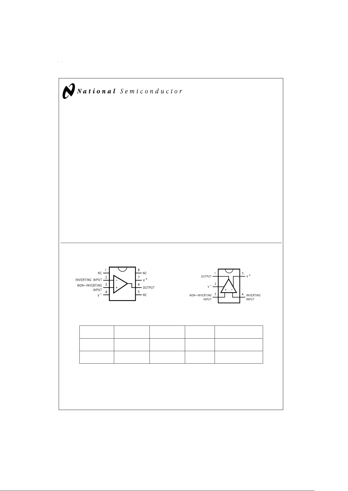
Connection Diagrams
Ordering Information
Package Ordering NSC Drawing Package Supplied As
Information Number Marking
8-Pin SO-8 LM7301IMX M08A LM7301IM 2.5k Tape and Reel
LM7301IM M08A LM7301IM Rails
5-Pin SOT23 LM7301IM5 MA05A A04A 1k Tape and Reel
LM7301IM5X MA05A A04A 3k Tape and Reel
TinyPak™is a trademark of NationalSemiconductor Corporation.
8-Pin SO-8
DS012842-1
Top View
5-Pin SOT23
DS012842-2
Top View
August 1999
LM7301 Low Power, 4 MHz GBW, Rail-to-Rail Input-Output Operational Amplifier in TinyPak
Package
© 1999 National Semiconductor Corporation DS012842 www.national.com

Absolute Maximum Ratings (Note 1)
If Military/Aerospace specified devices are required,
please contact the National Semiconductor Sales Office/
Distributors for availability and specifications.
ESD Tolerance (Note 2) 2500V
Differential Input Voltage 15V
Voltage at Input/Output Pin (V
+
) + 0.3V, (V−) −0.3V
Supply Voltage (V
+−V−
) 35V
Current at Input Pin
±
10 mA
Current at Output Pin (Note 3)
±
20 mA
Current at Power Supply Pin 25 mA
Lead Temperature
(Soldering, 10 sec.) 260˚C
Storage Temperature Range −65˚C to +150˚C
Junction Temperature (Note 4) 150˚C
Operating Ratings (Note 1)
Supply Voltage 1.8V ≤ V
S
≤ 32V
Junction Temperature Range −40˚C ≤ T
J
≤ +85˚C
Thermal Resistance (θ
JA
)
M5 Package, 5-Pin SOT23 325˚C/W
M Package,
8-Pin Surface Mount 165˚C/W
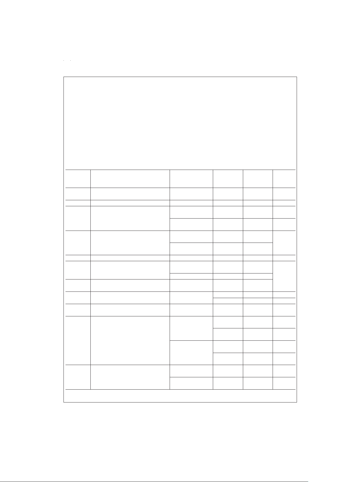
5.0V DC Electrical Characteristics
Unless otherwise specified, all limits guaranteed for T
J
=
25˚C, V
+
=
5.0V, V
−
=
0V, V
CM
=
V
O
=
V
+
/2 and R
L
>
1MΩto
V
+
/2. Boldface limits apply at the temperature extremes
Typ LM7301
Symbol Parameter Conditions (Note 5) Limit Units
(Note 6)
V
OS
Input Offset Voltage 0.03 6 mV
8 max
TCV
OS
Input Offset Voltage Average Drift 2 µV/˚C
I
B
Input Bias Current V
CM
=
0V 90 200 nA
250 max
V
CM
=
5V −40 −75 nA
−85 min
I
OS
Input Offset Current V
CM
=
0V 0.7 70 nA
max
80
V
CM
=
5V 0.7 55
65
R
IN
Input Resistance, CM 0V ≤ VCM≤ 5V 39 MΩ
CMRR Common Mode Rejection Ratio 0V ≤ V
CM
≤ 5V 88 70 dB
min
67
0V ≤ V
CM
≤ 3.5V 93
PSRR Power Supply Rejection Ratio 2.2V ≤ V
+
≤ 30V 104 87
84
V
CM
Input Common-Mode Voltage Range CMRR ≥ 65 dB 5.1 V
−0.1 V
A
V
Large Signal Voltage Gain R
L
=
10 kΩ 71 14 V/mV
V
O
=
4.0V
PP
10 min
V
O
Output Swing R
L
=
10 kΩ 0.07 0.12 V
0.15 max
4.93 4.88 V
4.85 min
R
L
=
2kΩ 0.14 0.20 V
0.22 max
4.87 4.80 V
4.78 min
I
SC
Output Short Circuit Current Sourcing 11.0 8.0 mA
5.5 min
Sinking 9.5 6.0 mA
5.0 min
www.national.com 2

5.0V DC Electrical Characteristics (Continued)
Unless otherwise specified, all limits guaranteed for T
J
=
25˚C, V
+
=
5.0V, V
−
=
0V, V
CM
=
V
O
=
V
+
/2 and R
L
>
1MΩto
V+/2. Boldface limits apply at the temperature extremes
Typ LM7301
Symbol Parameter Conditions (Note 5) Limit Units
(Note 6)
I
S
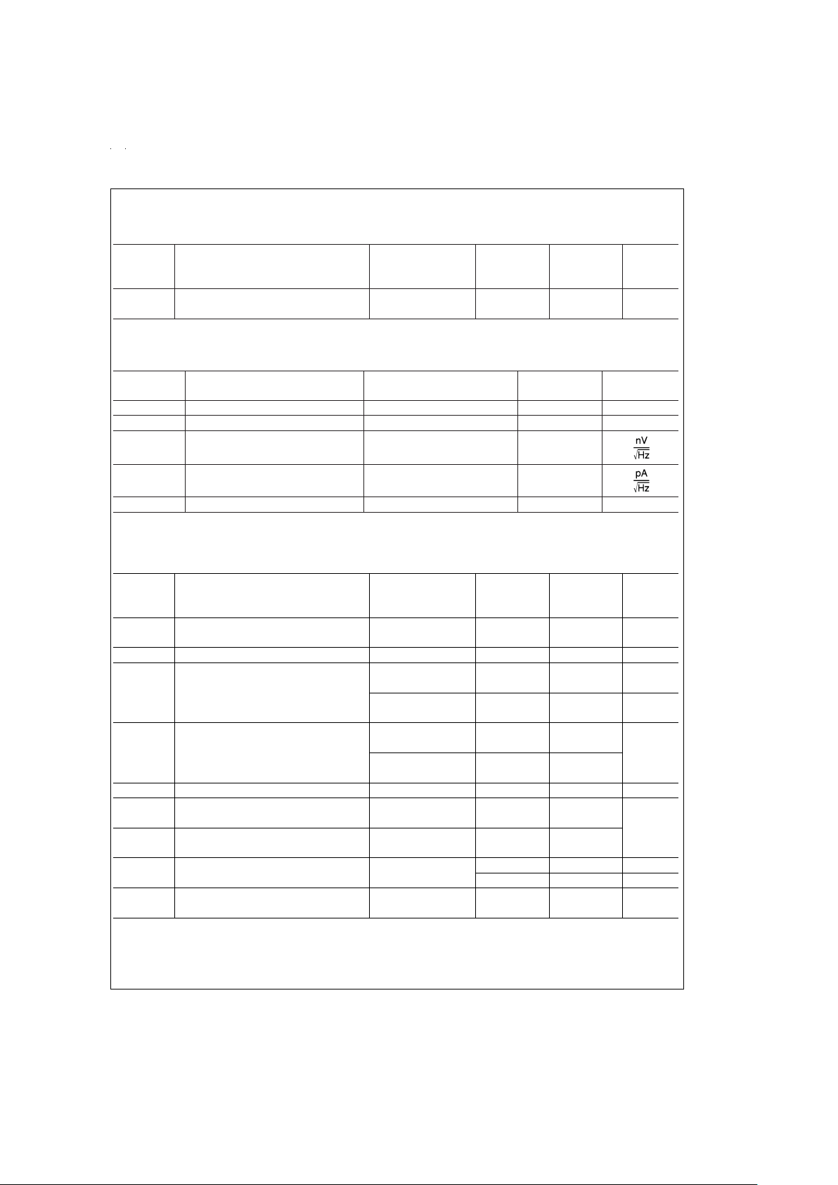
Supply Current 0.60 1.10 mA
1.24 max
AC Electrical Characteristics
T
J
=
25˚C, V
+
=
2.2V to 30V, V
−
=
0V, V
CM
=
V
O
=
V
+
/2 and R
L
>
1MΩto V+/2
Symbol Parameter Conditions Typ Units
(Note 5)
SR Slew Rate
±
4V Step@V
S
±
6V 1.25 V/µs
GBW Gain-Bandwidth Product f=100 kHz, R
L
=
10 kΩ 4 MHz
e
n
Input-Referred Voltage Noise f=1 kHz 36
i
n
Input-Referred Current Noise f=1 kHz 0.24
T.H.D. Total Harmonic Distortion f=10 kHz 0.006
%
2.2V DC Electrical Characteristics
Unless otherwise specified, all limits guaranteed for T
J
=
25˚C, V
+
=
2.2V, V
−
=
0V, V
CM
=
V
O
=
V
+
/2 and R
L
>
1MΩto
V
+
/2. Boldface limits apply at the temperature extremes
Typ LM7301
Symbol Parameter Conditions (Note 5) Limit Units
(Note 6)
V
OS
Input Offset Voltage 0.04 6 mV
8 max
TCV
OS
Input Offset Voltage Average Drift 2 µV/˚C
I
B
Input Bias Current V
CM
=
0V 89 200 nA
250 max
V
CM
=
2.2V −35 −75 nA
−85 min
I
OS
Input Offset Current V
CM
=
0V 0.8 70 nA
max
80
V
CM
=
2.2V 0.4 55
65
R
IN
Input Resistance 0V ≤ VCM≤ 2.2V 18 MΩ
CMRR Common Mode Rejection Ratio 0V ≤ V
CM
≤ 2.2V 82 60 dB
min
56
PSRR Power Supply Rejection Ratio 2.2V ≤ V
+
≤ 30V 104 87
84
V
CM
Input Common-Mode Voltage Range CMRR>60 dB 2.3 V
−0.1 V
A
V
Large Signal Voltage Gain R
L
=
10 kΩ 46 6.5 V/mV
V
O
=
1.6V
PP
5.4 min
www.national.com3

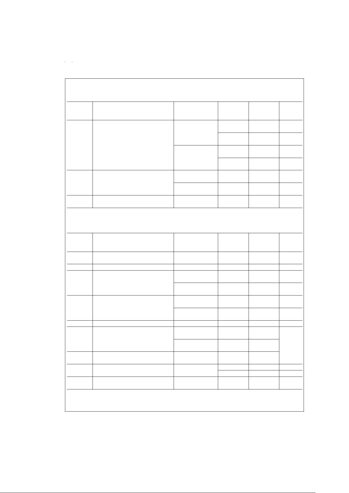
2.2V DC Electrical Characteristics (Continued)
Unless otherwise specified, all limits guaranteed for T
J
=
25˚C, V
+
=
2.2V, V
−
=
0V, V
CM
=
V
O
=
V
+
/2 and R
L
>
1MΩto
V+/2. Boldface limits apply at the temperature extremes
Typ LM7301
Symbol Parameter Conditions (Note 5) Limit Units
(Note 6)
V
O
Output Swing R
L
=
10 kΩ 0.05 0.08 V
0.10 max
2.15 2.10 V
2.00 min
R
L
=
2kΩ 0.09 0.13 V
0.14 max
2.10 2.07 V
2.00 min
I
SC
Output Short Circuit Current Sourcing 10.9 8.0 mA
5.5 min
Sinking 7.7 6.0 mA
5.0 min
I
S
Supply Current 0.57 0.97 mA
1.24 max
30V DC Electrical Characteristics
Unless otherwise specified, all limits guaranteed for T
J
=
25˚C, V
+
=
30V, V
−
=
0V, V
CM
=
V
O
=
V
+
/2 and R
L
>
1MΩto V+/2.
Boldface limits apply at the temperature extremes
Typ LM7301
Symbol Parameter Conditions (Note 5) Limit Units
(Note 6)
V
OS
Input Offset Voltage 0.04 6 mV
8 max
TCV
OS
Input Offset Voltage Average Drift 2 µV/˚C
I
B
Input Bias Current V
CM
=
0V 103 300 nA
500 max
V
CM
=
30V −50 −100 nA
−200 min
I
OS
Input Offset Current V
CM
=
0V 1.2 90 nA
190 max
V
CM
=
30V 0.5 65 nA
135 max
R
IN
Input Resistance 0V ≤ VCM≤ 30V 200 MΩ
CMRR Common Mode Rejection Ratio 0V ≤ V
CM
≤ 30V 104 80 dB
min
78
0V ≤ V
CM
≤ 27V 115 90
88
PSRR Power Supply Rejection Ratio 2.2V ≤ V
+
≤ 30V 104 87
84
V
CM
Input Common-Mode Voltage Range CMRR>80 dB 30.1 V
−0.1 V
A
V
Large Signal Voltage Gain R
L
=
10 kΩ 105 30 V/mV
V
O
=
28V
PP
20 min
www.national.com 4

30V DC Electrical Characteristics (Continued)
Unless otherwise specified, all limits guaranteed for T
J
=
25˚C, V
+
=
30V, V
−
=
0V, V
CM
=
V
O
=
V
+
/2 and R
L
>
1MΩto V+/2.
Boldface limits apply at the temperature extremes
Typ LM7301
Symbol Parameter Conditions (Note 5) Limit Units
(Note 6)
V
O
Output Swing R
L
=
10 kΩ 0.16 0.275 V max
0.375
29.8 29.75 V min
28.65
I
SC
Output Short Circuit Current Sourcing 11.7 8.8 mA
(Note 4) 6.5 min
Sinking 11.5 8.2 mA
(Note 4) 6.0 min
I
S
Supply Current 0.72 1.30 mA
1.35 max
Note 1: Absolute Maximum Ratings indicate limits beyond which damage to the device may occur. Operating Ratings indicate conditions for which the device is in-
tended to be functional, but specific performance is not guaranteed. For guaranteed specifications and the test conditions, see the Electrical Characteristics.
Note 2: Human body model, 1.5 kΩ in series with 100 pF.
Note 3: Applies to both single-supply and split-supply operation. Continuous short circuit operation at elevated ambient temperature can result in exceeding the
maximum allowed junction temperature of 150˚C.
Note 4: The maximum power dissipation is a function of T
J(max)
, θJA, and TA. The maximum allowable power dissipation at any ambient temperature is P
D
=
(T
J(max)
−TA)/θJA. All numbers apply for packages soldered directly into a PC board.
Note 5: Typical Values represent the most likely parametric norm.
Note 6: All limits are guaranteed by testing or statistical analysis.
Typical Performance Characteristics T
A
=
25˚C, R
L
=
1MΩunless otherwise specified
Supply Current vs
Supply Voltage
DS012842-3
VOSvs
Supply Voltage
DS012842-4
VOSvs V
CM
V
S
=
±
1.1V
DS012842-5
VOSvs V
CM
V
S
=
±
2.5V
DS012842-6
VOSvs V
CM
V
S
=
±
15V
DS012842-7
Inverting Input,
Bias Current vs
Common Mode Voltage
V
S
=
±
1.1V
DS012842-8
www.national.com5

Typical Performance Characteristics T
A
=
25˚C, R
L
=
1MΩunless otherwise specified (Continued)
Non Inverting Input,
Bias Current vs
Common Mode Voltage
V
S
=
±
1.1V
DS012842-9
Inverting Input,
Bias Current vs
Common Mode Voltage
V
S
=
±
2.5V
DS012842-10
Non Inverting Input,
Bias Current vs
Common Mode Voltage
V
S
=
±
2.5V
DS012842-11
Non Inverting Input,
Bias Current vs
Common Mode Voltage
V
S
=
±
15V
DS012842-12
Inverting Input,
Bias Current vs
Common Mode Voltage
V
S
=
±
15V
DS012842-13
VOvs IO,V
S
=
±
1.1V
DS012842-24
VOvs IO,V
S
=
±
2.5V
DS012842-25
Short Circuit Current
vs Supply Voltage
DS012842-26
Voltage Noise
vs Frequency
DS012842-14
www.national.com 6

Typical Performance Characteristics T
A
=
25˚C, R
L
=
1MΩunless otherwise specified (Continued)
Applications Information
GENERAL INFORMATION
Low supply current and wide bandwidth, greater than
rail-to-rail input range, full rail-to-rail output, good capacitive
load driving ability,wide supply voltage and low distortion all
make the LM7301 ideal for many diverse applications.
The high common-mode rejection ratio and full rail-to-rail input range provides precision performance when operated in
noninverting applications where the common-mode error is
added directly to the other system errors.
CAPACITIVE LOAD DRIVING
The LM7301 has the ability to drive large capacitive loads.
For example, 1000 pF only reduces the phase margin to
about 25 degrees.
TRANSIENT RESPONSE
The LM7301 offers a very clean, well-behaved transient response.
Figures 1, 2, 3, 4, 5, 6
show the response when operated at gains of +1 and −1 when handling both small and
large signals. The large phase margin, typically 70 to 80 degrees, assures clean and symmetrical response. In the large
signal scope photos,
Figure 1
and
Figure 4
, the input signal
is set to 4.8V. Note that the output goes to within 100 mV of
the supplies cleanly and without overshoot. In the small signal samples, the response is clean, with only slight overshoot when used as a follower.
Figure 3
and
Figure 6
are the
circuits used to make these photos.
Current Noise
vs Frequency
DS012842-15
Gain and Phase
DS012842-22
Gain and Phase,
2.7V Supply
DS012842-23
DS012842-16
FIGURE 1.
DS012842-17
FIGURE 2.
DS012842-18
FIGURE 3.
DS012842-19
FIGURE 4.
www.national.com7

Applications Information (Continued)
POWER DISSIPATION
Although the LM7301 has internal output current limiting,
shorting the output to ground when operating on a +30V
power supply will cause the opamp to dissipate about
350 mW. This is a worst-case example. In the SO-8 package, this will cause a temperature rise of 58˚C. In the
SOT23-5 package, the higher thermal resistance will cause
a calculated rise of 113˚C. This can raise the junction temperature to above the absolute maximum temperature of
150˚C.
Operating from split supplies greatly reduces the power dissipated when the output is shorted. Operating on
±
15V supplies can only cause a temperature rise of 29˚C in the SO-8
and 57˚C in the SOT23-5 package, assuming the short is to
ground.
SPICE Macromodel
A SPICE macromodel for this and many other National
Semiconductor operational amplifiers is available, at no
charge, from the NSC Customer Support Center at
800-272-9959 or on the World Wide Web at http://
www.national.com/models.
WIDE SUPPLY RANGE
The high power-supply rejection ratio (PSRR) and
common-mode rejection ratio (CMRR) provide precision performance when operated on battery or other unregulated
supplies. This advantage is further enhanced by the very
wide supply range (2.2V–30V, guaranteed) offered by the
LM7301. In situations where highly variable or unregulated
supplies are present, the excellent PSRR and wide supply
range of the LM7301 benefit the system designer with continued precision performance, even in such adverse supply
conditions.
SPECIFIC ADVANTAGES OF SOT23-5 (TinyPak)
The obvious advantage of the SOT23-5, TinyPak, is that it
can save board space, a critical aspect of any portable or
miniaturized system design. The need to decrease overall
system size is inherent in any handheld, portable, or lightweight system application.
Furthermore, the low profile can help in height limited designs, such as consumer hand-held remote controls,
sub-notebook computers, and PCMCIA cards.
An additional advantage of the tiny package is that it allows
better system performance due to ease of package placement. Because the tiny package is so small, it can fit on the
board right where the opamp needs to be placed for optimal
performance, unconstrained by the usual space limitations.
This optimal placement of the tiny package allows for many
system enhancements, not easily achieved with the constraints of a larger package. For example, problems such as
system noise due to undesired pickup of digital signals can
be easily reduced or mitigated. This pick-up problem is often
caused by long wires in the board layout going to or from an
opamp. By placing the tiny package closer to the signal
source and allowing the LM7301 output to drive the long
wire, the signal becomes less sensitive to such pick-up. An
overall reduction of system noise results.
Often times system designers try to save space by using
dual or quad opamps in their board layouts. This causes a
complicated board layout due to the requirement of routing
several signals to and from the same place on the board. Using the tiny opamp eliminates this problem.
Additional space savings parts are available in tiny packages
from National Semiconductor, including low power amplifiers, precision voltage references, and voltage regulators.
LOW DISTORTION, HIGH OUTPUT
DRIVE CAPABILITY
The LM7301 offers superior low-distortion performance, with
a total-harmonic-distortion-plus-noise of 0.06%at f=10
kHz. The advantage offered by the LM7301 is its low distortion levels, even at high output current and low load resistance.
Typical Applications
HANDHELD REMOTE CONTROLS
The LM7301 offers outstanding specifications for applications requiring good speed/power trade-off. In applications
such as remote control operation, where high bandwidth and
low power consumption are needed. The LM7301 performance can easily meet these requirements.
OPTICAL LINE ISOLATION FOR MODEMS
The combination of the low distortion and good load driving
capabilities of the LM7301 make it an excellent choice for
driving opto-coupler circuits to achieve line isolation for modems. This technique prevents telephone line noise from
coupling onto the modem signal. Superior isolation is
achieved by coupling the signal optically from the computer
modem to the telephone lines; however, this also requires a
low distortion at relatively high currents. Due to its low distortion at high output drive currents, the LM7301 fulfills this
need, in this and in other telecom applications.
DS012842-20
FIGURE 5.
DS012842-21
FIGURE 6.
www.national.com 8

Typical Applications (Continued)
REMOTE MICROPHONE IN
PERSONAL COMPUTERS
Remote microphones in Personal Computers often utilize a
microphone at the top of the monitor which must drive a long
cable in a high noise environment. One method often used to
reduce the nose is to lower the signal impedance, which reduces the noise pickup. In this configuration, the amplifier
usually requires 30 db–40 db of gain, at bandwidths higher
than most low-power CMOS parts can achieve. The LM7301
offers the tiny package, higher bandwidths, and greater output drive capability than other rail-to-rail input/output parts
can provide for this application.
www.national.com9

Physical Dimensions inches (millimeters) unless otherwise noted
5-Pin SOT-23 Package
Order Number LM7301IM5X or LM7301IM5
NS Package Number MA05A
www.national.com 10

Physical Dimensions inches (millimeters) unless otherwise noted (Continued)
LIFE SUPPORT POLICY
NATIONAL’S PRODUCTS ARE NOT AUTHORIZED FOR USE AS CRITICAL COMPONENTS IN LIFE SUPPORT
DEVICES OR SYSTEMS WITHOUT THE EXPRESS WRITTEN APPROVAL OF THE PRESIDENT AND GENERAL
COUNSEL OF NATIONAL SEMICONDUCTOR CORPORATION. As used herein:
1. Life support devices or systems are devices or
systems which, (a) are intended for surgical implant
into the body, or (b) support or sustain life, and
whose failure to perform when properly used in
accordance with instructions for use provided in the
labeling, can be reasonably expected to result in a
significant injury to the user.
2. A critical component is any component of a life
support device or system whose failure to perform
can be reasonably expected to cause the failure of
the life support device or system, or to affect its
safety or effectiveness.
National Semiconductor
Corporation
Americas
Tel: 1-800-272-9959
Fax: 1-800-737-7018
Email: support@nsc.com
National Semiconductor
Europe
Fax: +49 (0) 1 80-530 85 86
Email: europe.support@nsc.com
Deutsch Tel: +49 (0) 1 80-530 85 85
English Tel: +49 (0) 1 80-532 78 32
Français Tel: +49 (0) 1 80-532 93 58
Italiano Tel: +49 (0) 1 80-534 16 80
National Semiconductor
Asia Pacific Customer
Response Group
Tel: 65-2544466
Fax: 65-2504466
Email: sea.support@nsc.com
National Semiconductor
Japan Ltd.
Tel: 81-3-5639-7560
Fax: 81-3-5639-7507
www.national.com
8-Pin Small Outline Package
Order Number LM7301IMX
NS Package Number M08A
LM7301 Low Power, 4 MHz GBW, Rail-to-Rail Input-Output Operational Amplifier in TinyPak
Package
National does not assume any responsibility for use of any circuitry described, no circuit patent licenses are implied and National reserves the right at any time without notice to change said circuitry and specifications.
 Loading...