

Page 1
LM715
High Speed Operational Amplifier
LM715 High Speed Operational Amplifier
October 1989
General Description
The LM715 is a high speed, high gain, monolithic operational amplifier intended for use in a wide range of applications
where fast signal acquisition or wide bandwidth is required.
The LM715 features fast settling time, high slew rate, low
offsets, and high output swing for large signal applications.
In addition, the device displays excellent temperature stability and will operate over a wide range of supply voltages.
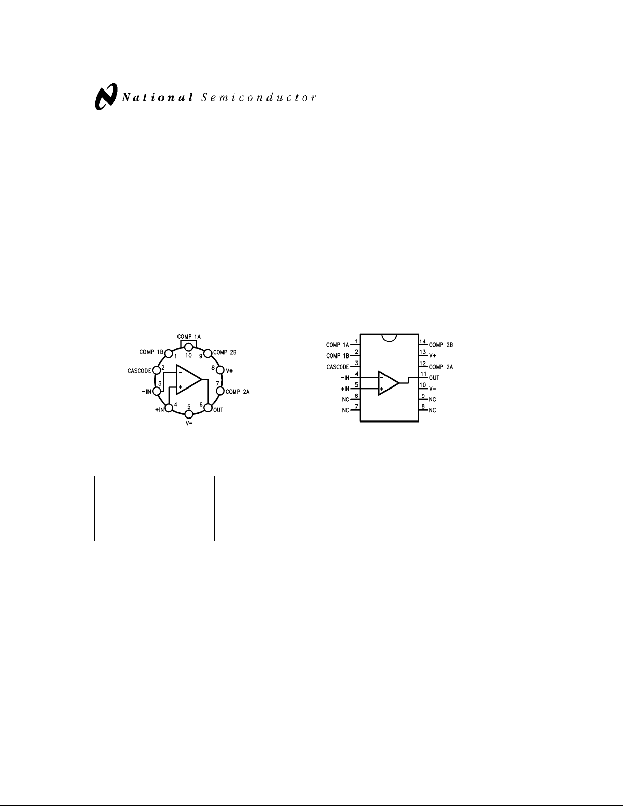
Connection Diagrams
10-Lead Metal Package
TL/H/10059– 1
Top View
Lead 5 connected to case.
Ordering Information
Device Package Package
Code Code Description
LM715MH H10C Metal
LM715CH H10C Metal
LM715MJ J14A Ceramic DIP
LM715CJ J14A Ceramic DIP
Features
Y
High slew rateÐ 100 V/ms
(Inverting, A
Y
Fast settling timeÐ 800 ns typically
Y
Wide bandwidthÐ 65 MHz typically
Y
Wide operating supply range
Y
Wide input voltage ranges
e
V
1) typically
Applications
Y
Video amplifiers
Y
Active filters
Y
High speed data conversion
14-Lead DIP
Top View
TL/H/10059– 2
C
1995 National Semiconductor Corporation RRD-B30M115/Printed in U. S. A.
TL/H/10059
Page 2
Absolute Maximum Ratings
If Military/Aerospace specified devices are required,
please contact the National Semiconductor Sales
Office/Distributors for availability and specifications.
Storage Temperature Range
Operating Temperature Range
Extended (LM715M)
Commercial (LM715C) 0
b
65§Ctoa175§C
b
55§Ctoa125§C
Ctoa70§C
§
Lead Temperature
Metal Can and Ceramic DIP
(Soldering, 60 sec.) 300
C
§
LM715M and LM715C
Electrical Characteristics
Symbol Parameter Conditions
V
IO
I
IO
I
IB
Z
I
R
O
I
CC
P
c
V
IR
A
VS
V Settling Time V
TR Transient Rise Time V
SR Slew Rate A
The following specifications apply over the range ofb55§CsT
LM715C
Symbol Parameter Conditions
V
IO
I
IO
I
IB
CMR Common Mode R
PSRR Power Supply R
A
VS
V
OP
Note 1: T
Note 2: Ratings apply to ambient temperature at 25
Note 3: For supply voltages less than
Note 4: T
Input Offset Voltage R
Input Offset Current 70 250 70 250 nA
Input Bias Current 400 750 400 1500 nA
Input Impedance 1.0 1.0 MX
Output Resistance 75 75 X
Supply Current 5.5 7.0 5.5 10 mA
Power Consumption 165 210 165 300 mW
Input Voltage Range
Large Signal Voltage Gain R
Response
Overshoot 25 40 25 50 %
Input Offset Voltage R
Input Offset Current T
Input Bias Current T
Rejection (Note 4) (Note 4)
Rejection Ratio (Note 4) (Note 4)
Large Signal R
Voltage Gain V
Output Voltage Swing R
e
175§C.
J Max
g
e
A
25§C only.
15V, the absolute maximum input voltage is equal to the supply voltage.
e
T
25§C, V
A
s
S
t
L
O
e
I
e
V
e
A
V
e
A
V
e
A
V
CC
10 kX 2.0 5.0 2.0 7.5 mV
2.0 kX,V
g
5.0V, A
400 mV, A
O
V
V
e
100 70 70
10 38 38
1.0 (Non-Inverting) 15 18 10 18
1.0 (Inverting) 100 100
Min Typ Max Min Typ Max
s
10 kX 7.5 10 mV
S
e
T
A
A Max
e
T
T
A
A Min
e
T
A
A Max
e
T
T
A
A Min
s
10 kX
S
s
10 kX
S
t
2.0 kX,
L
e
g
10V
O
e
2.0 kX
L
C. Above this temperature, derate the 10L-Metal Can at 7.1 mW/§C, and the 14L-Ceramic DIP at 9.1 mW/§C.
§
74 92
10 8 V/mV
g
Internal Power Dissipation (Notes 1, 2)
10L-Metal Can 1.07W
14L-Ceramic DIP 1.36W
Supply Voltage
Differential Input Voltage
Input Voltage (Note 3)
e
g
15V, unless otherwise specified
LM715M LM715C
Min Typ Max Min Typ Max
g10g
e
g
10V 15 30 10 30 V/mV
e
1.0 800 800 ns
e
1.0 30 60 30 75 ns
s
a
125§C for the LM715M, and 0§CsT
A
12
g10g
12 V
s
a
70§C for the
A
LM715M LM715C
250 250
800 750
0.75 1.5
4.0 7.5
74 92
45 400
g
13 V
10
45 300
g
13
g
10
g
g
g
Units
V/ms
Units
mV/V
18V
5V
15V
nA
mA
dB
2
Page 3
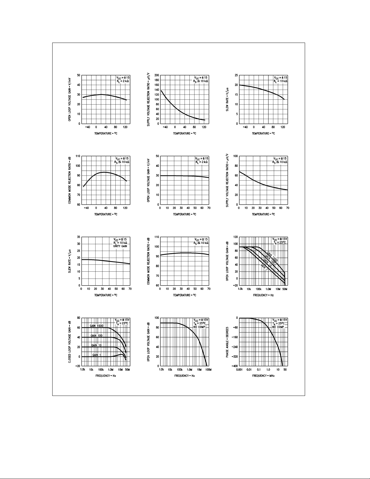
Typical Performance Characteristics for LM715M and LM715C
Voltage Gain vs
Temperature (LM715)
Common Mode Rejection Ratio
vs Temperature (LM715)
Slew Rate vs
Temperature (LM715C)
Supply Voltage Rejection Ratio
vs Temperature (LM715)
Voltage Gain vs
Temperature (LM715C)
Common Mode Rejection Ratio
vs Temperature (LM715C)
Slew Rate vs
Temperature (LM715)
Supply Voltage Rejection Ratio
vs Temperature (LM715C)
Frequency Response for Open
Loop Gains (Note 1)
Frequency Response for
Closed Loop Gains
Note 1: See ‘‘Non-Inverting Compensation Components Value Table’’ for Closed Loop Gain values.
Voltage Gain vs Frequency vs Frequency
3
Open Loop Phase
TL/H/10059– 4
Page 4

Typical Performance Characteristics for LM715M and LM715C (Continued)
Output Swing vs Frequency
for Closed Loop Gains
Unity Gain Large Signal
Pulse Response
Slew Rate vs Closed
Loop Voltage Gain
Supply Voltage Rejection
Ratio vs Frequency
Large Signal Pulse
Response for Gain 10
Slew Rate vs
Supply Voltage
Common Mode Rejection
Ratio vs Frequency
Large Signal Pulse
Response for Gain 100
Voltage Follower
Transient Response
Inverting Unity Gain Large
Signal Pulse Response
Small Signal Pulse Response
Inverting Unity Gain
TL/H/10059– 5
4
Page 5

Typical Performance Characteristics for LM715M and LM715C (Continued)
Voltage Follower (Note 2)
TL/H/10059– 6
Note 2: Lead numbers apply to metal package.
Equivalent Circuit
Voltage Offset Null Circuit (Note 2)
TL/H/10059– 7
High Slew Rate Circuit (Note 2)
TL/H/10059– 8
TL/H/10059– 3
5
Page 6

Applications Information
Non-Inverting Compensation
Components Values
Closed Loop
Gain
1000 10 pF
100 50 pF 250 pF
10 (Note) 100 pF 500 pF 1000 pF
1 500 pF 2000 pF 1000 pF
Note: For gain 10, compensation may be simplified by removing C2, C3 and
adding a 200 pF capacitor (C4) between Lead 7 and 10.
Frequency Compensation Circuit
C1 C2 C3
TL/H/10059– 9
RingingÐExcessive ringing (long acquisition time) may occur with large capacitive loads. This may be reduced by
isolating the capacitive load with a resistance of 100X.
Large source resistances may also give rise to the same
problem and this may be decreased by the addition of a
capacitance across the feedback resistance. A value of
around 50 pF for unity gain configuration and around 3.0 pF
for gain 10 should be adequate.
Latch UpÐThis may occur when the amplifier is used as a
voltage follower. The inclusion of a diode between leads 6
and 2 with the cathode toward lead 2 is the recommended
preventive measure.
Typical Applications
Suggested Values of Compensation Capacitors vs
Closed Loop Voltage Gain
TL/H/10059– 10
Layout Instructions
LayoutÐThe layout should be such that stray capacitance
is minimal.
SuppliesÐThe supplies should be adequately bypassed.
Used of 0.1 mF high quality ceramic capacitors is recommended.
TL/H/10059– 14
High Speed Integrator
TL/H/10059– 13
Note: All lead numbers on this page apply to metal package.
6
Page 7

Typical Applications (Continued)
Wide Band Video Amplifier Drive
Capability with 75X Coax Cable
TL/H/10059– 11
Note: All lead numbers shown refer to metal package.
Physical Dimensions inches (millimeters)
TL/H/10059– 12
10-Lead Metal Can Package (H)
Order Number LM715CH or LM715MH
NS Package Number H10C
7
Page 8

Physical Dimensions inches (millimeters) (Continued)
LM715 High Speed Operational Amplifier
14-Lead Ceramic Dual-In-Line Package (J)
Order Number LM715CJ or LM715MJ
NS Package Number J14A
LIFE SUPPORT POLICY
NATIONAL’S PRODUCTS ARE NOT AUTHORIZED FOR USE AS CRITICAL COMPONENTS IN LIFE SUPPORT
DEVICES OR SYSTEMS WITHOUT THE EXPRESS WRITTEN APPROVAL OF THE PRESIDENT OF NATIONAL
SEMICONDUCTOR CORPORATION. As used herein:
1. Life support devices or systems are devices or 2. A critical component is any component of a life
systems which, (a) are intended for surgical implant support device or system whose failure to perform can
into the body, or (b) support or sustain life, and whose be reasonably expected to cause the failure of the life
failure to perform, when properly used in accordance support device or system, or to affect its safety or
with instructions for use provided in the labeling, can effectiveness.
be reasonably expected to result in a significant injury
to the user.
National Semiconductor National Semiconductor National Semiconductor National Semiconductor
Corporation Europe Hong Kong Ltd. Japan Ltd.
1111 West Bardin Road Fax: (
Arlington, TX 76017 Email: cnjwge@tevm2.nsc.com Ocean Centre, 5 Canton Rd. Fax: 81-043-299-2408
Tel: 1(800) 272-9959 Deutsch Tel: (
Fax: 1(800) 737-7018 English Tel: (
National does not assume any responsibility for use of any circuitry described, no circuit patent licenses are implied and National reserves the right at any time without notice to change said circuitry and specifications.
Fran3ais Tel: (
Italiano Tel: (
a
49) 0-180-530 85 86 13th Floor, Straight Block, Tel: 81-043-299-2309
a
49) 0-180-530 85 85 Tsimshatsui, Kowloon
a
49) 0-180-532 78 32 Hong Kong
a
49) 0-180-532 93 58 Tel: (852) 2737-1600
a
49) 0-180-534 16 80 Fax: (852) 2736-9960
 Loading...