

NSC LM6365N, LM6365MX, LM6365M Datasheet
LM6165/LM6265/LM6365
High Speed Operational Amplifier
General Description
The LM6165 family of high-speed amplifiers exhibits an excellent speed-power product in delivering 300 V/µs and
725 MHz GBW (stable for gains as low as +25) with only
5 mA of supply current. Further power savings and application convenience are possible by taking advantage of the
wide dynamic range in operating supply voltage which extends all the way down to +5V.
These amplifiers are built with National’s VIP
™
(VerticallyIntegrated PNP) process which produces fast PNP transistors
that are true complements to the already fast NPN devices.
This advanced junction-isolated process delivers high speed
performance without the need for complex and expensive dielectric isolation.
Features
n High slew rate: 300 V/µs
n High GBW product: 725 MHz
n Low supply current: 5 mA
n Fast settling: 80 ns to 0.1
%
n Low differential gain:
<
0.1
%
n Low differential phase:
<
0.1˚
n Wide supply range: 4.75V to 32V
n Stable with unlimited capacitive load
Applications
n Video amplifier
n Wide-bandwidth signal conditioning
n Radar
n Sonar
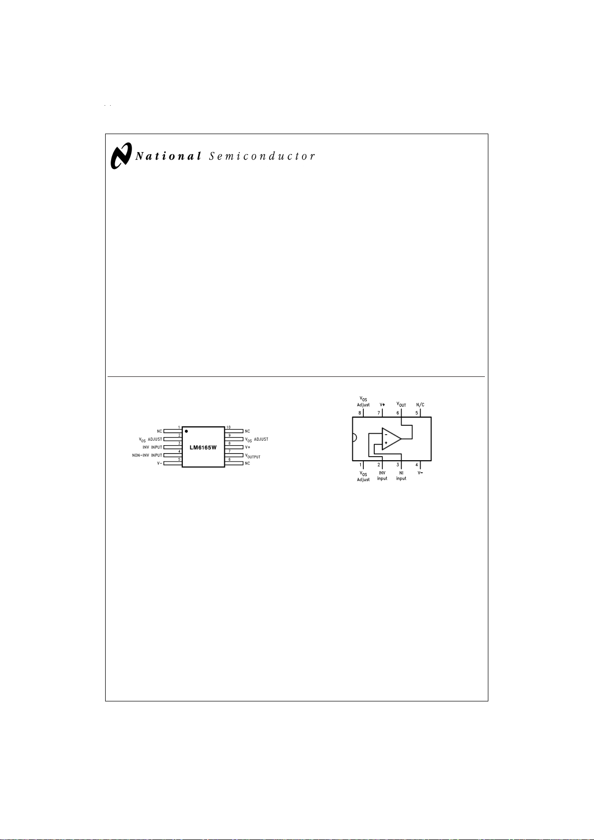
Connection Diagrams
VIP™is a trademark of National SemiconductorCorporation.
10-Lead Flatpak
Top View
DS009152-14
Order Number LM6165W/883
See NS Package Number W10A
DS009152-8
Order Number LM6165J/883
See NS Package Number J08A
Order Number LM6365M
See NS Package Number M08A
Order Number LM6265N or LM6365N
See NS Package Number N08E
May 1999
LM6165/LM6265/LM6365 High Speed Operational Amplifier
© 1999 National Semiconductor Corporation DS009152 www.national.com
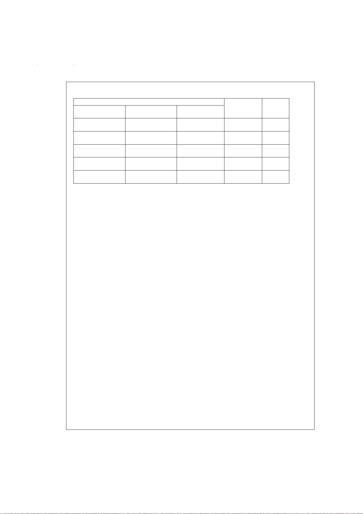
Connection Diagrams (Continued)
Temperature Range Package NSC
Drawing
Military Industrial Commercial
−55˚C ≤ T
A
≤ +125˚C −25˚C ≤ TA≤ +85˚C 0˚C ≤ TA≤ +70˚C
LM6265N LM6365N 8-Pin N08E
Molded DIP
LM6165J/883 8-Pin J08A
5962-8962501PA Ceramic DIP
LM6365M 8-Pin Molded M08A
Surface Mt.
LM6165WG/883 10-Lead WG10A
5962-8962501XA Ceramic SOIC
LM6165W883 10-Pin W10A
5962-8962501HA Ceramic Flatpak
www.national.com 2
Absolute Maximum Ratings (Note 1)
If Military/Aerospace specified devices are required,
please contact the National Semiconductor Sales Office/
Distributors for availability and specifications.
Supply Voltage (V
+−V−
) 36V
Differential Input Voltage
(Note 7)
±
8V
Common-Mode Voltage
Range (Note 11) (V
+
− 0.7V) to (V−+ 0.7V)
Output Short Circuit to GND
(Note 2) Continuous
Soldering Information
Dual-In-Line Package (N, J)
Soldering (10 sec.) 260˚C
Small Outline Package (M)
Vapor Phase (60 sec.)
Infrared (15 sec.)
215˚C
220˚C
See AN-450 “Surface Mounting Methods and Their Effect
on Product Reliability” for other methods of soldering
surface mount devices.
Storage Temp Range −65˚C to +150˚C
Max Junction Temperature
(Note 3) 150˚C
ESD Tolerance (Notes 7, 8)
±
700V
Operating Ratings
Temperature Range (Note 3)
LM6165, LM6165J/883 −55˚C ≤ T
J
≤ +125˚C
LM6265 −25˚C ≤ T
J
≤ +85˚C
LM6365 0˚C ≤ T
J
≤ +70˚C
Supply Voltage Range 4.75V to 32V
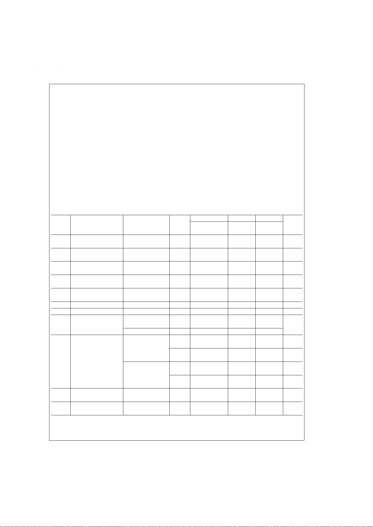
DC Electrical Characteristics
The following specifications apply for Supply Voltage
=
±
15V, V
CM
=
0, R
L
≥ 100 kΩ and R
S
=
50Ω unless otherwise noted.
Boldface limits apply for T
A
=
T
J
=
T
MIN
to T
MAX
; all other limits T
A
=
T
J
=
25˚C.
Symbol Parameter Conditions Typ LM6165 LM6265 LM6365 Units
Limit Limit Limit
(Notes 4, 12) (Note 4) (Note 4)
V
OS
Input Offset Voltage 1 3 3 6 mV
447Max
V
OS
Input Offset Voltage 3 µV/˚C
Drift Average Drift
I
b
Input Bias Current 2.5 3 3 5 µA
656Max
I
OS
Input Offset Current 150 350 350 1500 nA
800 600 1900 Max
I
OS
Input Offset Current 0.3 nA/˚C
Drift Average Drift
R
IN
Input Resistance Differential 20 kΩ
C
IN
Input Capacitance 6.0 pF
A
VOL
Large Signal V
OUT
=
±
10V, 10.5 7.5 7.5 5.5 V/mV
Min
Voltage Gain R
L
=
2kΩ 5.0 6.0 5.0
(Note 10) R
L
=
10 kΩ 38
V
CM
Input Common-Mode Supply
=
±
15V +14.0 +13.9 +13.9 +13.8 V
Voltage Range +13.8 +13.8 +13.7 Min
−13.6 −13.4 −13.4 −13.3 V
−13.2 −13.2 −13.2 Min
Supply=+5V 4.0 3.9 3.9 3.8 V
(Note 5) 3.8 3.8 3.7 Min
1.4 1.6 1.6 1.7 V
1.8 1.8 1.8 Max
CMRR Common-Mode −10V ≤ V
CM
≤ +10V 102 88 88 80 dB
Rejection Ratio 82 84 78 Min
PSRR Power Supply
±
10V ≤ V±≤±16V 104 88 88 80 dB
Rejection Ratio 82 84 78 Min
www.national.com3
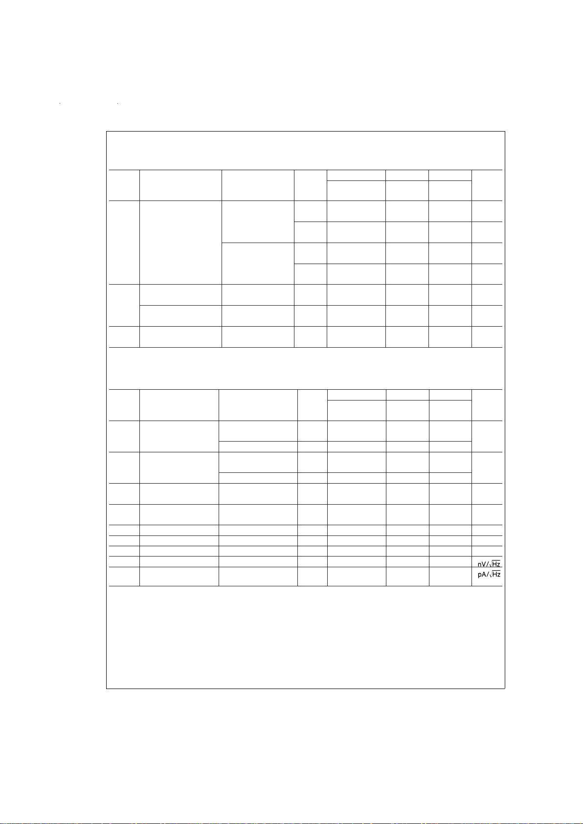
DC Electrical Characteristics (Continued)
The following specifications apply for Supply Voltage
=
±
15V, V
CM
=
0, R
L
≥ 100 kΩ and R
S
=
50Ω unless otherwise noted.
Boldface limits apply for T
A
=
T
J
=
T
MIN
to T
MAX
; all other limits T
A
=
T
J
=
25˚C.
Symbol Parameter Conditions Typ LM6165 LM6265 LM6365 Units
Limit Limit Limit
(Notes 4, 12) (Note 4) (Note 4)
V
O
Output Voltage Supply
=
±
15V, +14.2 +13.5 +13.5 +13.4 V
Swing R
L
=
2kΩ +13.3 +13.3 +13.3 Min
−13.4 −13.0 −13.0 −12.9 V
−12.7 −12.8 −12.8 Min
Supply=+5V 4.2 3.5 3.5 3.4 V
R
L
=
2kΩ(Note 5) 3.3 3.3 3.3 Min
1.3 1.7 1.7 1.8 V
2.0 1.9 1.9 Max
Output Short Source 65 30 30 30 mA
Circuit Current 20 25 25 Min
Sink 65 30 30 30 mA
20 25 25 Min
I
S
Supply Current 5.0 6.5 6.5 6.8 mA
6.8 6.7 6.9 Max
AC Electrical Characteristics
The following specifications apply for Supply Voltage
=
±
15V, V
CM
=
0, R
L
≥ 100 kΩ and R
S
=
50Ω unless otherwise noted.
Boldface limits apply for T
A
=
T
J
=
T
MIN
to T
MAX
; all other limits T
A
=
T
J
=
25˚C. (Note 6)
Symbol Parameter Conditions Typ LM6165 LM6265 LM6365 Units
Limit Limit Limit
(Notes 4, 12) (Note 4) (Note 4)
GBW Gain Bandwidth F=20 MHz 725 575 575 500 MHz
Min
350
Product Supply
=
±
5V 500
SR Slew Rate A
V
=
+25 (Note 9) 300 200 200 200 V/µs
Min
180
Supply
=
±
5V 200
PBW Power Bandwidth V
OUT
=
20 V
PP
4.5 MHz
Product
t
S
Settling Time 10V Step to 0.1
%
80 ns
A
V
=
−25, R
L
=
2kΩ
φ
m
Phase Margin A
V
=
+25 45 Deg
A
D
Differential Gain NTSC, A
V
=
+25
<
0.1
%
φ
D
Differential Phase NTSC, A
V
=
+25
<
0.1 Deg
e
np-p
Input Noise Voltage F=10 kHz 5
i
np-p
Input Noise Current F=10 kHz 1.5
Note 1: “Absolute Maximum Ratings” indicate limits beyond which damage to the device may occur. Operating Ratings indicate conditions for which the device is
functional, but do not guarantee specific performance limits.
Note 2: Continuous short-circuit operation at elevated ambient temperature can result in exceeding the maximum allowed junction temperature of 150˚C.
Note 3: The typical junction-to-ambient thermal resistance of the molded plastic DIP (N) is 105˚C/Watt, and the molded plastic SO (M) package is 155˚C/Watt, and
the cerdip (J) package is 125˚C/Watt. All numbers apply for packages soldered directly into a printed circuit board.
Note 4: All limits guaranteed by testing or correlation.
Note 5: For single supply operation, the following conditions apply: V+=5V, V−=0V, V
CM
=
2.5C, V
OUT
=
2.5V. Pin1&Pin8(V
OS
Adjust) are each connected
to Pin 4 (V−) to realize maximum output swing. This connection will degrade V
OS
.
Note 6: C
L
≤ 5pF.
Note 7: In order to achieve optimum AC performance, the input stage was designed without protective clamps. Exeeding the maximum differential input voltage results in reverse breakdown of the base-emitter junction of one of the input transistors and probable degradation of the input parameters (especially V
OS,IOS
, and
Noise).
www.national.com 4
 Loading...